Abstrak
Pada saat ini teknologi robot berkembang dengan sangat cepat. Robot-robot tersebut banyak digunakan dalam berbagai bidang seperti: bidang penelitian, industri, kedokteran, eksplorasi ruang angkasa dan lain-lain. Salah satu jenis robot yang banyak digunakan dalam bidang industri yaitu robot yang dapat mengikuti lintasan garis tertentu (line follower robot). Pada umumnya robot tipe ini berbentuk kendaraan.
Realisasi hardware dari line follower robot menggunakan penjejakan sensor inframerah untuk mendeteksi garis lintasan berwarna hitam pada bidang alas berwarna putih. Sensor yang digunakan berupa sensor optocoupler sebanyak enam buah. Pengaturan kecepatan dari motor dc dilakukan dengan metoda PWM oleh mikrokontroler. Mikrokontroler ATMega16 ini juga sebagai pengatur kerja antara satu komponen dengan yang lain. Metoda pengendalian yang digunakan adalah logika fuzzy, namun proses perhitungan logika fuzzy dilakukan di luar mikrokontroler, dengan menggunakan software petrafuz. Hasil input dan output logika fuzzy tersebut kemudian disimpan ke dalam mikrokontroler. Lintasan yang diuji coba berupa garis lintasan lurus, belok melengkung dan persimpangan.
Hasil percobaan yang dilakukan menunjukkan bahwa kendaraan dapat mengikuti bentuk garis lintasan yang harus diikuti. Jadi dapat disimpulkan, realisasi kendaraan secara hardware berhasil dibuat. Sedangkan untuk pengendali dengan logika fuzzy, hasil yang dicapai masih belum sempurna. Hal ini karena penulis mengalami kesulitan dalam membuat program pengendali logika fuzzy. Sehingga pengendali logika fuzzy yang dipakai belum dapat dilakukan oleh mikrokontroler sendiri.
Universitas Kristen Maranatha
Abstract
In the past few years, the development of robotic technology is growing very rapidly. Those robots are use in many different fields, such as: experimental, medical, industrial, space exploration and etc. One type of robot that commonly use in industrial fields is a line follower robot.
This final project goal is to make a realization of a line follower robot using fuzzy logic controller. This robot is using six infrared sensors (optocoupler sensor) to detect a black line in a white background. The dc motor speed is controlled by microcontroller’s PWM output. This microcontroller also works as a control center for other components. The controller of this line follower robot is using a fuzzy logic control. However the computation of fuzzy logic Is done by using Petrafuz software. Then the input and output value from Petrafuz software will be store in microcontroller. The shapes of tracks that will be test are a straight line, a slope curve with 900 angle and a cross section.
The experiment showed that the line follower robot is capable in following the shapes of tracks. From the result, we can say that the realization of a line follower robot is succeed. However for the fuzzy logic controller is not perfect. This because the computation process of fuzzy logic is not done by microcontroller itself.
Universitas Kristen Maranatha
KATA PENGANTAR
Pertama-tama, puji dan syukur kepada Tuhan Yang Maha Esa karena atas berkat dan rahmat-Nya, penulis dapat menyelesaikan laporan tugas akhir ini tepat pada waktunya.
Tugas Akhir yang berjudul “Realisasi Kendaraan Yang Mengikuti
Suatu Lintasan Tertentu Dengan Pengendali Logika Fuzzy“ dibuat untuk
memenuhi persyaratan program studi Strata Satu Fakultas Teknik Jurusan Teknik Elektro di Universitas Kristen Maranatha.
Dalam menyelesaikan tugas akhir ini bukan suatu hal yang mudah, banyak halangan dan masalah yang yang harus dihadapi karena keterbatasan pengalaman dan pengetahuan. Penulis menyadari bahwa tanpa anugerah Tuhan, serta bantuan dari berbagai pihak, tidak dapat menyelesaikan tugas akhir ini dengan baik. Oleh karena itu, tidak lupa penulis ucapkan banyak terima kasih kepada pihak-pihak yang telah membantu dalam pengerjaan kerja praktek ini, yaitu:
1. Bapak Agustinus, ST.,MT. selaku pembimbing pertama tugas akhir yang telah memberikan masukan pengetahuan dan ide-ide serta membimbing dalam pembuatan tugas akhir ini.
2. Bapak Muliady, ST., MT. selaku pembimbing kedua tugas akhir yang telah mendorong dan memberikan masukan serta pemecahan masalah dalam menyelesaikan tugas akhir ini.
3. Bapak Ir. Aan Darmawan, MT., selaku Ketua Jurusan Teknik Elektro perioda 2004-2008 yang telah membantu memberikan kesempatan dan masukan-masukan dalam menyelesaikan tugas akhir ini..
4. Ibu Ir. Anita Supartono Msc., selaku koordinator TA yang tetap mendorong serta memberikan kesempatan untuk menyelesaikan tugas akhir ini.
5. Kepada bapak dan ibu yang bekerja di bagian Tata Usaha Jurusan Teknik Elektro.
Universitas Kristen Maranatha
6. Kepada bapak Ade dan bapak Endang yang bekerja di Laboratorium Elektronika dan Laboratorium Fisika yang telah membantu menyediakan peralatan-peralatan yang dibutuhkan.
7. Kepada bapak dan ibu yang bekerja di bagian Perpustakaan Fakultas Teknik.
8. Papa, mama, atas dorongan moril dan dukungan doa yang telah menguatkan penulis.
9. Tony, Heru, Yence, Alex, Andris, Harrison, Tina, Pohan, Citra, Mario Koba, Willy, Nico, dan Dennis yang telah memberikan dukungan moril dan bantuan dalam mengerjakan tugas akhir ini.
10.Teman-teman dan pihak-pihak lain yang telah membantu dalam mengerjakan tugas akhir ini, yang tidak dapat disebutkan satu-persatu. Demikian tugas akhir ini disusun, sehingga kiranya dapat memberikan pemahaman dan tambahan pengetahuan bagi pembaca pada umumnya dan mahasiswa secara khusus. Penulis juga menyadari bahwa laporan ini jauh dari sempurna sehingga apabila ditemukan kesalahan, penulis mohon maaf yang sebesar-besarnya. Penulis juga mengharapkan kritik dan saran dari pembaca.
Bandung, Juli 2006
Penulis
Universitas Kristen Maranatha
DAFTAR ISI
Halaman
LEMBAR PENGESAHAN SURAT PERNYATAAN
ABSTRAK ... i
ABSTRACT...ii
KATA PENGANTAR ... iii
DAFTAR ISI ... v
DAFTAR GAMBAR ... viii
DAFTAR TABEL ...xi
DAFTAR RUMUS ... xii
BAB I PENDAHULUAN ... 1
I.1. Latar Belakang ... 1
I.2. Identifikasi masalah ... 2
I.3. Tujuan ... 2
I.4. Spesifikasi Alat ... 2
I.5. Pembatasan Masalah... 2
I.6. Sistematika Penulisan ... 3
BAB II LANDASAN TEORI ... 5
II.1. Definisi Robot ... 5
II.1.1. Klasifikasi Robot... 6
II.1.1.1. Klasifikasi Robot berdasarkan Sistem Koordinat .... 7
II.1.1.2. Klasifikasi Robot berdasarkan Metoda kendali ... 11
II.2. Sensor ... 12
II.2.1. Infra Merah ... 13
II.3. Logika Fuzzy ... 15
II.3.1 Himpunan Fuzzy ... 16
II.3.1.1. Fungsi Keanggotaan Himpunan Fuzzy ... 19
II.3.1.2. Aturan Fuzzy Jika-Maka... 22
II.3.2 Fuzzy Interface Systems (FIS) ... 22
II.3.2.1. Fuzzifikasi ... 23
Universitas Kristen Maranatha
II.3.2.2. Operator Fuzzy ... 24
II.3.2.3. Metoda Implikasi ... 25
II.3.2.4. Agresi Keluaran ... 25
II.3.2.5. Defuzzifikasi... 26
II.3.2.6. Metoda Fuzzy Tipe Sugeno ... 27
II.4. Mikrokontroler... 28
II.4.1 Memori ... 28
II.4.2 Bagian Input/Output (I/O) ... 29
II.4.3 Peripheral Mikrokontroler ATmega16 ... 30
II.4.4 Sleep Mode ... 36
II.4.5 Mode Pengalamatan ... 37
II.4.6 Perangkat Lunak ... 41
II.4.6.1. AVR Studio 4 ... 43
II.4.6.2. Perangkat Antarmuka antara Komputer dengan Mikrokontroler ... 44
II.4.6.2.1. Perangkat Keras Antara Komputer dengan Mikrokontroler ... 45
II.4.6.2.2. Perangkat Lunak Antara Komputer dengan Mikrokontroler ... 45
II.4.6.3. Petrafuz ... 46
BAB III PERANCANGAN PERANGKAT KERAS DAN LUNAK ... 48
III.1. Diagram Blok... 48
III.2. Perancangan Perangkat Keras ... 51
III.3.1. Rangkaian Catu Daya ... 51
III.3.2. Sensor Lintasan Garis ... 52
III.3.3. Rangkaian Output Motor DC ... 54
III.3.4. Mikrokontroller ATmega16 ... 55
III.3. Perancangan Perangkat Lunak ... 56
III.3.1. Perancangan Logika Fuzzy ... 57
III.3.1.1. Fungsi Keanggotaan Input Himpunan Fuzzy ... 59
III.3.1.2. Fungsi Keanggotaan Output Himpunan Fuzzy ... 60
III.3.2. Perancangan Program Mikrokontroller ... 61
Universitas Kristen Maranatha
BAB IV Data Pengamatan Kendaraan Yang Mengikuti Suatu Lintasan Tertentu ... 70 IV.1. Posisi Sensor dengan Bidang Lintasan ... 70 IV.2. Hasil Input-Output Pengendali Logika Fuzzy dengan
Software Petrafuz... 72 IV.3. Pengamatan Jalan Kendaraan Yang Mengikuti Garis
Lintasan Tertentu ... 74 BAB V KESIMPULAN DAN SARAN ... 77 DAFTAR PUSTAKA... 78 LAMPIRAN A Gambar Foto Alat ... A LAMPIRAN B Skema Rangkaian Alat... B LAMPIRAN C Perangkat Lunak ...C LAMPIRAN D Datasheet Komponen ...D
Universitas Kristen Maranatha
DAFTAR GAMBAR
Halaman
Gambar 2.1 Robot Cantilevered Cartesian ... 7
Gambar 2.2 Robot Gantry-Style Cartesian... 8
Gambar 2.3 Robot Koordinat Cylindrical... 8
Gambar 2.4 Robot Koordinat Spherical... 9
Gambar 2.5 Robot Joint Spherical Murni ... 9
Gambar 2.6 Robot Parallelogram Spherical... 10
Gambar 2.7 Robot Cylindrical Joint... 10
Gambar 2.8 Diagram Blok Sensor Optocoupler... 12
Gambar 2.9 Sensor Optocoupler... 12
Gambar2.10 Daerah Frekuensi Gelombang Infra Merah ... 13
Gambar2.11 Daerah Panjang Gelombang Infra Merah... 14
Gambar2.12 Himpunan Fuzzy dan Fungsi Keangggotaannya... 17
Gambar2.13 Diagram Venn Gabungan Dua Himpunan ... 17
Gambar2.14 Diagram Venn Irisan dua Himpunan ... 18
Gambar2.15 Diagram Venn Komplemen Dua Himpunan... 18
Gambar 2.16a Fungsi Keanggotaan Himpunan Logika Konvensional... 19
Gambar 2.16b Fungsi Keanggotaan Himpunan Logika Fuzzy... 19
Gambar 2.17 Fungsi Keanggotaan S ... 20
Gambar 2.18 Fungsi Keanggotaan π... 20
Gambar 2.19 Fungsi Keanggotaan Trapesium ... 21
Gambar 2.20 Fungsi Keanggotaan Segitiga ... 21
Gambar 2.21 Fungsi Keanggotaan Gauss... 22
Gambar 2.22 Arsitektur Fuzzy Interface System ... 23
Gambar 2.23 Proses Fuzzifikasi ... 23
Gambar 2.24 Proses Aplikasi Operator OR Metoda MAX ... 24
Gambar 2.25 Proses Impilkasi Metoda MIN ... 25
Gambar 2.26 Proses Agresi Keluaran dengan Metoda MAX... 26
Gambar 2.27 Arsitektur Atmega16 ... 31
Universitas Kristen Maranatha
Gambar 2.28 Blok Diagram ATmega16 ... 32
Gambar 2.29 Mikrokontroller Atmega16 ... 33
Gambar 2.30 Instruksi Sleep Mode ... 36
Gambar 2.31 Direct Single Register Addressing... 38
Gambar 2.32 Direct Register Addressing dengan 2 register... 38
Gambar 2.33 I/O Direct Addressing... 39
Gambar 2.34 Data Indirect Addressing with Pre-Decrement... 39
Gambar 2.35 Data Indirect Addressing with Post-increment... 40
Gambar 2.36 Program Memory Constant Addressing... 40
Gambar 2.37 Program Memory with post-Increment... 41
Gambar 2.38 Tampilan Programmer AVR Studio 4 ... 44
Gambar 2.39 Diagram Blok AVR ISP ... 45
Gambar 2.40 Tampilan dari Software downloader ALL-11 ... 46
Gambar 2.41 Tampilan Software Petrafuz... 47
Gambar 3.1 Blok Diagram Robot... 48
Gambar 3.2 Blok Kerja Alat ... 49
Gambar 3.3 Rangkaian Catu Daya Mikrokontroler dan Sensor ... 51
Gambar 3.4 Rangkaian Catu Daya untuk Motor DC ... 52
Gambar 3.5 Rangkaian Sensor Optocoupler... 53
Gambar 3.6 Posisi Sensor GP2S28 pada badan PCB ... 53
Gambar 3.7 Skema Rangkaian Kendaraan ... 56
Gambar 3.8Flowchart Logika Fuzzy untuk Line Follower ... 58
Gambar 3.9 Bentuk Membership Function untuk Input Error dan Derror 59 Gambar 3.10 Bentuk membership Function Output... 60
Gambar 3.11 Flowchart Sistem ... 63
Gambar 3.12 Flowchart Subroutine PB ... 64
Gambar 3.13 Flowchart Subroutine PS ... 65
Gambar 3.14 Flowchart Subroutine NS ... 66
Gambar 3.15 Flowchart Subroutine NB ... 67
Gambar 3.16 Flowchart Subroutine Z ... 68
Gambar 3.17 Flowchart Subroutine Tunda ... 68
Gambar 3.18 Flowchart Subroutine Sleep ... 69
Universitas Kristen Maranatha
Gambar 4.1 Pantulan Sensor Terhadap Bidang Lintasan... 71
Universitas Kristen Maranatha
DAFTAR TABEL
Halaman
Tabel 2..1 Fungsi Pengganti Port B ... 34
Tabel 2.2 Fungsi Pengganti Port C ... 35
Tabel 2.3 Fungsi Pengganti Port D ... 35
Tabel 2.4 Nilai bit SM0, SM1, SM2 untuk menentukan mode sleep .... 37
Tabel 3.1 Membership Function Input dan posisi point-pointnya ... 60
Tabel 3.2 Membership Function Output dan posisi point-pointnya ... 61
Tabel 3.3 Hasil Selisih Gain PWM dengan Logika Fuzzy ... 62
Tabel 4.1 Tegangan Output Sensor ... 71
Tabel 4.2 Tegangan Output Hasil Deteksi pada Input Sensor ... 72
Tabel 4.3 Tabel Selisih Gain dengan Pengendali Logika Fuzzy ...73
Tabel 4.4 Beberapa Nilai Input dan Output Fuzzy Hasil Petrafuz ... 73
Tabel 4.5 Pengamatan Gerak Kendaraan ... 74
Universitas Kristen Maranatha
DAFTAR RUMUS
Halaman
Rumus 2.1 ... 13
Rumus 2.2 ... 14
Rumus 2.3 ... 15
Rumus 2.4 ... 16
Rumus 2.5 ... 17
Rumus 2.6 ... 17
Rumus 2.7 ... 18
Rumus 2.8 ... 18
Rumus 2.9 ... 24
Rumus 2.10 ... 24
Rumus 2.11 ... 24
Rumus 2.12 ... 24
Rumus 2.13 ... 25
Rumus 2.14 ... 25
Rumus 2.15 ... 26
Rumus 2.16 ... 26
Rumus 2.17 ... 27
Universitas Kristen Maranatha
LAMPIRAN A
Foto Alat
LAMPIRAN B
Skema Rangkaian Alat
LAMPIRAN C
Perangkat Lunak
• Rule-rule Fuzzy Logic Control untuk kendaraan yang mengikuti
suatu lintasan tertentu dengan software Petrafuz.
1. IF error IS NB AND derror IS NB THEN selisihgain IS PB 2. IF error IS NB AND derror IS NS THEN selisihgain IS PS 3. IF error IS NB AND derror IS Z THEN selisihgain IS PS 4. IF error IS NB AND derror IS PS THEN selisihgain IS PB 5. IF error IS NB AND derror IS PB THEN selisihgain IS PB 6. IF error IS NS AND derror IS NB THEN selisihgain IS PS 7. IF error IS NS AND derror IS NS THEN selisihgain IS PS 8. IF error IS NS AND derror IS Z THEN selisihgain IS PB 9. IF error IS NS AND derror IS PS THEN selisihgain IS PB 10.IF error IS NS AND derror IS PB THEN selisihgain IS PB
• Program Mikrokontroler Perintah macro pada file avr.inc ;---; ; Load/store word dari/ke memori ;
; ldsw Z,mem
; ldiw Z,imm
.macro ldiw
ldi @0L,low(@1)
ldi @0H,high(@1)
.endm
.macro ldsw
lds @0L,@1
lds @0H,@1+1
.endm
.macro lddw
ldd @0L,@1
ldd @0H,@1+1
.endm
.macro stsw
sts @0,@1L
sts @0+1,@1H
.endm
.macro stdw
std @0,@1L
std @0+1,@1H
.endm
.macro pushw
push @0H
push @0L
.macro popw
pop @0L
pop @0H
.endm
;---; ; Operasi Word dengan dua register ;
.macro addiw
subi @0L,low(-(@1))
sbci @0H,high(-(@1))
.endm
.macro subiw
subi @0L,low(@1)
sbci @0H,high(@1)
.endm
.macro addw
add @0L,@1L
adc @0H,@1H
.endm
.macro adcw
adc @0L,@1L
adc @0H,@1H
.endm
.macro subw
sub @0L,@1L
sbc @0H,@1H
.endm
.macro sbcw
sbc @0L,@1L
sbc @0H,@1H
.macro cpw
cp @0L,@1L
cpc @0H,@1H
.endm
.macro cpcw
cpc @0L,@1L
cpc @0H,@1H
.endm
.macro andw
and @0L,@1L
and @0H,@1H
.endm
.macro andiw
andi @0L,low(@1)
andi @0H,high(@1)
.endm
.macro orw
or @0L,@1L
or @0H,@1H
.endm
.macro oriw
ori @0L,low(@1)
ori @0H,high(@1)
.endm
.macro lslw
lsl @0L
rol @0H
.endm
.macro lsrw
lsr @0H
ror @0L
.macro asrw
asr @0H
ror @0L
.endm
.macro rolw
rol @0L
rol @0H
.endm
.macro rorw
ror @0H
ror @0L
.endm
.macro clrw
clr @0L
clr @0H
.endm
.macro comw
com @0L
com @0H
.endm
.macro movew
mov @0L, @1L
mov @0H, @1H
.endm
.macro tstw
cp @0L, _0
cpc @0H, _0
.endm
.macro outw
out @0H, @1H
out @0L, @1L
.macro inw
in @0L, @1L
in @0H, @1H
.endm
;---; ; Output port immediate via r16
; outi port,var .macro outi
ldi r16,@1
out @0,r16
.endm
;---; ; Add immediate to register
.macro addi
subi @0,-(@1)
Program Utama
;---;
; Program Line Follower Robot
; Internal Oscillator 8 Mhz, dengan low fuse bit untuk bit CKSEL 01000 dan SUT: 10 (start up time 65ms);
; Mode sleep yang digunakan power-down, dan ; ; Timer0 dan Timer2 dipakai dalam mode PWM ; ;---;
.include "m16def.inc" .include "avr.inc"
.equ RAMTOP = 0x60 .equ bit0 = 0b00000001 .equ bit1 = 0b00000010 .equ bit2 = 0b00000100 .equ bit3 = 0b00001000 .equ bit4 = 0b00010000
.equ bit5 = 0b00100000 .equ bit6 = 0b01000000 .equ bit7 = 0b10000000
.equ setpoint = 0b00110011 .equ batasns = 0b00000110 .equ batasnb = 0b00001001 .equ batasps = 0b00001100 .equ bataspb = 0b00010100 .equ batasz = 0x00
.equ gainpb = 128 .equ gainps = 64 .equ gainz = 0 .equ gainns = 64 .equ gainnb = 128
.equ batasdens = 0b00000110 .equ batasdenb = 0b00001001 .equ batasdeps = 0b00001100 .equ batasdepb = 0b00010100 .equ batasdez = 0x00
;---;
; Tabel Interupsi ;
;---; .cseg
; jmp 0 ; interupt USART_RXC ; jmp 0 ; interupt USART_UDRE ; jmp 0 ; interupt USART_TXC ; jmp 0 ; interupt ADC
; jmp 0 ; interupt EE_RDY ; jmp 0 ; interupt ANA_COMP ; jmp 0 ; interupt TWI
; jmp 0 ; interupt INT2 ; jmp 0 ; interupt TIMER2_COMP ; jmp 0 ; interupt SPM_RDY ;---;
;---; ; POWER ON RESET/ POWER ON ; ;---;
RESET :
ldiw A, RAMEND ; inisialisasi Stack Pointer outw SP, A ;
clr err
outi DDRA, 0b00000000 ; inisialisasi PORTA outi PORTA, 0b00000000 ; /
outi DDRB, 0b01101011 ; Inisialisasi PORTB outi PORTB, 0b10010100 ; /
outi DDRC, 0b11111111 ; Inisialisasi PORTC outi PORTC, 0b00000000 ; /
outi DDRD, 0b11111111 ; Inisialisasi PORTD outi PORTD, 0b01111111 ; /
outi TCCR0, 0b01100101 ; Inisialisasi TIMER 0 untuk motor kiri
outi TCCR2, 0b01100111 ; Inisialisasi Timer 2 untuk motor kanan
outi OCR0, 0x7F
outi OCR2, 0x7F clr positif
clr speed
outi PORTB, 0b0100010 ; start motor kiri dan kanan
call delay
sei
;---;
; Program Utama ;
;---;
start:
rcall ceksensor cpi AL, 0x3F
breq cekerr
ldi simpan3, setpoint mov simpan1, AL cp simpan3, simpan1
brsh pos
brlo negatif
ceksensor:
outi PORTD, 0b01101010 ; pemancar sensor 1,3 dan 5 aktif
sbi PORTA, 6 ; penerima aktif
rcall wait
in AL, PORTA ; baca hasil di portA
outi PORTA, 0b01010101 ; pemancar sensor 2,4 dan 6 aktif
sbi PORTA, 6 ; penerima aktif
rcall wait
in AL, PORTA
or AL, AH
ret cekerr:
inc err
cpi err, 0x04
breq enter_SLEEP
rcall ceksensor cpi AL, 0x3F
breq cekerr
ret
enter_SLEEP : outi PORTA, 0b00000000
outi PORTB, 0b00100010 outi PORTC, 0b00000000 outi PORTD, 0b01111111 in r16, SREG
clr positif
outi MCUCR, 0b10110011 sleep
ret
terus:
mov Esblm, E
rcall delay
pos:
sbr positif, 0 sub simpan3, simpan1 mov E, simpan3
cpi E, bataspb
brsh epb
brlo cekeps
epb:
rcall pb
rjmp terus
cekeps:
cpi E, batasps
brsh eps
brlo ez
eps:
rcall ps
rjmp terus
negatif:
cbr positif, 0 mov simpan2, simpan1 sub simpan2, simpan3 mov E, simpan2
cpi E, batasnb
brsh enb
brlo cekens
enb:
rcall nb
rjmp terus
cekens:
cpi E, batasns
brsh ens
ens:
rcall ns
rjmp terus
ez:
rcall zero
rjmp terus
;---; ; Positif Big ; ;---; pb:
mov simpan3, E cp simpan3, Esblm brsh positifpb brlo negatifpb positifpb:
sub simpan3, Esblm mov De, simpan3
cpi De, batasdepb
brsh depb_pb
brlo cekdepb_ps
negatifpb:
mov simpan2, Esblm sub simpan2, simpan3 mov De, simpan2 cpi De, batasdenb
brsh depb_nb
brlo depb_ns
depb_pb:
cekdepb_ps:
cpi E, batasdeps
brsh depb_ps
brlo depb_z
depb_ps:
ldi simpan1, gainns rcall kurangkec ret
depb_z:
ldi simpan1, gainnb rcall kurangkec ret
depb_nb:
ldi simpan1, gainnb rcall kurangkec ret
cekdepb_ns:
cpi E, batasdens
brsh depb_ns
brlo depb_z
depb_ns:
ldi simpan1, gainnb rcall kurangkec ret
;---; ; Positif Small ; ;---; ps:
positifps:
sub simpan3, Esblm mov De, simpan3 cpi De, batasdepb
brsh deps_pb
brlo cekdeps_ps
negatifps:
mov simpan2, Esblm sub simpan2, simpan3 mov De, simpan2 cpi De, batasdenb
brsh deps_nb
brlo deps_ns
deps_pb:
ldi simpan1, gainnb rcall kurangkec ret
cekdeps_ps:
cpi E, batasdeps
brsh deps_ps
brlo deps_z
deps_ps:
ldi simpan1, gainns rcall kurangkec ret
deps_z:
ldi simpan1, gainnb rcall kurangkec ret
deps_nb: ldi simpan1, gainns
rcall kurangkec
cekdeps_ns:
cpi E, batasdens
brsh deps_ns
brlo deps_z
deps_ns:
ldi simpan1, gainns rcall kurangkec ret
;---; ; Z ; ;---; zero:
mov simpan3, E cp simpan3, Esblm brsh positifz brlo negatifz
positifz:
sub simpan3, Esblm mov De, simpan3 cpi De, batasdepb
brsh dez_pb
brlo cekdez_ps
negatifz:
mov simpan2, Esblm sub simpan2, simpan3 mov De, simpan2 cpi De, batasdenb
brsh dez_nb
dez_pb:
ldi simpan1, gainnb rcall kurangkec ret
cekdez_ps:
cpi E, batasdeps
brsh dez_ps
brlo dez_z
dez_ps:
ldi simpan1, gainns rcall kurangkec ret
dez_z:
ldi simpan1, gainz
rcall tetap
ret tetap:
ldi simpan1, gainz
rjmp tambahkec
ret dez_nb:
ldi simpan1, gainpb
rcall tambahkec
ret cekdez_ns:
cpi E, batasdens
brsh dez_ns
brlo dez_z
dez_ns:
ldi simpan1, gainps
rcall tambahkec
;---; ; Negatif Big ; ;---; nb:
mov simpan3, E cp simpan3, Esblm brsh positifnb brlo negatifnb positifnb:
sub simpan3, Esblm mov De, simpan3 cpi De, batasdepb
brsh denb_pb
brlo cekdenb_ps
negatifnb:
mov simpan2, Esblm sub simpan2, simpan3
mov De, simpan2 cpi De, batasdenb
brsh denb_nb
brlo denb_ns
denb_pb:
ldi simpan1, gainpb
rcall tambahkec
ret cekdenb_ps:
cpi E, batasdeps
brsh denb_ps
denb_ps:
ldi simpan1, gainpb
rcall tambahkec
ret denb_z:
ldi simpan1, gainps
rcall tambahkec
ret denb_nb:
ldi simpan1, gainpb
rcall tambahkec
ret cekdenb_ns:
cpi E, batasdens
brsh denb_ns
brlo denb_z
denb_ns:
ldi simpan1, gainps
rcall tambahkec
ret
;---; ; Negatif Small ; ;---; ns:
mov simpan3, E cp simpan3, Esblm brsh positifns brlo negatifns positifns:
brsh dens_pb
brlo cekdens_ps
negatifns:
mov simpan2, Esblm sub simpan2, simpan3 mov De, simpan2 cpi De, batasdenb
brsh dens_nb
brlo dens_ns
dens_pb:
ldi simpan1, gainpb
rcall tambahkec
ret cekdens_ps:
cpi E, batasdeps
brsh dens_ps
brlo dens_z
dens_ps:
ldi simpan1, gainpb
rcall tambahkec
ret dens_z:
ldi simpan1, gainpb
rcall tambahkec
ret dens_nb:
ldi simpan1, gainps
rcall tambahkec
ret cekdens_ns:
cpi E, batasdens
brlo dens_z dens_ns:
ldi simpan1, gainps
rcall tambahkec
ret
tambahkec:
in speed, OCR0 add speed, simpan1 out OCR0, speed ret
kurangkec:
in speed, OCR0 sub speed, simpan1 out OCR0, speed ret
delay :
rcall wait
rcall wait
rcall wait
ret clockwait:
push r18
ldi r18, 0x40 loncat:
dec r18
cpi r18, 0x00
brne loncat
pop r18
wait :
push r16
ldi R16, 0xFF loncat2:
dec r16
rcall clockwait cpi r16, 0x00
brne loncat2
pop r16
LAMPIRAN D
.
WIDE GAIN BANDWIDTH : 1.3MHz.
INPUT COMMON-MODE VOLTAGE RANGE INCLUDES GROUND.
LARGE VOLTAGE GAIN : 100dB.
VERY LOW SUPPLY CURRENT/AMPLI : 375µA.
LOW INPUT BIAS CURRENT : 20nA.
LOW INPUT OFFSET VOLTAGE : 5mV max. (for more accurate applications, use the equivalent parts LM124A-LM224A-LM324A which feature 3mV max).
LOW INPUT OFFSET CURRENT : 2nA.
WIDE POWER SUPPLY RANGE : SINGLE SUPPLY : +3V TO +30V DUAL SUPPLIES :±1.5V TO±15VDESCRIPTION
These circuits consist of four independent, high gain, internally frequency compensated operational amplifiers . They operate from a single power supply over a wide range of voltages. Operation from split power supplies is also possible and the low power supply current drain is independent of the magni-tude of the power supply voltage.
Inve rting Input 2 Non-inve rting Input 2 Non-inve rting Input 1
CC
V VCC
-1 2 3 4 8 5 6 7 9 10 11 12 13 14 + Output 3 Output 4
Non-inve rting Input 4 Inve rting Input 4
Non-inve rting Input 3
Inve rting Input 3 -+ -+ -+ -+ Output 1
Inve rting Input 1
Output 2
PIN CONNECTIONS (top view)
ORDER CODES Part Number Temperature Range Package
N D P
LM124 -55oC, +125oC • • • LM224 -40oC, +105oC • • • LM324 0oC, +70oC • • •
Example : LM224N N DIP14 (Plastic Package) D SO14 (Plastic Micropackage)
LOW POWER QUAD OPERATIONAL AMPLIFIERS
LM124
LM224 - LM324
June 1999
P TSSOP14
(Thin Shrink Small Outline Package)
ABSOLUTE MAXIMUM RATINGS
Symbol Parameter LM124 LM224 LM324 Unit
Vcc Supply Voltage ±16 or 32 V
Vi Input Voltage -0.3 to +32 V
Vid Differential Input Voltage - (*) +32 +32 +32 V
Ptot Power Dissipation N Suffix
D Suffix 500 -500 400 500 400 mW mW - Output Short-circuit Duration - (note 1) Infinite
Iin Input Current – (note 6) 50 50 50 mA
Toper Operating Free Air Temperature Range -55 to +125 -40 to +105 0 to +70 oC
Tstg Storage Temperature Range -65 to +150 -65 to +150 -65 to +150 oC
6µA
4µA 10 0µA
Q2 Q3 Q4 Q1 Inve rting inpu t Non-inve rting inpu t Q8 Q9 Q10 Q1 1 Q12
5 0µA Q1 3
Outp ut Q7
Q6 Q5
RS C VCC
CC
GND SCHEMATIC DIAGRAM (1/4 LM124)
LM124 - LM224 - LM324
ELECTRICAL CHARACTERISTICS
VCC+= +5V, VCC–= Ground, VO= 1.4V, Tamb= +25oC (unless otherwise specified)
Symbol Parameter LM124 - LM224 - LM324 Unit
Min. Typ. Max.
Vio Input Offset Voltage (note 3)
Tamb= +25oC
LM324 Tmin.≤Tamb≤Tmax.
LM324 2 5 7 7 9 mV
Iio Input Offset Current
Tamb= +25oC
Tmin.≤Tamb≤Tmax.
2 30
100
nA
Iib Input Bias Current (note 2)
Tamb= +25oC
Tmin.≤Tamb≤Tmax.
20 150 300
nA
Avd Large Signal Voltage Gain
(VCC+= +15V, RL= 2kΩ, VO= 1.4V to 11.4V)
Tamb= +25oC
Tmin.≤Tamb≤Tmax.
50 25
100
V/mV
SVR Supply Voltage Rejection Ratio (RS≤10kΩ)
(VCC+= 5V to 30V)
Tamb= +25oC
Tmin.≤Tamb≤Tmax.
65 65
110
dB
ICC Supply Current, all Amp, no load
Tamb= +25oC VCC= +5V
VCC= +30V
Tmin.≤Tamb≤Tmax. VCC= +5V
VCC= +30V
0.7 1.5 0.8 1.5 1.2 3 1.2 3 mA
Vicm Input Common Mode Voltage Range
(VCC= +30V) - (note 4)
Tamb= +25oC
Tmin.≤Tamb≤Tmax.
0 0
VCC -1.5
VCC-2
V
CMR Common-mode Rejection Ratio (RS≤10kΩ)
Tamb= +25oC
Tmin.≤Tamb≤Tmax
70 60
80
dB
Isource Output Current Source (Vid= +1V)
VCC= +15V, Vo= +2V 20 40 70
mA
Isink Output Sink Current (Vid= -1V)
VCC= +15V, Vo= +2V
VCC= +15V, Vo= +0.2V
10 12 20 50 mA µA LM124 - LM224 - LM324
ELECTRICAL CHARACTERISTICS (continued)
Symbol Parameter LM124 - LM224 - LM324 Unit
Min. Typ. Max.
VOH High Level Output Voltage
(VCC= +30V)
Tamb= +25oC RL= 2kΩ
Tmin.≤Tamb≤Tmax.
Tamb= +25oC RL= 10kΩ
Tmin.≤Tamb≤Tmax.
(VCC= +5V, RL= 2kΩ)
Tamb= +25oC
Tmin.≤Tamb≤Tmax.
26 26 27 27 3.5 3 27 28 V
VOL Low Level Output Voltage (RL= 10kΩ)
Tamb= +25oC
Tmin.≤Tamb≤Tmax.
5 20
20
mV
SR Slew Rate
VCC= 15V, VI= 0.5 to 3V, RL= 2kΩ, CL= 100pF,
unity gain) 0.4
V/µs
GBP Gain Bandwidth Product
VCC= 30V, f = 100kHz, Vin= 10mV
RL= 2kΩ, CL= 100pF 1.3
MHz
THD Total Harmonic Distortion
f = 1kHz, AV= 20dB, RL= 2kΩ, VO= 2Vpp
CL= 100pF, VCC= 30V 0.015
%
en Equivalent Input Noise Voltage
f = 1kHz, Rs= 100Ω, VCC= 30V 40
nV √Hz DVio Input Offset Voltage Drift 7 30 µV/oC
DIIO Input Offset Current Drift 10 200 pA/oC
VO1/VO2 Channel Separation (note 5)
1kHz≤f≤20kHz 120
dB
Notes : 1. Shor t -cir cui t s f rom t he out put t o VC Ccan cause excessi ve heat i ng if VC C> 15V. T he maxi mum out put cur rent is appr oxi mat el y 40mA i ndependent of the magni t ude of VC C. D estr ucti ve di ssipat i on can r es ult f r om simul ta-neous short -cir cuit on al l ampli f iers.
2. The di r ect ion of the i nput cur rent is out of t he IC . Thi s cur r ent is essenti al l y constant, i ndependent of the st ate of the out put so no l oadi ng change exists on the i nput l i nes.
3. Vo= 1. 4V , Rs = 0Ω, 5V < VCC+< 30V , 0 < Vic< VC C+- 1.5V
4. The i nput common- mode vol t age of eit her i nput si gnal volt age shoul d not be allow ed to go negat i ve by mor e than 0.3V . T he upper end of the common- mode vol tage r ange i s VC C+- 1.5V , but eit her or bot h i nput s can go to + 32V w i thout damage.
5. Due t o the proxi mit y of ex ternal component s insure t hat coupl ing i s not ori gi nat ing vi a str ay capaci t ance be-tw een these ext ernal par t s. T hi s t ypi call y can be detect ed as t his t ype of capaci tance i ncreases at higher f re-quences.
6. This input cur rent onl y exi sts w hen t he volt age at any of t he i nput leads is dr iven negat ive. It i s due t o t he coll ect or - base juncti on of t he i nput PN P transistor becomi ng forw ar d biased and ther eby act ing as input di-odes clamps. I n addit i on to thi s di ode act i on, there i s al so N PN par asit i c act ion on the I C chip. t hi s t ransi st or acti on can cause t he output vol t ages of the Op- amps t o go t o the VCC volt age l evel (or to ground f or a l arge over dri ve) f or t he ti me dur at ion t han an input i s dr iven negati ve.
This i s not destr uct i ve and nor mal out put wi l l set up again f or i nput vol tage higher t han - 0.3V.
LM124 - LM224 - LM324
-55-35-15 5 25 45 65 85 105 125 AMBIENT TEMPERATURE ( C)
24 21 18 15
9 12
6 3 0
INPUT BIAS CURRENT ve rs us AMBIENT TEMPERATURE
IB (nA)
SUPPLY
CURRENT
(mA)
S UPPLY CURRENT
0 10 20 30
Ta mb = -55 C
VCC
mA ID
-+
Tamb = 0 C to +125 C
POS ITIVE S UPP LY VOLTAGE (V) 4
3
2
1
LM124 - LM224 - LM324
LM124 - LM224 - LM324
TYPICAL SINGLE - SUPPLY APPLICATIONS
1/4 LM124
~
0 2VPP
R 10kΩ L Co eo R 6.2kΩ B R 100kΩ f R1 10kΩ CI eI VCC R2 100kΩ C1 10µF
R3 100kΩ
A = - R R1
V
f
(as shown A = -10)V
AC COUPLED INVERTING AMPLIFIER
1/4 LM124
~
0 2VP P
R 10kLΩ Co
eo
R 6.2kBΩ C1
0.1µF
eI
VCC
(a s s hown A = 11)V A = 1 +R2
R1
V
R1
100kΩ 1MR2Ω
CI R3 1MΩ R4 100kΩ R5 100kΩ C2
10µF
AC COUPLED NON-INVERTING AMPLIFIER LM124 - LM224 - LM324
R1 10kΩ R2 1MΩ 1/4 LM124 10kΩ eI
eO +5V
eO
(V)
(mV) 0
AV= 1 +R2R1
(As shownAV= 101)
NON-INVERTING DC GAIN
1/4 LM124 eO e4 e3 e2
e1 100kΩ
100kΩ
100kΩ
100kΩ
100kΩ 100kΩ
eo= e1+ e2- e3- e4
where (e1+ e2)≥ (e3+ e4)
to keep eo≥ 0V
DC SUMMING AMPLIFIER
TYPICAL SINGLE - SUPPLY APPLICATIONS
1/4 LM124 R3 100kΩ eO 1/4 LM124 R1 100kΩ e1 1/4 LM124 R7 100kΩ R6 100kΩ R5 100kΩ e2 R2 2kΩ Gain adjust R4 100kΩ
if R1= R5and R3= R4= R6= R7
eo=[ 1+
2R1
R2
](e2−e1)
As shown eo= 101 (e2- e1).
HIGH INPUT Z ADJUSTABLE GAIN DC INSTRUMENTATION AMPLIFIER 1/4 LM124 1/4 LM124 IB
2N 929 0.001µF IB 3R 3MΩ IB Input current compensation eo IB eI 1/4
LM124 Zo
ZI
C 1µF 2IB
R 1MΩ
2IB
* Polycarbonate or polyethylene *
LOW DRIFT PEAK DETECTOR LM124 - LM224 - LM324
1/4 LM124
1/4 LM124
IB
2N 929
0.001µF
IB
3MΩ
IB
eo I I
eI
IB
IB
Aux. amplifier for input current compensation
1.5MΩ
USING SYMMETRICAL AMPLIFIERS TO REDUCE INPUT CURRENT (GENERAL CONCEPT)
LM124 - LM224 - LM324
1/4 LM124 1/4 LM124 R3 10kΩ 1/4 LM124 e1 eO R8 100kΩ R7 100kΩ C3 10µF
VCC R5 470kΩ C2 330pF R4 10MΩ R6 470kΩ R1 100kΩ C1 330pF
FO= 1kHz
Q = 50
AV= 100 (40dB)
ACTIVER BANDPASS FILTER
1/4 LM124 1/4 LM124 R1 100kΩ R2 100kΩ R4 100kΩ R3 100kΩ +V2
+V1 Vo
eo(1+
R4
R3) (e2−e1)
As shown eo= (e2- e1)
ForR1 R2=
R4
R3
(CMRR depends on this resistor ratio match) HIGH INPUT Z, DC DIFFERENTIAL AMPLIFIER
TYPICAL SINGLE - SUPPLY APPLICATIONS
VOLTAGE GAIN AND PHASE vs FREQUENCY LM124 - LM224 - LM324
.
LARGE VOLTAGE GAIN : 100dB.
VERY LOW SUPPLY CURRENT/AMPLI : 375µA.
LOW INPUT BIAS CURRENT : 20nA.
LOW INPUT OFFSET VOLTAGE : 2mV.
LOW INPUT OFFSET CURRENT : 2nA.
WIDE POWER SUPPLY RANGE : SINGLE SUPPLY : +3V to +30V DUAL SUPPLIES :±1.5V to±15V** Standard Linear Ics Macromodels, 1993. ** CONNECTIONS :
* 1 INVERTING INPUT * 2 NON-INVERTING INPUT * 3 OUTPUT
* 4 POSITIVE POWER SUPPLY * 5 NEGATIVE POWER SUPPLY
.SUBCKT LM124 1 3 2 4 5 (analog)
********************************************************** .MODEL MDTH D IS=1E-8 KF=3.104131E-15 CJO=10F
* INPUT STAGE CIP 2 5 1.000000E-12 CIN 1 5 1.000000E-12 EIP 10 5 2 5 1
EIN 16 5 1 5 1
RIP 10 11 2.600000E+01 RIN 15 16 2.600000E+01 RIS 11 15 2.003862E+02 DIP 11 12 MDTH 400E-12 DIN 15 14 MDTH 400E-12 VOFP 12 13 DC 0
VOFN 13 14 DC 0 IPOL 13 5 1.000000E-05 CPS 11 15 3.783376E-09 DINN 17 13 MDTH 400E-12 VIN 17 5 0.000000e+00
DINR 15 18 MDTH 400E-12 VIP 4 18 2.000000E+00 FCP 4 5 VOFP 3.400000E+01 FCN 5 4 VOFN 3.400000E+01 FIBP 2 5 VOFN 2.000000E-03 FIBN 5 1 VOFP 2.000000E-03 * AMPLIFYING STAGE FIP 5 19 VOFP 3.600000E+02 FIN 5 19 VOFN 3.600000E+02 RG1 19 5 3.652997E+06 RG2 19 4 3.652997E+06 CC 19 5 6.000000E-09 DOPM 19 22 MDTH 400E-12 DONM 21 19 MDTH 400E-12 HOPM 22 28 VOUT 7.500000E+03 VIPM 28 4 1.500000E+02
HONM 21 27 VOUT 7.500000E+03 VINM 5 27 1.500000E+02
EOUT 26 23 19 5 1 VOUT 23 5 0 ROUT 26 3 20
COUT 3 5 1.000000E-12 DOP 19 25 MDTH 400E-12 VOP 4 25 2.242230E+00 DON 24 19 MDTH 400E-12 VON 24 5 7.922301E-01 .ENDS
Applies to : LM124-LM224-LM324
ELECTRICAL CHARACTERISTICS
VCC+ = +5V, VCC-= 0V, Tamb= 25oC (unless otherwise specified)
Symbol Conditions Value Unit
Vio 0 mV
Avd RL= 2kΩ 100 V/mV
ICC No load, per operator 350 µA
Vicm -15 to +13.5 V
VOH RL= 2kΩ(VCC+= 15V) +13.5 V
VOL RL = 10kΩ 5 mV
IOS VO= +2V, VCC= +15V +40 mA
GBP RL= 2kΩ, CL= 100pF 1.3 MHz
SR RL= 2kΩ, CL= 100pF 0.4 V/µs
LM124 - LM224 - LM324
PM-DIP14.EPS
PACKAGE MECHANICAL DATA
14 PINS - PL ASTIC DIP
Dimensions Millimeters Inches
Min. Typ. Max. Min. Typ. Max.
a1 0.51 0.020
B 1.39 1.65 0.055 0.065
b 0.5 0.020
b1 0.25 0.010
D 20 0.787
E 8.5 0.335
e 2.54 0.100
e3 15.24 0.600
F 7.1 0.280
i 5.1 0.201
L 3.3 0.130
Z 1.27 2.54 0.050 0.100 DIP14.TBL
LM124 - LM224 - LM324
PM-SO14.EPS
PACKAGE MECHANICAL DATA
14 PINS - PL ASTIC MICROPACKAGE (SO)
Dimensions Millimeters Inches
Min. Typ. Max. Min. Typ. Max.
A 1.75 0.069
a1 0.1 0.2 0.004 0.008
a2 1.6 0.063
b 0.35 0.46 0.014 0.018
b1 0.19 0.25 0.007 0.010
C 0.5 0.020
c1 45o(typ.)
D 8.55 8.75 0.336 0.334
E 5.8 6.2 0.228 0.244
e 1.27 0.050
e3 7.62 0.300
F 3.8 4.0 0.150 0.157
G 4.6 5.3 0.181 0.208
L 0.5 1.27 0.020 0.050
M 0.68 0.027
S 8o(max.) SO14.TBL
LM124 - LM224 - LM324
Dim. Millimeters Inches
Min. Typ. Max. Min. Typ. Max.
A 1.20 0.05
A1 0.05 0.15 0.01 0.006
A2 0.80 1.00 1.05 0.031 0.039 0.041
b 0.19 0.30 0.007 0.15
c 0.09 0.20 0.003 0.012
D 4.90 5.00 5.10 0.192 0.196 0.20
E 6.40 0.252
E1 4.30 4.40 4.50 0.169 0.173 0.177
e 0.65 0.025
k 0o 8o 0o 8o
l 0.50 0.60 0.75 0.09 0.0236 0.030
PACKAGE MECHANICAL DATA
14 PINS - THIN SHRINK SMALL OUTLINE PACKAGE
Information furnished is believed to be accurate and reliable. However, STMicroelectronics assumes no responsibility for the consequences of use of such information nor for any infringement of patents or other rights of third parties which may result from its use. No license is granted by implication or otherwise under any patent or patent rights of STMicroelectronics. Specifi-cations mentioned in this publication are subject to change without notice. This publication supersedes and replaces all infor-mation previously supplied. STMicroelectronics products are not authorized for use as critical components in life support devices or systems without express written approval of STMicroelectronics.
The ST logo is a trademark of STMicroelectronics 1999 STMicroelectronics – Printed in Italy – All Rights Reserved
STMicroelectronics GROUP OF COMPANIES
Australia - Brazil - Canada - China - France - Germany - Italy - Japan - Korea - Malaysia - Malta - Mexico - Morocco The Netherlands - Singapore - Spain - Sweden - Switzerland - Taiwan - Thailand - United Kingdom - U.S.A.
http://www.st.com
LM124 - LM224 - LM324
This datasheet has been download from:
www.datasheetcatalog.com
L293D
L293DD
PUSH-PULL FOUR CHANNEL DRIVER WITH DIODES
600mA OUTPUT CURRENT CAPABILITY PER CHANNEL
1.2A PEAK OUTPUT CURRENT (non repeti-tive) PER CHANNEL
ENABLE FACILITY
OVERTEMPERATURE PROTECTION
LOGICAL ”0” INPUT VOLTAGE UP TO 1.5 V (HIGH NOISE IMMUNITY)
INTERNAL CLAMP DIODES
DESCRIPTION
The Device is a monolithic integrated high volt-age, high current four channel driver designed to accept standard DTL or TTL logic levels and drive inductive loads (such as relays solenoides, DC and stepping motors) and switching power tran-sistors.
To simplify use as two bridges each pair of chan-nels is equipped with an enable input. A separate supply input is provided for the logic, allowing op-eration at a lower voltage and internal clamp di-odes are included.
This device is suitable for use in switching appli-cations at frequencies up to 5 kHz.
The L293D is assembled in a 16 lead plastic packaage which has 4 center pins connected to-gether and used for heatsinking
The L293DD is assembled in a 20 lead surface mount which has 8 center pins connected to-gether and used for heatsinking.
June 1996
BLOCK DIAGRAM
SO(12+4+4) Powerdip (12+2+2) ORDERING NUMBERS:
L293DD L293D
ABSOLUTE MAXIMUM RATINGS
Symbol Parameter Value Unit
VS Supply Voltage 36 V
VSS Logic Supply Voltage 36 V
Vi Input Voltage 7 V
Ven Enable Voltage 7 V
Io Peak Output Current (100µs non repetitive) 1.2 A
Ptot Total Power Dissipation at Tpins= 90°C 4 W
Tstg, Tj Storage and Junction Temperature – 40 to 150 °C
THERMAL DATA
Symbol Decription DIP SO Unit
Rth j-pins Thermal Resistance Junction-pins max. – 14 °C/W
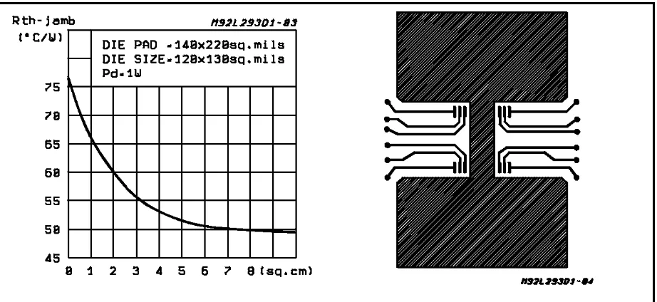
Rth j-amb Thermal Resistance junction-ambient max. 80 50 (*) °C/W
Rth j-case Thermal Resistance Junction-case max. 14 – (*) With 6sq. cm on board heatsink.
PIN CONNECTIONS (Top view)
SO(12+4+4) Powerdip(12+2+2)
L293D - L293DD
ELECTRICAL CHARACTERISTICS (for each channel, VS = 24 V, VSS= 5 V, Tamb = 25°C, unless otherwise specified)
Symbol Parameter Test Conditions Min. Typ. Max. Unit
VS Supply Voltage (pin 10) VSS 36 V
VSS Logic Supply Voltage (pin 20) 4.5 36 V
IS Total Quiescent Supply Current
(pin 10)
Vi= L ; IO= 0 ; Ven= H 2 6 mA
Vi= H ; IO= 0 ; Ven= H 16 24 mA
Ven= L 4 mA
ISS Total Quiescent Logic Supply
Current (pin 20)
Vi= L ; IO= 0 ; Ven= H 44 60 mA
Vi= H ; IO= 0 ; Ven= H 16 22 mA
Ven= L 16 24 mA
VIL Input Low Voltage (pin 2, 9, 12,
19)
– 0.3 1.5 V
VIH Input High Voltage (pin 2, 9,
12, 19)
VSS≤7 V 2.3 VSS V
VSS> 7 V 2.3 7 V
IIL Low Voltage Input Current (pin
2, 9, 12, 19)
VIL= 1.5 V – 10 µA
IIH High Voltage Input Current (pin
2, 9, 12, 19)
2.3 V≤VIH≤VSS– 0.6 V 30 100 µA
Ven L Enable Low Voltage
(pin 1, 11)
– 0.3 1.5 V
Ven H Enable High Voltage
(pin 1, 11)
VSS≤7 V 2.3 VSS V
VSS> 7 V 2.3 7 V
Ien L Low Voltage Enable Current
(pin 1, 11)
Ven L= 1.5 V – 30 – 100 µA
Ien H High Voltage Enable Current
(pin 1, 11)
2.3 V≤Ven H≤VSS– 0.6 V ±10 µA
VCE(sat)H Source Output Saturation
Voltage (pins 3, 8, 13, 18)
IO= – 0.6 A 1.4 1.8 V
VCE(sat)L Sink Output Saturation Voltage
(pins 3, 8, 13, 18)
IO= + 0.6 A 1.2 1.8 V
VF Clamp Diode Forward Voltage IO= 600nA 1.3 V
tr Rise Time (*) 0.1 to 0.9 VO 250 ns
tf Fall Time (*) 0.9 to 0.1 VO 250 ns
ton Turn-on Delay (*) 0.5 Vito 0.5 VO 750 ns
toff Turn-off Delay (*) 0.5 Vito 0.5 VO 200 ns (*) See fig. 1.
L293D - L293DD
TRUTH TABLE (one channel)
Inpu t Enable (*) Output
H L H L
H H L L
H L Z Z
Z = High output impedance
[image:62.595.71.531.95.263.2](*) Relative to the considered channel
Figure 1: Switching Times
Figure 2: Junction to ambient thermal resistance vs. area on board heatsink (SO12+4+4 package)
L293D - L293DD
[image:62.595.68.529.296.508.2]POWERDIP16 PACKAGE MECHANICAL DATA
DIM. mm inch
MIN. TYP. MAX. MIN. TYP. MAX.
a1 0.51 0.020
B 0.85 1.40 0.033 0.055
b 0.50 0.020
b1 0.38 0.50 0.015 0.020
D 20.0 0.787
E 8.80 0.346
e 2.54 0.100
e3 17.78 0.700
F 7.10 0.280
I 5.10 0.201
L 3.30 0.130
Z 1.27 0.050
L293D - L293DD
SO20 PACKAGE MECHANICAL DATA
DIM. mm inch
MIN. TYP. MAX. MIN. TYP. MAX.
A 2.65 0.104
a1 0.1 0.2 0.004 0.008
a2 2.45 0.096
b 0.35 0.49 0.014 0.019
b1 0.23 0.32 0.009 0.013
C 0.5 0.020
c1 45 1.772
D 1 12.6 0.039 0.496
E 10 10.65 0.394 0.419
e 1.27 0.050
e3 11.43 0.450
F 1 7.4 0.039 0.291
G 8.8 9.15 0.346 0.360
L 0.5 1.27 0.020 0.050
M 0.75 0.030
S 8°(max.)
L293D - L293DD
Information furnished is believed to be accurate and reliable. However, SGS-THOMSON Microelectronics assumes no responsibility for the consequences of use of such information nor for any infringement of patents or other rights of third parties which may result from its use. No license is granted by implication or otherwise under any patent or patent rights of SGS-THOMSON Microelectronics. Specification mentioned in this publication are subject to change without notice. This publication supersedes and replaces all information previously supplied. SGS-THOMSON Microelectronics products are not authorized for use as criticalcomponents in life support devices or systems without express written approval of SGS-THOMSON Microelectronics.
1996 SGS-THOMSON Microelectronics – Printed in Italy – All Rights Reserved SGS-THOMSON Microelectronics GROUP OF COMPANIES
Australia Brazil Canada China France Germany Hong Kong Italy Japan Korea Malaysia Malta Morocco The Netherlands -Singapore - Spain - Sweden - Switzerland - Taiwan - Thailand - United Kingdom - U.S.A.
L293D - L293DD
This datasheet has been download from:
www.datasheetcatalog.com
DATA SHEET
Product specification
Supersedes data of September 1994
File under Discrete Semiconductors, SC04
1997 Mar 27
DISCRETE SEMICONDUCTORS
BC556; BC557; BC558
PNP general purpose transistors
book, halfpage
1997 Mar 27 2
Philips Semiconductors Product specification
PNP general purpose transistors
BC556; BC557; BC558
FEATURES
• Low current (max. 100 mA)
• Low voltage (max. 65 V).
APPLICATIONS
• General purpose switching and amplification.
DESCRIPTION
PNP transistor in a TO-92; SOT54 plastic package. NPN complements: BC546, BC547 and BC548.
PINNING
PIN DESCRIPTION
1 emitter
2 base
3 collector
Fig.1 Simplified outline (TO-92; SOT54)
and symbol. handbook, halfpage1
3 2
MAM281
3
2
1
QUICK REFERENCE DATA
SYMBOL PARAMETER CONDITIONS MIN. MAX. UNIT
VCBO collector-base voltage open emitter
BC556 − −80 V
BC557 − −50 V
BC558 − −30 V
VCEO collector-emitter voltage open base
BC556 − −65 V
BC557 − −45 V
BC558 − −30 V
ICM peak collector current − −200 mA
Ptot total power dissipation Tamb≤25°C − 500 mW
hFE DC current gain IC=−2 mA; VCE=−5 V
BC556 125 475
BC557; BC558 125 800
1997 Mar 27 3
Philips Semiconductors Product specification
PNP general purpose transistors
BC556; BC557; BC558
LIMITING VALUES
In accordance with the Absolute Maximum Rating System (IEC 134).
THERMAL CHARACTERISTICS
Note
1. Transistor mounted on an FR4 printed-circuit board.
SYMBOL PARAMETER CONDITIONS MIN. MAX. UNIT
VCBO collector-base voltage open emitter
BC556 − −80 V
BC557 − −50 V
BC558 − −30 V
VCEO collector-emitter voltage open base
BC556 − −65 V
BC557 − −45 V
BC558 − −30 V
VEBO emitter-base voltage open collector − −5 V
IC collector current (DC) − −100 mA
ICM peak collector current − −200 mA
IBM peak base current − −200 mA
Ptot total power dissipation Tamb≤25°C − 500 mW
Tstg storage temperature −65 +150 °C
Tj junction temperature − 150 °C
Tamb operating ambient temperature −65 +150 °C
SYMBOL PARAMETER CONDITIONS VALUE UNIT
1997 Mar 27 4
Philips Semiconductors Product specification
PNP general purpose transistors
BC556; BC557; BC558
CHARACTERISTICS
Tj= 25°C unless otherwise specified.
Notes
1. VBEsat decreases by about−1.7 mV/K with increasing temperature.
2. VBE decreases by about−2 mV/K with increasing temperature.
SYMBOL PARAMETER CONDITIONS MIN. TYP. MAX. UNIT
ICBO collector cut-off current IE= 0; VCB=−30 V − −1 −15 nA
IE= 0; VCB=−30 V; Tj= 150°C − − −4 µA
IEBO emitter cut-off current IC= 0; VEB=−5 V − − −100 nA
hFE DC current gain IC=−2 mA; VCE=−5 V;
see Figs 2, 3 and 4
BC556 125 − 475
BC557; BC558 125 − 800
BC556A; BC557A; BC558A 125 − 250
BC556B; BC557B; BC558B 220 − 475
BC557C; BC558C 420 − 800
VCEsat collector-emitter saturation voltage IC=−10 mA; IB=−0.5 mA − −60 −300 mV
IC=−100 mA; IB=−5 mA − −180 −650 mV
VBEsat base-emitter saturation voltage IC=−10 mA; IB=−0.5 mA; note 1 − −750 − mV
IC=−100 mA; IB=−5 mA; note 1 − −930 − mV
VBE base-emitter voltage IC=−2 mA; VCE=−5 V; note 2 −600 −650 −750 mV
IC=−10 mA; VCE=−5 V; note 2 − − −820 mV
Cc collector capacitance IE= ie= 0; VCB=−10 V; f = 1 MHz − 3 − pF
Ce emitter capacitance IC= ic= 0; VEB=−0.5 V; f = 1 MHz − 10 − pF
fT transition frequency IC=−10 mA; VCE=−5 V; f = 100 MHz 100 − − MHz
F noise figure IC=−200µA; VCE=−5 V; RS= 2 kΩ;
f = 1 kHz; B = 200 Hz
1997 Mar 27 5
Philips Semiconductors Product specification
PNP general purpose transistors
BC556; BC557; BC558
Fig.2 DC current gain; typical values. handbook, full pagewidth
0 300
100 200
MBH726
10−1
hFE
1 10 102 IC (mA) 103
VCE = 5 V
BC556A; BC557A; BC558A.
Fig.3 DC current gain; typical values. handbook, full pagewidth
0 300
200
100
400 MBH727
10−2 10−1
hFE
1 10 102 IC (mA) 103
VCE = 5 V
1997 Mar 27 6
Philips Semiconductors Product specification
PNP general purpose transistors
BC556; BC557; BC558
Fig.4 DC current gain; typical values. handbook, full pagewidth
0 300
200
100 600
500
400
MBH728
10−2 10−1
hFE
1 10 102 IC (mA) 103
VCE = 5 V
1997 Mar 27 7
Philips Semiconductors Product specification
PNP general purpose transistors
BC556; BC557; BC558
PACKAGE OUTLINE UNIT A REFERENCES OUTLINE VERSION EUROPEAN
PROJECTION ISSUE DATE IEC JEDEC EIAJ
mm 5.2 5.0 b 0.48 0.40 c 0.45 0.40 D 4.8 4.4 d 1.7 1.4 E 4.2 3.6 L 14.5 12.7 e 2.54 e1 1.27 L1(1) 2.5 b1 0.66 0.56
DIMENSIONS (mm are the original dimensions)
Note
1. Terminal dimensions within this zone are uncontrolled to allow for flow of plastic and terminal irregularities.
SOT54 TO-92 SC-43 97-02-28
A L
0 2.5 5 mm
scale b c D b1 L1 d E
Plastic single-ended leaded (through hole) package; 3 leads SOT54
e1 e
1997 Mar 27 8
Philips Semiconductors Product specification
PNP general purpose transistors
BC556; BC557; BC558
DEFINITIONS
LIFE SUPPORT APPLICATIONS
These products are not designed for use in life support appliances, devices, or systems where malfunction of these products can reasonably be expected to result in personal injury. Philips customers using or selling these products for use in such applications do so at their own risk and agree to fully indemnify Philips for any damages resulting from such improper use or sale.
Data sheet status
Objective specification This data sheet contains target or goal specifications for product development.
Preliminary specification This data sheet contains preliminary data; supplementary data may be published later.
Product specification This data sheet contains final product specifications.
Limiting values
Limiting values given are in accordance with the Absolute Maximum Rating System (IEC 134). Stress above one or more of the limiting values may cause permanent damage to the device. These are stress ratings only and operation of the device at these or at any other conditions above those given in the Characteristics sections of the specification is not implied. Exposure to limiting values for extended periods may affect device reliability.
Application information
1997 Mar 27 9
Philips Semiconductors Product specification
PNP general purpose transistors
BC556; BC557; BC558
1997 Mar 27 10
Philips Semiconductors Product specification
PNP general purpose transistors
BC556; BC557; BC558
1997 Mar 27 11
Philips Semiconductors Product specification
PNP general purpose transistors
BC556; BC557; BC558
Internet: http://www.semiconductors.philips.com
Philips Semiconductors – a worldwide company
© Philips Electronics N.V. 1997 SCA53
All rights are reserved. Reproduction in whole or in part is prohibited without the prior written consent of the copyright owner.
The information presented in this document does not form part of any quotation or contract, is believed to be accurate and reliable and may be changed without notice. No liability will be accepted by the publisher for any consequence of its use. Publication thereof does not convey nor imply any license under patent- or other industrial or intellectual property rights.
Netherlands: Postbus 90050, 5600 PB EINDHOVEN, Bldg. VB,
Tel. +31 40 27 82785, Fax. +31 40 27 88399
New Zealand: 2 Wagener Place, C.P.O. Box 1041, AUCKLAND,
Tel. +64 9 849 4160, Fax. +64 9 849 7811
Norway: Box 1, Manglerud 0612, OSLO,
Tel. +47 22 74 8000, Fax. +47 22 74 8341
Philippines: Philips Semiconductors Philippines Inc.,
106 Valero St. Salcedo Village, P.O. Box 2108 MCC, MAKATI, Metro MANILA, Tel. +63 2 816 6380, Fax. +63 2 817 3474
Poland: Ul. Lukiska 10, PL 04-123 WARSZAWA,
Tel. +48 22 612 2831, Fax. +48 22 612 2327
Portugal: see Spain Romania: see Italy
Russia: Philips Russia, Ul. Usatcheva 35A, 119048 MOSCOW,
Tel. +7 095 755 6918, Fax. +7 095 755 6919
Singapore: Lorong 1, Toa Payoh, SINGAPORE 1231,
Tel. +65 350 2538, Fax. +65 251 6500
Slovakia: see Austria Slovenia: see Italy
South Africa: S.A. PHILIPS Pty Ltd., 195-215 Main Road Martindale,
2092 JOHANNESBURG, P.O. Box 7430 Johannesburg 2000, Tel. +27 11 470 5911, Fax. +27 11 470 5494
South America: Rua do Rocio 220, 5th floor, Suite 51,
04552-903 São Paulo, SÃO PAULO - SP, Brazil, Tel. +55 11 821 2333, Fax. +55 11 829 1849
Spain: Balmes 22, 08007 BARCELONA,
Tel. +34 3 301 6312, Fax. +34 3 301 4107
Sweden: Kottbygatan 7, Akalla, S-16485 STOCKHOLM,
Tel. +46 8 632 2000, Fax. +46 8 632 2745
Switzerland: Allmendstrasse 140, CH-8027 ZÜRICH,
Tel. +41 1 488 2686, Fax. +41 1 481 7730
Taiwan: Philips Semiconductors, 6F, No. 96, Chien Kuo N. Rd., Sec. 1,
TAIPEI, Taiwan Tel. +886 2 2134 2870, Fax. +886 2 2134 2874
Thailand: PHILIPS ELECTRONICS (THAILAND) Ltd.,
209/2 Sanpavuth-Bangna Road Prakanong, BANGKOK 10260, Tel. +66 2 745 4090, Fax. +66 2 398 0793
Turkey: Talatpasa Cad. No. 5, 80640 GÜLTEPE/ISTANBUL,
Tel. +90 212 279 2770, Fax. +90 212 282 6707
Ukraine: PHILIPS UKRAINE, 4 Patrice Lumumba str., Building B, Floor 7,
252042 KIEV, Tel. +380 44 264 2776, Fax. +380 44 268 0461
United Kingdom: Philips Semiconductors Ltd., 276 Bath Road, Hayes,
MIDDLESEX UB3 5BX, Tel. +44 181 730 5000, Fax. +44 181 754 8421
United States: 811 East Arques Avenue, SUNNYVALE, CA 94088-3409,
Tel. +1 800 234 7381
Uruguay: see South America Vietnam: see Singapore
Yugoslavia: PHILIPS, Trg N. Pasica 5/v, 11000 BEOGRAD,
Tel. +381 11 625 344, Fax.+381 11 635 777
For all other countries apply to: Philips Semiconductors, Marketing & Sales Communications,
Building BE-p, P.O. Box 218, 5600 MD EINDHOVEN, The Netherlands, Fax. +31 40 27 24825
Argentina: see South America
Australia: 34 Waterloo Road, NORTH RYDE, NSW 2113,
Tel. +61 2 9805 4455, Fax. +61 2 9805 4466
Austria: Computerstr. 6, A-1101 WIEN, P.O. Box 213,
Tel. +43 1 60 101, Fax. +43 1 60 101 1210
Belarus: Hotel Minsk Business Center, Bld. 3, r. 1211, Volodarski Str. 6,
220050 MINSK, Tel. +375 172 200 733, Fax. +375 172 200 773
Belgium: see The Netherlands Brazil: see South America
Bulgaria: Philips Bulgaria Ltd., Energoproject, 15th floor,
51 James Bourchier Blvd., 1407 SOFIA, Tel. +359 2 689 211, Fax. +359 2 689 102
Canada: PHILIPS SEMICONDUCTORS/COMPONENTS,
Tel. +1 800 234 7381
China/Hong Kong: 501 Hong Kong Industrial Technology Centre,
72 Tat Chee Avenue, Kowloon Tong, HONG KONG, Tel. +852 2319 7888, Fax. +852 2319 7700
Colombia: see South America Czech Republic: see Austria
Denmark: Prags Boulevard 80, PB 1919, DK-2300 COPENHAGEN S,
Tel. +45 32 88 2636, Fax. +45 31 57 1949
Finland: Sinikalliontie 3, FIN-02630 ESPOO,
Tel. +358 9 615800, Fax. +358 9 61580/xxx
France: 4 Rue du Port-aux-Vins, BP317, 92156 SURESNES Cedex,
Tel. +33 1 40 99 6161, Fax. +33 1 40 99 6427
Germany: Hammerbrookstraße 69, D-20097 HAMBURG,
Tel. +49 40 23 53 60, Fax. +49 40 23 536 300
Greece: No. 15, 25th March Street, GR 17778 TAVROS/ATHENS,
Tel. +30 1 4894 339/239, Fax. +30 1 4814 240
Hungary: see Austria
India: Philips INDIA Ltd, Shivsagar Estate, A Block, Dr. Annie Besant Rd.
Worli, MUMBAI 400 018, Tel. +91 22 4938 541, Fax. +91 22 4938 722
Indonesia: see Singapore
Ireland: Newstead, Clonskeagh, DUBLIN 14,
Tel. +353 1 7640 000, Fax. +353 1 7640 200
Israel: RAPAC Electronics, 7 Kehilat Saloniki St, TEL AVIV 61180,
Tel. +972 3 645 0444, Fax. +972 3 649 1007
Italy: PHILIPS SEMICONDUCTORS, Piazza IV Novembre 3,
20124 MILANO, Tel. +39 2 6752 2531, Fax. +39 2 6752 2557
Japan: Philips Bldg 13-37, Kohnan 2-chome, Minato-ku, TOKYO 108,
Tel. +81 3 3740 5130, Fax. +81 3 3740 5077
Korea: Philips House, 260-199 Itaewon-dong, Yongsan-ku, SEOUL,
Tel. +82 2 709 1412, Fax. +82 2 709 1415
Malaysia: No. 76 Jalan Universiti, 46200 PETALING JAYA, SELANGOR,
Tel. +60 3 750 5214, Fax. +60 3 757 4880
Mexico: 5900 Gateway East, Suite 200, EL PASO, TEXAS 79905,
Tel. +9-5 800 234 7381
Middle East: see Italy
This datasheet has been download from:
www.datasheetcatalog.com
BAB I
PENDAHULUAN
I.1. Latar Belakang
Saat ini teknologi robot berkembang dengan cepat. Robot dapat digunakan untuk: 1) membantu meringankan pekerjaan manusia, terutama jenis pekerjaan yang membutuhkan ketelitian serta daya tahan dalam jangka waktu yang lama, 2) menggantikan manusia melakukan pekerjaan yang memiliki resiko atau bahaya yang besar dan 3) menjangkau daerah-daerah tertentu yang tidak dapat dijelajahi oleh manusia. Penggunaan robot tersebut banyak ditemui di dalam berbagai bidang seperti: bidang kedokteran, bidang industri, eksplorasi ruang angkasa dan lain sebagainya, baik dalam bentuk penelitian ataupun proses produksi.
Salah satu jenis robot yang banyak dipakai di dalam bidang industri adalah robot yang dapat mengikuti lintasan garis tertentu (line follower
robot). Robot jenis ini pada umumnya berbentuk kendaraan seperti: mobil.
Robot ini menggunakan sensor photo-reflector atau sensor image untuk mendeteksi lintasan yang harus diikuti dan motor sebagai komponen penggeraknya. Untuk mengendalikan pergerakkan robot tipe ini dapat menggunakan beberapa metoda kendali seperti metoda PID, logika fuzzy, jaringan saraf tiruan dan lain-lain. Beberapa contoh aplikasi robot jenis ini yaitu: 1) trayek angkutan dalam skala kecil, misal di rumah sakit sehingga pasien tidak perlu berjalan untuk sampai ke tempat yang dituju, 2) untuk sistem pengantaran barang dari satu bagian produksi ke bagian produksi yang lain, 3) dapat digunakan sebagai media reklame iklan berjalan di mal-mal atau pusat perbelanjaan.
Universitas Kristen Maranatha
Bab I - Pendahuluan 2
I.2. Identifikasi Masalah
Identifikasi masalah yang dilakukan adalah bagaimana merancang dan merealisasikan kendaraan yang mengikuti suatu lintasan tertentu dengan pengendali logika fuzzy?
I.3. Tujuan
Sesuai dengan judul tugas akhir ini, penulis bertujuan untuk merancang serta merealisasikan kendaraan yang mengikuti suatu lintasan tertentu dengan pengendali logika fuzzy.
I.4. Spesifikasi Alat
1. Mikrokontroler yang digunakan adalah tipe ATMega16 dari keluarga AVR Atmel.
2. Sensor inframerah yang digunakan untuk mendeteksi lintasan yang harus diikuti adalah sensor optocoupler tipe GP2S28 sebanyak enam buah.
3. Motor DC 12 volt sebanyak dua buah.
4. Menggunakan IC driver L293D untuk men-drive motor dc 12 volt.
5. Roda yang dipakai sebanyak empat buah, dengan komposisi dua buah roda bergerak dan dua roda statis.
I.5. Pembatasan Masalah
Untuk lebih mengarahkan pembahasan, maka tugas akhir ini dilaksanakan dalam batas-batas sebagai berikut:
1. Robot ini merupakan jenis rover yang bergerak maju mengikuti bentuk dari lintasan tertutup.
2. Jalur yang ditempuh rata, tidak ada rintangan serta halangan seperti tanjakan, lubang, benda dan lain-lain.
3. Warna bidang alas yang dipakai adalah warna putih dan garis lintasan yang dipakai warna hitam.
4. Robot ini menggunakan penjejakan sensor inframerah.
Bab I - Pendahuluan 3 5. Kecepatan putar dari motor dc kiri dan kanan diabaikan.
Karena yang diperhatikan adalah lamanya motor dc bekerja yang diatur dengan metoda PWM (Pulse Width Modulation). 6. Mekanisme pergerakan robot untuk berbelok kiri dan kanan
diatur dengan mengendalikan kecepatan putar dari roda kiri dan roda kanan.
I.6. Sistematika Penulisan
Laporan Tugas Akhir ini terdiri atas 5 bab dengan sistematika penulisan sebagai berikut :
Bab I Pendahuluan
Pada bab ini dipaparkan mengenai latar belakang masalah, identifikasi masalah, tujuan penulisan, spesifikasi alat, pembatasan masalah, dan sistematika penulisan laporan.
Bab II Landasan Teori
Pada bab ini dibahas mengenai teori dasar dari robot, sensor
inframerah, logika fuzzy dan mikrokontroler AVR ATMega16.
Bab III Perancangan Dan Realisasi Perangkat Keras Dan Lunak
Pada bab ini dipaparkan mengenai perancangan dan realisasi, baik perangkat keras dan perangkat lunak dari kendaraan yang mengikuti suatu lintasan tertentu. Perangkat lunak yang dibahas dibagi dua, yang pertama dalam bahasa asember untuk mikrokontroler dan yang kedua perancangan logika fuzzy yang digunakan dengan menggunakan software petrafuz.
Bab IV Data Pengamatan Kendaraan Yang Mengikuti Suatu Lintasan Tertentu
Pada bab ini dibahas mengenai hasil data pengamatan yang didapat dari percobaan. Data pengamatan yang didapat dibagi menjadi beberapa bagian: yang pertama data pembacaan
Bab I - Pendahuluan 4 sensor kendaraan terhadap bidang dan garis lintasan dengan satu, tiga dan enam sensor menyala semua. Yang kedua data
input dan output hasil simulasi logika fuzzy dengan software
petrafuz dan yang ketiga data pengamatan gerak kendaraan dalam mengikuti garis lintasan.
Bab V Kesimpulan Dan Saran
Pada bab ini dipaparkan kesimpulan yang diambil berdasarkan data pengamatan hasil gerak kendaraan dan simulasi logika
fuzzy serta saran-saran untuk pengembangan lebih lanjut.
BAB V
KESIMPULAN DAN SARAN
Kesimpulan
1) Realisasi kendaraan yang mengikuti suatu lintasan berwarna hitam pada bidang dasar berwarna putih, secara hardware menggunakan mikrokontroler ATMega16 berhasil dibuat.
Saran
Ada beberapa saran yang dapat dilakukan untuk memperbaiki atau meningkatkan kerja sistem kendaraan yang mengikuti suatu lintasan tertentu, yaitu:
1) Hasil realisasi software dalam TA ini belum da