Annealing Effects on Silica Based Optical Waveguides
Fabricated by Electron Beam Irradiation
Ary Syahriar
Program Studi Teknik Elektro, Fakultas Sains dan Teknologi, Universitas Al Azhar Indonesia, Jl. Sisingamangaraja, Jakarta 12110
E-mail: [email protected]
Abstract – Defect in channel waveguide fabricated by e-beam irradiation of PECVD silica-on-silicon films are analyzed by characterizing the propagation constant change due to high temperature annealing. The changes of normalized compaction are also described and the theoretical prediction on the variation of normalized compaction with anneal temperature in isochronal annealing is also provided.
Keywords – optical communications, optical waveguides, directional coupler, straight waveguides, silica on silicon
I. INTRODUCTION
uring the past few decades, the structures of silica glass have been extensively researched. This work has been driven partly by the continuing optimization of silica glasses used in traditional applications, but mainly the rapid expansions of silica based optical communications and MOS electronic devices.
Defects center in silica glasses affect performance in optical and electronic applications, in that they introduce optical absorption and charge trapping. The electronic structure of defect centers in amorphous silica has been extensively studied using techniques such as optical absorption spectroscopy [1], luminescent spectroscopy [2], capacitance-voltage (C-V) characterization of MOS devices [3], and electron spin resonance [4].
Optical absorption spectroscopy may be used to study defect centers since the different centers absorb different wavelengths of light. For example the NBOHC center absorbs wavelengths of around
630 nm (red) whereas the E’ center absorbs
wavelengths of around 215 nm (UV). This method
is only limited by the sensitivity with which optical absorption may be measured and hence is of most use with high irradiation dose, or long path length samples (such as optical fibers). Its advantages include that it is inexpensive and that the luminescent spectroscopy methods have similar advantages and disadvantages.
Electron spin resonance spectroscopy is a powerful tool and can be used to identify the atomic structure of new defects. It is based on the Zeeman Effect whereby the spin state of a lone electron in a defect may be separated by subjecting the sample to a strong magnetic field. Transition between these spin states can then be induced by the application of a microwave signal of an appropriate energy. The present of an absorption peak when the magnetic field or microwave frequency is scanned therefore provides evidence of a defect. The magnetic field and microwave frequency combination at the peak, together with the shape of the peak, provide evidence of the type of defect present, since these parameters are affected by the environment of the lone electron (i.e. the neighboring atoms). This method cannot, however, be used to identify diamagnetic (non paramagnetic) defects, i.e. defects without lone electron. Electrical characterization techniques are used to investigate the radiation-induced charging effects in MOS structures, since such effects may adversely affect the performance of devices containing such structures.
II. EXPERIMENTAL SETUP
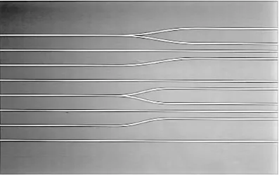
Figure 1 shows a set of typical devices, which comprised straight waveguides, back-to-back S-bends, and Mach-Zehnder interferometers. This picture was taken directly from the mask plate used to pattern the waveguide structures. Each S-bend has a constant lateral offset l and a different transition length L.
The Mach-Zehnder interferometers were also constructed using similar sinusoidal bend shapes, which were simply reflected and overlaid one upon another to yield the desired interferometer structure. In the experiments, all the waveguide bends were made with a fixed offset of l =150 m and a length L varying between 1 mm and 6 mm. The overall chip length was 3.4 cm. Parameters were chosen for a low loss coupling to a single-mode optical fibre, with a guide width of 7 m. The energy used for the irradiation was 25 keV, and the charge dose was 0.74 C/cm2. The apparatus for a single-point measurement of optical insertion loss is shown in Figure 2.
The illustration shows the laser (wavelength of 1.523 m) launched into a standard 8/125 m single mode fibre. A broad-band fused coupler provided a reference to allow compensation for variations in laser output [5]. A /2 plate was used to rotate the polarization, so that TE and TM modes could both be launched. All the waveguides were single-moded. Two detectors and two lock-in amplifiers were used, and the transmitted intensity was normalized to the direct laser output.
The fibre-device-fibre insertion losses were measured with manually optimized butt-coupling between the fibre and the devices. The exposed surface of the waveguide was covered by a layer of oil with a refractive index of 1.43. Figure 3 shows measurements of TE and TM loss in waveguide bends made on BNR PECVD material that had been subjected to two different treatments
The first set of data were measured using material which had simply been irradiated. The second sets of measurements were made using a similar material, which was annealed in oxygen at 800oC for 30 seconds after irradiation.
In each case, losses are relatively low at large transition lengths; rising abruptly as the transition length (and thus the minimum radius) is reduced. The transition length that may be tolerated is clearly lower after annealing.
Figure 1. Photograph of the mask used to generate the waveguide structures used in the experiments
Lock-in A Lock-in B
He-Ne LD
plate Alignment
microscope
Fused 3 dB coupler Waveguide
sample
Ratiometer
Ge photodiodes 1.525 µm
Output
Figure 2. The experimental set-up used to measure
optical insertion loss, after reference [5] Figure 3. The measurement of TE and TM loss of back-to-back S-bends of different transition lengths 0
5 10 15 20 25 30
1 2 3 4 5 6
Transition length L (mm)
L
o
s
s
(
d
B
)
.
annealed 800 oC, 30 sec
Un-annealed TE Mode
TM Mode L
III.METHODOLOGY
The macroscopic effects of irradiation in silica glass, such as volumetric and refractive index changes are caused by the formation of defects. Their subsequent relaxation is in turn due to the reaction with diffusing molecular species [5][6]. A number of defects may be created; those that are paramagnetic have been identified by electron spin resonance [7]. Their relative concentrations vary from material to material, depending on the initial precursor existing in the material.
There are three possible mechanisms for induced irradiation index changes [8][9]. The first is the liberation of molecular species, which diffuse through the silica lattice and escape. The main evidence for this effect is the liberation of hydrogen molecules on irradiation [6]. It cannot, however, be the major contributor to the refractive index change since a substantial reduction in hydrogen contamination was achieved by thermal annealing prior to irradiation, without reducing the index change [5]. Another possibility is the relaxation of strained bonds, but this is also unlikely, as the annealing treatment was performed over a wide range of temperatures.
The most plausible mechanism is the creation of defects from precursors that already exist in the silica layers. However, defect creation may also occur due to the intense ion bombardment and simultaneous UV radiation exposure during deposition. Additionally there is no general way to estimate the defect creation during deposition since the UV radiation present in a reactor depends upon many parameters such as reactor geometry, excitation power, gas used, etc. [9]. Consequently, it is very difficult to determine the form of defect that exists inside the film.
Three main types of paramagnetic defects have
been identified namely: E’ (E prime), peroxy
radical and non-bridging oxygen hole centre (NBOH) defects [10][11]. The most detailed information on defect structures in silica glass has been reviewed by Warren et al. [12]. The influences
of thermal annealing on irradiation induced E’
centers in silica glassalso has been studied in [13]. The study of thermal fiber annealing effect in interferometric fiber-optic current sensor is presented in [14].
The E’ defect has been identified as an SiO3 moiety (where the three parallel lines represent
three separate bonds to oxygen and the dot denotes an unpaired electron), with an unpaired electron in a dangling sp3 orbital of a silicon atom bonded to three oxygen atoms [15][10]. This defect introduces an ultraviolet absorption band at 5.77 eV (215 nm), and a refractive index change at visible and IR wavelengths [4.2]. Recently, nine slightly different
kinds of E’ defect centre have been separately
identified in different forms of silica. The precursor
of all E’ defects is assumed to be the oxygen
vacancy (O3SiSiO3), although another possibility is a strained cyclic trisiloxane.
The NBOH centre can be produced in high-OH silica as well as in low-OH silica [16]. It consists of
oxygen (O3SiO), which introduces visible absorption bands at 2.00 eV (630 nm) and 1.63 eV (760 nm). Its precursor is most likely the hydroxyl group (O3SiOH). These defects can all be created by exposure to neutron, electron, -ray, X-ray and UV radiation. However, the actual amount of radiation needed depends on the material.
Characterization of the contribution of different defects to waveguide performance requires a correlation between either volumetric or refractive index changes and the defect density. Theoretically, the defect density might be observed by electron spin resonance methods, but since the induced changes occur in waveguide geometry, it is very difficult to separate the various contributions to loss over the required range of dose in a spectroscopy experiment [5].
As we have shown, annealing of irradiated silica waveguides will result in a gradual reduction in the irradiation-induced index change. This process is thought to take place through reactions with molecular species that diffuse from interstitial sites [11]. The reaction, however, can involve defect transformation: for example, peroxy radicals can be formed by E’ reaction with O2, or new products may be produced such as silicon hydride. The kinetics of annealing is therefore very complicated, since both diffusion and reaction steps are involved.
Annealing prior to irradiation also contributes to more complicated defect creation. According to [16], pre-annealing increases the E’ centre density by a factor of at least 20 in BNR material, which implies that annealing must either increase the density of precursors or the stability of the resulting
800 decay of the induced changes during post-annealing at constant temperature will follow a simple exponential function. For example, irradiation induced compaction and index changes both follow the law [5]: expected to follow [5]:
1 1 activation energy for the annealing reaction.
IV.RESULT AND DISCUSSION
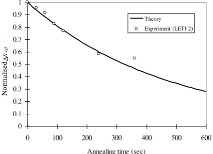
Figure 4 shows the variation of neff(normalized to
neffinitial) with annealing time, fitted to Equation
(4.2). It shows that the simple exponential approximation is in good agreement with the experimental data, and that the change in neffdoes
indeed vary as expected [17].
Figure 4. Variation of neff with annealing time for the LETI 2 sample at high temperature of 800 oC. The theoretical fit of Equation (1) is shown for comparison
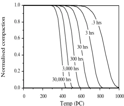
In a similar way, Figure 5 shows the variation of normalized compaction at the edge of a planar guide for a number of different temperatures [5]. In each case, the decay of the induced change is also waveguide during any further post-processing effect could be estimated. Figure 7 illustrates the theoretical estimation of normalized compaction versus process temperature for times ranging from 0,3-30 000 hours.
1000
Figure 7. Theoretical prediction of the variation of normalised compaction with anneal temperature in isochronal annealing
The result suggests that indefinite operation at room temperature, or further post-processing at 350oC for limited time, would be possible [5]. Therefore, post-processing of irradiated waveguides without changing the waveguide characteristics should be possible, for example using a low-temperature PEVD process to deposit the cladding layer. However, this LETI material was actually the most stable of any of the similar PECVD films investigated at Imperial College. As we have shown, waveguide devices formed in BNR material are considerably less stable, thus increasing the difficulty of identifying a suitable over cladding process.
V. CONCLUSIONS
Furthermore, the effects of post-process isothermal annealing on irradiated waveguides have also been assessed by analyzing the change of the effective index of the guide. The results show that annealing increases the losses in the waveguide bends and the coupling coefficient of directional couplers. These effects are due to a decrease in the value of neff
which follows from the annealing of the defects existing inside the silica layer. However, a direct relation between annealing process and the refractive index change is unclear, and has been found to vary from material to material.
The effective index decay poses major problems for further processing, such as the deposition of the cladding layer needed to isolate the guided mode from the heater electrode in a thermo optic switch. However, we have predicted that this step may be
successfully performed providing a suitably low-temperature process is used.
REFERENCES
[1] D.L. Griscom., “Defect structure of glasses. Some
outstanding question with regard to vitreous silica”,
J. Non-Cryst. Sol. Vol 73, 51-77, 1985.
[2] H. Koyama, “Cathode luminescence study of
SiO2”, J. Appl. Phys, vol 51, 2228-2235, 1980.
[3] W.L. Warren, P.M. Lenahan, B. Robinson, J.H.
Stathis., “Neutral E’ centers in microwave
downstream plasma-enhanced chemical-vapor
deposited silicon dioxide”’ Alll. Phys. Lett, vol 53,
482-484, 1988.
[4] E.H. Pointdexter, P.J. Caplan, “Characterisation of Si/SiO2 interface defects by electron spin
resonance”, Progress in surface science, vol 14,
201-209, 1983.
[5] R.R.A. Syms, T.J. Tate, J.J. Lewandowski, “Near
-infrared channel waveguides formed by electron-beam irradiation of silica layers on silicon
substrates”, IEEE J. Lightwave Technol., vol. LT
-12, 2085-2091, 1994.
[6] R.A.B. Devine, “Macroscopic and microscopic
effects of radiation in amorphous SiO2 ”, Nucl.
Instrum. and Meth. In Phys. Res. vol. B91, 378-390, 1994.
[7] S.M.R. Spaargaren, “Radiation effects in silica
based waveguides”, Ph.D. Thesis. University of
London, 1998.
[8] D.L. Griscom, “Defect structure of glasses”, J. of
Non-crystalline Solids, vol. 73, 51-77, 1985.
[9] R.A.B. Devine, “On the physical models of
annealing of radiation induced defects in amorphous SiO2”, Nucl. Instrum. and Meth. in
Phys. Res. vol. B46, 261-264, 1990.
[10] R.A.B. Devine, “Radiation induced structural
changes in amorphous SiO2: I. Point defects”, Jpn.
J. Appl. Phys., vol. 31, 4411-4421, 1992.
[11] S.P. Faile, D.M. Roy, “Mechanism of color center destruction in hydrogen impregnated radiation
resistant glasses”, Mat. Res. Bull., vol. 5, 385-390,
1970.
[12] W.L. Warren, E.H. Poindexter, M. Offenberg, W. Muller-Warmuth, “Paramagnetic point defects in amorphous silicon dioxide and amorphous silicon
nitride thin film”, J. Electrochem. Soc., vol. 139,
872-880, 1992.
[13] T. Wang, Z.Xiao, W. Luo, “The influences of
thermal annealing temperatures on irradiation
induced E’ centers in silica glass”, IEEE
Transactions on Nuclear Science, Vol.55, 2685-2688, 2008.
[14] M. Lenner, R. Wüest, A. Frank, K. Bohnert,
“Effects of thermal fiber annealing on the
temperature compensation of interferometric
[15] J. Lewandowski, R.R.A. Syms, M.Grant, S. Bailey,
“Controlled formation of buried-channel
waveguides by electron beam irradiation of glassy
layers on silicon”, Int. J. of. Optoelectron., vol. 9,
143-149, 1994.
[16] T. Erdogan, V. Mizrahi, P.J. Lemaire, D. Monroe,
“Decay of ultraviolet- induced fiber Bragg
gratings”, J. Appl. Phys., vol. 76, 73-80, 1994.
[17] S. Kannan, J.Z.Y. Guo, P.J. Lemaire, “Thermal