August 1984
The MM74HC4066 devices are digitally controlled analog switches utilizing advanced silicon-gate CMOS technology. These switches have low “ON” resistance and low “OFF” leakages. They are bidirectional switches, thus any analog input may be used as an output and visa-versa. Also the MM74HC4066 switches contain linearization circuitry which lowers the “ON” resistance and increases switch lin-earity. The MM74HC4066 devices allow control of up to 12V (peak) analog signals with digital control signals of the same range. Each switch has its own control input which disables each switch when LOW. All analog inputs and out-puts and digital inout-puts are protected from electrostatic damage by diodes to VCC and ground.
Features
■Typical switch enable time: 15 ns ■Wide analog input voltage range: 0–12V ■Low “ON” resistance: 30 typ. (MM74HC4066) ■Low quiescent current: 80 µA maximum (74HC) ■Matched switch characteristics
■Individual switch controls
Ordering Code:
Devices also available in Tape and Reel. Specify by appending the suffix letter “X” to the ordering code. Pb-Free package per JEDEC J-STD-020B.
Schematic Diagram
MM74HC4066M M14A 14-Lead Small Outline Integrated Circuit (SOIC), JEDEC MS-012, 0.150" Narrow MM74HC4066MX_NL M14A Pb-Free 14-Lead Small Outline Integrated Circuit (SOIC), JEDEC MS-012, 0.150" Narrow MM74HC4066SJ M14D Pb-Free 14-Lead Small Outline Package (SOP), EIAJ TYPE II, 5.3mm Wide
MM74HC4066MTC MTC14 14-Lead Thin Shrink Small Outline Package (TSSOP), JEDEC MO-153, 4.4mm Wide MM74HC4066N N14A 14-Lead Plastic Dual-In-Line Package (PDIP), JEDEC MS-001, 0.300" Wide
Input Switch
CTL I/O–O/I
L “OFF”
M
M
74HC4066
(Note 2)
Conditions
Note 1: Absolute Maximum Ratings are those values beyond which dam-age to the device may occur.
Note 2: Unless otherwise specified all voltages are referenced to ground.
Note 3: Power Dissipation temperature derating — plastic “N” package: −
12 mW/°C from 65°C to 85°C.
DC Electrical Characteristics
(Note 4)Note 4: For a power supply of 5V ±10% the worst case on resistance (RON) occurs for HC at 4.5V. Thus the 4.5V values should be used when designing with
this supply. Worst case VIH and VIL occur at VCC = 5.5V and 4.5V respectively. (The VIH value at 5.5V is 3.85V.) The worst case leakage current occurs for
CMOS at the higher voltage and so the 5.5V values should be used.
Note 5: At supply voltages (VCC–GND) approaching 2V the analog switch on resistance becomes extremely non-linear. Therefore it is recommended that
these devices be used to transmit digital only when using these supply voltages.
Supply Voltage (VCC) −0.5 to +15V
Power Dissipation (PD)
(Note 3) 600 mW
S.O. Package only 500 mW
Lead Temperature (TL)
(Soldering 10 seconds) 260°C
Min Max Units
Supply Voltage (VCC) 2 12 V
DC Input or Output Voltage
(VIN, VOUT) 0 VCC V
Operating Temperature Range (TA) −40 +85 °C
Input Rise or Fall Times
(tr, tf) VCC = 2.0V 1000 ns
Input Voltage 4.5V 3.15 3.15 3.15 V
9.0V 6.3 5.3 6.3 V
12.0V 8.4 8.4 8.4 V
VIL Maximum LOW Level 2.0V 0.5 0.5 0.5 V
Input Voltage 4.5V 1.35 1.35 1.35 V
MM74HC4066
tPHL, tPLH Maximum Propagation 2.0V 25 50 30 75 ns
Delay Switch In to Out 4.5V 5 10 13 15 ns
Feedthrough V(CT)VIL
Isolation (Note 7) (Note 8) 4.5V −42 dB
CIN Maximum Switch 20 pF
Input Capacitance
CIN Maximum Feedthrough VCTL = GND 0.5 pF
Capacitance
CPD Power Dissipation 15 pF
M
M
74HC4066
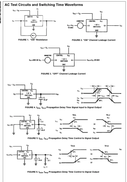
FIGURE 1. “ON” Resistance FIGURE 2. “ON” Channel Leakage Current
FIGURE 3. “OFF” Channel Leakage Current
FIGURE 4. tPHL, tPLH Propagation Delay Time Signal Input to Signal Output
FIGURE 5. tPZL, tPLZ Propagation Delay Time Control to Signal Output
MM74HC4066
AC Test Circuits and Switching Time Waveforms
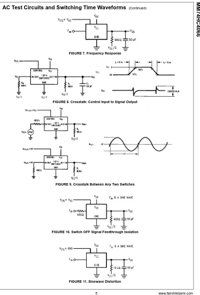
(Continued)FIGURE 7. Frequency Response
FIGURE 8. Crosstalk: Control Input to Signal Output
FIGURE 9. Crosstalk Between Any Two Switches
M
M
74HC4066
Typical “ON” Resistance Typical Crosstalk BetweenAny Two SwitchesTypical Frequency Response
Special Considerations
In certain applications the external load-resistor current may include both VCC and signal line components. To
avoid drawing VCC current when switch current flows into
MM74HC4066
Physical Dimensions
inches (millimeters) unless otherwise notedM
M
74HC4066
MM74HC4066
Physical Dimensions
inches (millimeters) unless otherwise noted (Continued)MM74HC4066 Quad
Anal
og Sw
it
c
Physical Dimensions
inches (millimeters) unless otherwise noted (Continued)14-Lead Plastic Dual-In-Line Package (PDIP), JEDEC MS-001, 0.300" Wide Package Number N14A
Fairchild does not assume any responsibility for use of any circuitry described, no circuit patent licenses are implied and Fairchild reserves the right at any time without notice to change said circuitry and specifications.
LIFE SUPPORT POLICY
FAIRCHILD’S PRODUCTS ARE NOT AUTHORIZED FOR USE AS CRITICAL COMPONENTS IN LIFE SUPPORT DEVICES OR SYSTEMS WITHOUT THE EXPRESS WRITTEN APPROVAL OF THE PRESIDENT OF FAIRCHILD SEMICONDUCTOR CORPORATION. As used herein:
1. Life support devices or systems are devices or systems which, (a) are intended for surgical implant into the body, or (b) support or sustain life, and (c) whose failure to perform when properly used in accordance with instructions for use provided in the labeling, can be rea-sonably expected to result in a significant injury to the user.
2. A critical component in any component of a life support device or system whose failure to perform can be rea-sonably expected to cause the failure of the life support device or system, or to affect its safety or effectiveness.