Study of Suspension Concentration Effect to The Electrical
Resistance of Zinc Sulphophthalocyanine (ZnPcS
n) Thin Film as
Prototype of Ozone Detector
Dhesy Galuh Ratnawati1*, Masruroh2, Rachmat Triandi Tjahjanto1
1
Departement of Chemistry, Faculty of Science, Brawijaya University, Jl. Veteran 65145, Malang, East Java, Indonesia
2
Departement of Physics, Faculty of Science, Brawijaya University, Jl. Veteran 65145, Malang, East Java, Indonesia
*Corresponding author: [email protected]
Received 2 December 2013; Accepted 10 April 2014; Published online for edition May-August 2014
ABSTRACT
We have studied the fabrication of zinc sulphophthalocyanine (ZnPcSn) thin film as prototype of ozone detector. The aim of this research is to find the relation between the electrical resistance of ZnPcSn thin film and the ZnPcSn suspension concentration. The thin film of ZnPcSn was deposited on Printed Circuit Board (PCB) substrate by using spin coating method, then, annealed at temperature of 100 oC. The resistance of ZnPcSn thin film was measured as it was exposed with ozone, synthesized from fresh air, for 60 min continuously. The electrical measurement was conducted twice for each point of data. The result of this research shows that the electrical resistance of ZnPcSn thin film decreases during the ozone exposure, and, it can be concluded that as the concentration of ZnPcSn suspension concentration increase, more amount of ozone can be adsorbed by thin film.
Keywords: zinc sulphophthalocyanine (ZnPcSn) thin film, PCB substrate, suspension concentration, ozone, electrical resistance
INTRODUCTION
The general method to detect ozone is the sensor-based method, for example, solid electrolyte, wet electrochemical sensor and metal oxides sensor. The solid electrolyte sensor is used to control the exhaust gas by using electrolyte cell plate insulated by two electrodes [1] which is operated only at high temperature [2]. The wet electrochemical sensor is gas sensor also use an electrochemical principle for gas detection. This method exhibits high sensitivity towards gases and requires less cost but with complexity of the maintenance [3]. Metal oxides sensor such as SnO2, In2O3 dan WO3, doped or undoped, can be used to detect
CO, NOx and O3 gases [2]. This sensor needs catalyst and high temperature to work [4].
Another method that used for gas detection is utilizing organic semiconductors as sensors, one of them is metal phthalocyanine thin film.
We studied the fabrication of zinc phthalocyanine (ZnPc) thin film on a commercially available circuit board. ZnPc is relatively cheap and having a good sensitivity toward gases up to ppb level [5]. In addition, modified ZnPc has been widely developed as oxidizing gas sensor like NO2 [6], but the usage as ozone sensor was not reported yet. Therefore, in this
ZnPc is less soluble either in organic solvent or in water [7] and tends to aggregate [8, 9]. Therefore, the structure of ZnPc needs to be modified to increase its solubility [7, 8]. Modification can increase the distance of Van der Waals interaction between planar macrocyclic ring of ZnPc, thereby the solvation is easier [9, 10]. We modified ZnPc by adding sulphonyl substituent through sulphonation reaction because of practical consideration. The addition is expected to increase the solubility of ZnPc in organic solvent.
ZnPcSn thin film is deposited on interdigitated pattern electrode. This pattern can
prevent cracking of the thin film, produce smooth and homogenous thin film and exhibit high conductivity between electrodes [5]. The commonly used-electrode for thin film deposition is Au or Pt electrode deposited on glass or alumina substrate [2, 5, 11], but it requires more cost and complex fabrication. Therefore, PCB is used in this research because it is cheap, can be formed to appropriate electrode design easily and conduct the electricity effectively with dielectric constant for approximately 2.3 [12].
The general methods for thin film deposition of less soluble metal phthalocyanine in organic solvent are spin coating, dip coating and sol-gel [13]. This research focus on the spin coating method as a deposition method, because it is easy to be applied and capable of producing continuous and smooth thin film [14]. The resulted ZnPcSn thin film are observed
for their surface morphology and measured for their electrical resistance. In this paper, we also report the effect of concentration ZnPcSn suspension to the electrical resistance of thin
film as ozone detector.
EXPERIMENT
Materials and chemicals
Zinc phthalocyanine (ZnPc) containing with 97% dye content was purchased from Sigma Aldrich Company (Singapore) and is used without further purification. The electrode is copper curves made from a commercially available PCB for electronic device. Material used for etching of PCB is iron(III) chloride (FeCl3) of technical grade and purchased from
Merck (Germany). Another chemical used in this experiment are H2SO4 96% (w/v),
methanol, acetone, and chloroform. All chemical are of analytical grade and purchased from Merck (Germany).
Apparatus
Apparatus used for deposition of thin film is vacuum spin coater VTC-100. The other apparatus used in this research are homemade ozone generator, HF-10 Digital Flow Checker, Mettler PE 300 analytical balance, hotplate with magnetic stirrer IKAMAG®RH, optical microscope Olympus BX-53, Scanning Electron Microscopy (SEM) Hitachi TM3000 Tabletop Microscope, electric shaker WiseShake®SHO-2D, multimeter HELES UX878TR, ultrasonic bath BRANSON 2210, micropipette, set of reflux apparatus, glassware, universal indicator Merck and oven Fischer Scientific.
Synthesis of Zinc Sulphophthalocyanine (ZnPcSn)
Thereafter, pH of the mixture was adjusted to pH 7-7.9 and the color of solution become deep blue. The solvent of the mixture was evaporated and the resulting solid was dissolved in 125 ml NaOH 0.1 M while being stirred by magnetic stirrer. After that, 125 ml HCl 0.1 M was added to precipitate zinc sulphophthalocyanine (ZnPcSn). Finally, ZnPcSn was filtered
with filter paper and the filter cake was dried in oven at 100 oC to a constant weight.
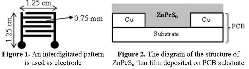
Fabrication of Electrode on PCB Substrate
The interdigitated pattern was designed using computer program at size of 1.25 x 1.25 cm as shown in Figure 1. The printed pattern was transferred onto the copper
layer of a PCB by using a hot iron with hand pressure. Subsequently, PCB with interdigitated pattern was etched in 10% solution of acidic FeCl3.
Figure 1. An interdigitated pattern is used as electrode
Figure 2. The diagram of the structure of ZnPcSn thin film deposited on PCB substrate
Deposition of ZnPcSn Thin Film on The PCB Substrate
Prior to deposition, the PCB substrate was cleaned sequentially in methanol, acetone and demineralized water for 10 min each by using ultrasonic bath, then dried in oven at temperature of 60 oC.
The suspension of ZnPcSn was prepared at 1%, 2%, and 3% concentration by dispersing
the ZnPcSn solid in chloroform (w/v) in a ultrasonic bath for 1 h. A 10 μL ZnPcSn suspension
was dropped onto a spinning PCB substrate at 1000 rpm for 1 min. The deposition was repeated 10 times. The structure of deposited ZnPcSn thin film is shown in Figure 2.
Afterward, the ZnPcSn thin film was annealed at temperature of 100 oCfor 6 h. The surface
morphology of the annealed thin film was observed using optical microscope and photographed with SEM.
Measurement of ZnPcSn Thin Film Electrical Resistance with Ozone Exposure
The electrical resistance of the ZnPcSn was measured twice, without and with ozone
exposure. The ozone was synthesized from ambient air by electrical discharge method in the ozone reactor giving a mixture air with about 438 mL/kL ozone [16]. The measurement was held at various exposure times from 1, 5, 10, 20, 30, 40, 50, and 60 min.
RESULT AND DISCUSSION
Influence of Suspension Concentration on Surface Morphology of ZnPcSn Thin Film on The PCB Substrate
Figure 3. The surface morphology of ZnPcSn
thin film (a) 1%; (b) 2% and (c) 3%
The figures show that ZnPcSn suspension at 1% concentration exhibit less smooth and
relatively continuous thin film, with some empty space. In addition, ZnPcSn suspension at 2%
concentration gives a smoother and more continuous thin film than the concentration of 1%. However, the thin film from 3% suspension of ZnPcSn is not smooth and not continuous.
This is because of some ZnPcSn solids which formed aggregate and precipitate, as a
consequence of the rapid evaporate of solvent before the solute deposited smoothly onto substrate.
(a) (b)
Figure 4. SEM micrograph of ZnPcSn thin film (a) space between
electrode, (b) on the copper layer
The homogeneity of aggregate size of ZnPcSn thin film was observed by SEM as shown
in Figure 4. Figure 4 (a) shows coarse surface morphology of the thin film on the space between electrodes, large pore and various aggregate sizes if compared to the surface morphology on the copper layer in the Figure 4 (b). The figure also shows that there are many pores in the ZnPcSn thin film so the thin film can be used as gas detector. The porous thin
film means that the film can adsorb more amount of gas into the thin film.
(A) (B)
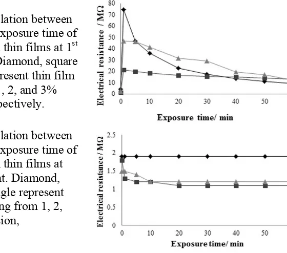
Electrical Resistance of ZnPcSn Thin Film with Ozone Exposure
The measured electrical resistance of ZnPcSn thin film under ozone exposure is shown
in Figure 5. This figure shows that long exposure time with ozone leads to the decreasing of electrical resistance. The interaction between ZnPcSn thin film and ozone molecule in this
research is proposed to occur as in Equation (1).
O3 + ZnPcSn ⎯adsorption⎯⎯⎯⎯→(O3 ads , ZnPcSn)
(O3 ads , ZnPcSn)⎯⎯⎯⎯⎯⎯→
transfer charge
O3- + ZnPcSn+
O3- + ZnPcSn+ ⎯delocaliza⎯⎯⎯⎯tion⎯→(O3- , ZnPcSn) + charge carrier (1)
The electrical resistance becomes lower at the increasing of ZnPcSn suspension
concentration from 1% to 2%. It seems that surface morphology of the thin film is strongly related to its electrical behaviour. However, ZnPcSn 3% suspension gave incomparable thin
film due to its roughness and discrete form. Furthermore, Equation (1) shows that the decreasing of electrical resistance is due to the increasing of released charge carrier.
Figure 5. Correlation between resistance and exposure time of various ZnPcSn thin films at 1st measurement. Diamond, square and triangle represent thin film resulting from 1, 2, and 3% suspension, respectively.
Figure 6. Correlation between resistance and exposure time of various ZnPcSn thin films at 2nd measurement. Diamond, square and triangle represent thin film resulting from 1, 2, and 3% suspension,
respectively.
Figure 5 shows the initial electrical resistance is low, after exposing by ozone at 0-1 min, the electrical resistance is increased. This may due to displacement of O2 molecule from
metal surface sites at partly of the thin film surface [17]. After exposing by ozone at 1-60 min, the electrical resistance would decrease because of the increasing of adsorbed ozone.
The electrical resistance of ZnPcSn thin film was measured again with ozone exposure
CONCLUSION
Based on this research and discussion, it can be concluded that the smoothness and continuity of ZnPcSn thin film is strongly related to the increasing concentration of ZnPcSn suspension, resulting in more amount of ozone can be adsorbed to the thin film. The amount of charge carrier will increase with the increasing of adsorbed ozone, so the thin film resistance will decrease. The thin film of ZnPcSn is suitable for ozone detector because its
resistance decreases irreversibly toward ozone exposure.
ACKNOWLEDGEMENT
The authors would like to thank to Biro Perencanaan dan Kerjasama Luar Negeri
(BPKLN), The Ministry of Education and Culture of Indonesia, for research funding through
the Fast Track Program.
REFERENCES
[1] B. Gunawan, Teknologi Sensor Kimia, MAWAS, Edition June, 2010, 1-9.
[2] J. Brunet, A. Pauly, L. Mazet, J.P. Germain, M. Bouvet, B. Malezieux, Thin Solid
Films, 2005,490, 28-35.
[3] A. Schütze, N. Pieper, J. Zacheja, Sens. Actuators B, 1995, 23, 215-217.
[4] M. Bouvet, G. Guillaud, A. Leroy, A. Maillard, S. Spirkovitch, F.G. Tournilhac, Sens.
Actuators B, 2000, 73, 63-70.
[5] A. Schütze, U. Weber, J. Zacheja, D. Kohl, W. Mokwa, M. Rospert, J. Werno, Sens.
Actuators A, 1993, 37-38, 751-755.
[6] S. Pochekailov, D. Rais, S. Nešpůrek, J. Rakušan, M. Karásková, Material
Science-Poland, 2009, 27, 781-795.
[7] G.K. Karaoğlan, G. Gümrükçü, A. Koca, A. Gül, U. Avciata, Dyes and Pigments, 2011, 90, 11-20.
[8] K. Han, K. Kay, Bull. Korean Chem. Soc., 2005, 26, 1274-1276.
[9] A. Ogunsipe, D. Maree , T. Nyokong, J. Mol. Struct., 2003, 650, 131-140.
[10] P.M. Matlaba, Synthesis of Zinc Phthalocyanine Derivatives for Possible Use in Photodynamic Therapy, Department of Chemistry, Rhodes University, Grahamstown, 2002.
[11] Nasikhudin, K. Triyana, National Conference of MIPA, State University of Malang, 2010.
[12] C.J. Kikkert, RF Electronics Chapter 10: Circuit Manufacture, http://www.ltcc.de/, March 21th 2013.
[13] G. Maggioni, A. Quaranta, S. Carturan, E. Negro, A. Patelli, M. Tonezzer, G.D. Mea,
Proceedings of the 16th International Symposium on Plasma Chemistry (ISPC-16),
Taormina, Italia, 2003.
[14] S.M. Critchley, M.R. Willis, M.J. Cook, J. McMurdo, Y. Maruyama, J. Mater. Chem., 1992, 2, 157-159.
[15] A. Siejak, D. Wrόbel, P. Siejak, B. Olejarz, R.M. Ion, Dye and Pigments, 2009, 83, 281-290.
[16] R.T. Tjahjanto, D.G. Ratnawati, S. Wardhani, J. Pure App. Chem. Res., 2012, 1(1), 18-25.