We also propose a more accurate view of the GaP interface between Zn3P2 and GaAs, based on the atomic structure, chemical bond, band diagram and P-displacement energy, than previously expected. We also investigate structures and energies of the transition states in the first hydrogen dissociation of a water molecule on the (2×4) surface.
Surfaces of III-V semiconductors
Studying the surfaces of GaAs and GaP is important because both materials suffer from degradation of electronic properties due to a high density of surface states.[9, 10] This is one of the major barriers to the widespread use of compound semiconductors in instead of Si, despite their superior optoelectronic properties. Second, the electronic properties of the semiconductor change due to the donation or depletion of electrons by the chemical adsorbates.
Major surface study tools used in this dissertation
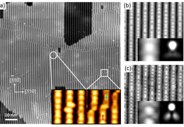
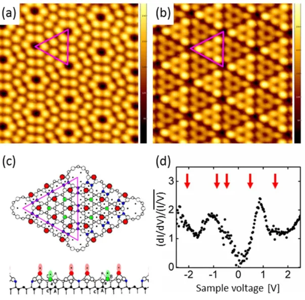
In the STM image obtained with a sample bias voltage of + 1.7 V in Figure 1.1a, there is no difference in the STM images of the two half-cells. The shift of the peak to the base level is due to the chemical environment of the element of interest.
Summary
We also describe a precise picture of the structural and electronic properties of the GaP interface between Zn3P2 and GaAs. We explored all reasonable ground states involved in most possible absorption and decomposition pathways using DFT simulations.
Introduction
In this chapter, we report the detailed chemical, structural, and electronic properties of the surface and interface of pseudomorphic Zn3P2 epilayers grown on the GaAs(001) surface. Line tunneling microscopy (STM) and high-resolution X-ray photoelectron spectroscopy (XPS) were used to elucidate the geometric and electronic structure of Zn3P2 films at the initial stages of growth under different conditions.
Experimental and computational details
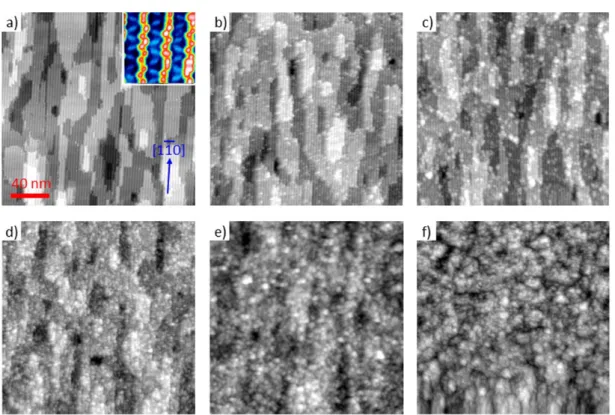
Zn3P2 epilayers were grown on the clean, well-defined (6x6) surface at normal growth temperature (180 ˚C) and different high temperatures (≥ 300 ˚C) using composite source MBE technique. The Zn3P2 flux was maintained by applying a constant power to the Zn3P2 loaded effusion cell, yielding an effusion cell temperature of 420 ˚C and a chamber background pressure of approximately 1 x 10⁻⁹ Torr. E(mnl) is the calculated total energy of the surface model at 0 K using the method described above.
Scanning tunneling microscopy
However, in most cases only one of the two locations is occupied by a Ga-As or As-As dimer. Most of the dimer sequences are composed of single peanut-shaped features in a (2×4) unit cell.
Scanning tunneling spectroscopy
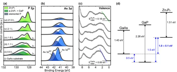
Exposure of the clean surface to the Zn3P2 flux resulted in significant changes in the observed tunneling spectra. The band gap is significantly different from the known crystalline Zn3P2 band gap of 1.5 eV [16, 28] Instead, the large band gap on this surface is close to the known GaP band gap of 2.26 eV. Finally, tunneling spectra obtained from Zn3P2/GaAs(001) grown at 180 ˚C (Figure 2.5d) showed an apparent band gap of 2.30 eV, which is again significantly larger than the band gap of Zn3P2.
The largest apparent band gap is attributed to the surface overlay phase composed of amorphous zinc phosphide (a-ZnPx) and elemental P.
![Figure 2.5 a) Tunneling current versus sample voltage (I-V) spectra obtained from clean GaAs(001)-(6×6) [black], 3.7 L Zn 3 P 2 /GaAs(001) at 490 ˚C [red], and 13 L Zn 3 P 2 /GaAs(001) at 180 ˚C [blue]](https://thumb-ap.123doks.com/thumbv2/123dok/10407109.0/34.892.175.725.331.772/figure-tunneling-current-versus-sample-voltage-spectra-obtained.webp)
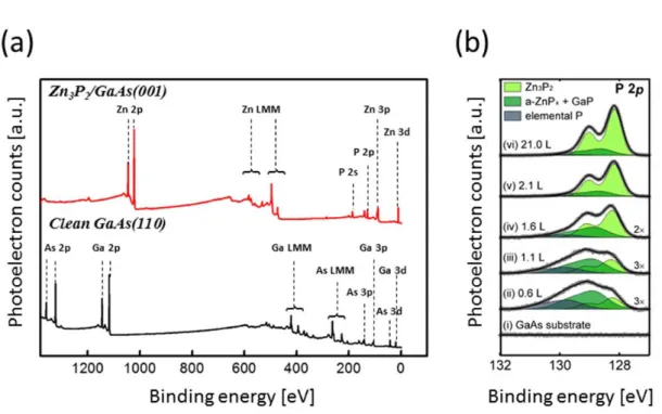
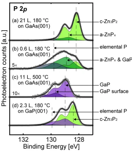
X-ray photoelectron spectroscopy
Therefore, tunnel spectroscopy supports the formation of the GaP layer on the surface of the GaAs(001) when exposed to Zn3P2 at high temperatures. To verify the binding energy shift of the GaP phase with respect to the c-Zn3P2. Thus, the existence of the GaP state for interfaces grown at high temperatures is supported by both internal and external evidence.
In addition, the binding energy shift of the GaP layer in Zn3P2/GaAs grown at high temperature is exactly matched by the known GaP binding energy.
Density functional theory calculations
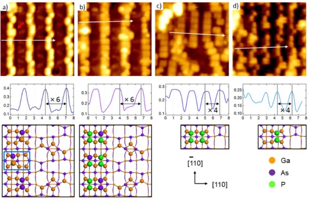
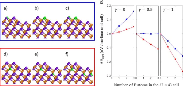
The result showed the formation of a Ga-P-Ga-P chain in the third layer at the plane intersecting the surface. First, at each chemical potential of As, the red points lie below the blue points, meaning that substitution of As for P in the subsurface region is energetically more favorable than that at the surface. On the other hand, substitution of surface As for P is exothermic when the chemical potential of As is sufficiently lower (e.g., γ ≤ 0.5).
Finally, anion substitution occurring at a site deeper than the third layer is energetically less favorable than that at the third layer.
Conclusion
Second, at the experimental conditions reported herein, for example at a low As chemical potential, which is assumed to be γ = 0.5 and 1, replacement of subsurface As by P is exothermic. Third, the anion substitution is initiated from the third layer that is below the surface As dimer block, followed by the second substitution in the fifth layer below the As-As dimer that is at the trough. DFT simulations explain that when appropriate activation energy is provided, the anion substitution of As by P in both surface and subsurface is exothermic under P rich and As poor conditions.
In addition, As atoms in the third layer are preferentially replaced by P atoms by forming the (Ga-P)n chain.

Introduction
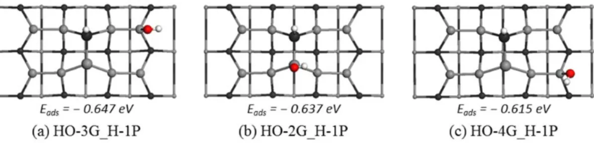
Despite the wealth of quantum mechanical studies on adsorption, dissociation or decomposition reactions of water on the (001) surfaces of elemental semiconductors such as silicon and germanium [67-70], there are few studies on any surface of III-V zinc blends. semiconductors such as GaAs, GaP and InP [66]. Moreover, little molecular-level information has been reported on the adsorption and degradation mechanisms of water on the GaP(001) surface. In this paper, we report DFT studies on the adsorption and degradation of a water molecule on the GaP(001)(2 4) surface.
This provides the fundamental thermodynamics for the initial adsorption and dissolution processes of water molecules on the GaP(001)(2 4) surface.
Computational details
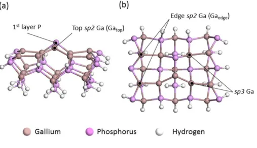
Two likely Ga-rich reconstruction structures have been suggested from previous theoretical studies Ga-P mixed dimer surface reconstruction and (2 4) Ga-Ga dimer surface reconstruction. However, experimental studies argued that the mixed Ga-P dimer was more stable than the Ga-Ga dimer under the commonly achievable Ga-rich conditions. Thus, we chose the Ga-rich GaP(001)(2 4) mixed dimer surface reconstruction structure as the clean surface structure in this study.
A mixed GaP(001)(2 4) dimeric Ga-rich surface was modeled using a periodic slab geometry consisting of six Ga and P layers with a vacuum region equivalent to ten Ga and P layers (Figure 1.3b).
Result and discussion
P buckling**
That is, when the second hydrogen atom is bonded to the Ga atom that is a member of a Ga-O-Ga bridge configuration, the adsorption energy is the least among the five structures. This is because the Ga-O-Ga configuration leads to the best energy of the O/2H ground states. For example, the black lines along the reaction coordinates indicate the ground states in the dissolution mechanism of the water molecule adsorbed at the 2G site.
However, since we have not verified the transport mechanism of the second hydrogen atom from the HO configuration to the H-Ga configuration, we cannot conclude which pathway is preferred.
Conclusion
The molecular adsorption state of water, where we find that the molecular adsorption geometry is most stable when H2O is adsorbed on top of the surface sp2 Ga atom of either the mixed Ga-P dimer or the Ga-Ga dimers. The HO/H decay state, where we find that the HO group bonds to a surface sp2 Ga atom and the H bonds to the P atom of the first shell, where both the HO and H groups have the top configurations. The O/2H decomposition state, where the thermodynamically favorable adsorption structure for the O atom is the bridged Ga-O-Ga structure.
The surface oxide state, where the O atom forms the Ga-O-Ga bridging oxide configuration after desorption of H2.
Introduction
Covalent bonding between S and III-V semiconductor surface atoms can be used to graft molecules onto the surface.[98] This strong grafting is necessary in the modification and functionalization of the semiconductor surface with organic molecules. Despite its importance, fundamental research on adsorbate structures and related energetics on III-V semiconductor surfaces has not yet been fully performed. In addition, most surface studies of alkanethiol molecules adsorbed on III-V semiconductors have been dependent on spectroscopic techniques such as X-ray photoelectron spectroscopy (XPS) and thermal desorption spectroscopy (TDS).
We also investigate the effect of annealing on adsorption geometry and binding characteristics using X-ray photoelectron spectroscopy (XPS) and the previous two techniques.
Experimental and computational details
In Equation (4.1), Iov and Isub denote integrated peak areas of the element of interest in the overlay and substrate, respectively. The escape depths of photoelectrons through the molecular overlays were approximated by an attenuation length (λ) calculated using the following empirical equation where E is the kinetic energy of the photoelectron in eV and a is the diameter of the atoms in is the monolayer in nm. . The escape depths of the S 2p and C 1s photoelectrons through the 1-propanethiol overlay were calculated to be 2.551 and 1.841 nm, respectively.
The adsorption energy (Eads) of a molecule of interest adsorbed on the GaP(001)(2×4) surface was calculated by subtracting the sum of the energies of the molecule and the bare GaP(001)(2×4) cluster from the cluster energy GaP adsorbed by molecules,.
Results and discussion
The STM image of the aggregated feature differs from the aggregated molecules in Figure 4.3b as it can The adsorption location of feature B is similar to that of feature A' in Figure 4.4b. At higher temperatures, we saw two features from the STM images; an intense bump at the centerline of the (2 × 4) unit cell (feature C) and a less intense bump near the edge of the sp2 Ga atom (feature D), as shown in Figure 4.4d.
Kimball, G.M., et al., Photoluminescence-based measurements of the energy gap and diffusion length of Zn3P2. Jenichen, A., et al., Nitrogen substitutions in GaAs(001) surfaces: density functional supercell calculations of surface stability. Moriarty, P., et al., Photoelectron nuclear spectroscopy and scanning tunneling microscopy study of the sulfur-treated Gaas(100) surface.