Introduction
Research motivation
Therefore, wearable devices should measure appropriate biosignals or activity indicators depending on the user's purpose. As a result, a wearable device that supports PTT-based blood pressure estimation needs to measure appropriate biosignals such as ECG and PPG, and needs low-power performance for long-term use.
Thesis organization
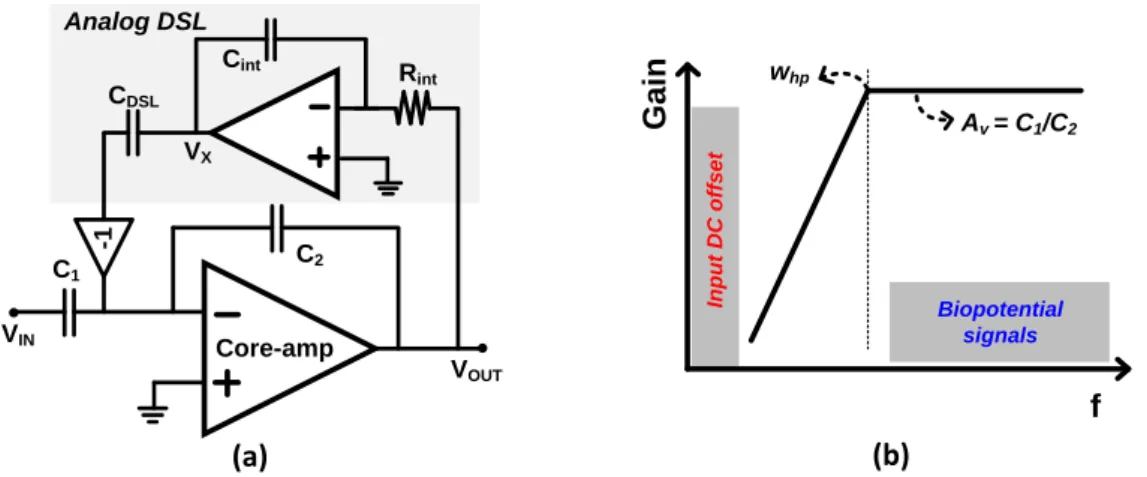
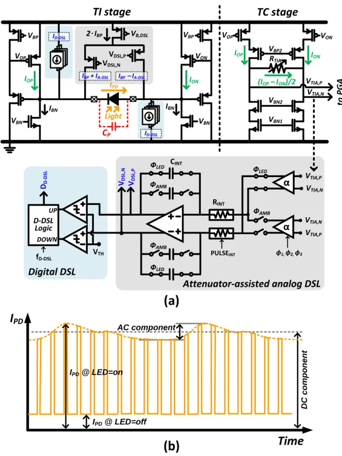
From equation (4.1), the passband gain (AV) and the HPF cutoff frequency (whp) are CCIA. The differential outputs of the TIA (VTIA,P, VTIA,N) are fed to a switched-capacitor programmable gain amplifier (PGA).
Backgrounds for continuous blood pressure monitoring
Healthcare system interface for continuous BP monitoring
They are then transferred to the controller and application equipment for additional digital processing and control of the monitoring system. Therefore, this research focused on the biopotential and optical-based signal circuit design with various proposed design techniques and architectures to minimize the digital signal processing and power consumption of the sensor module.
Electrocardiogram
- Basic of electrocardiogram
- Requirements for biopotential signal acquisition
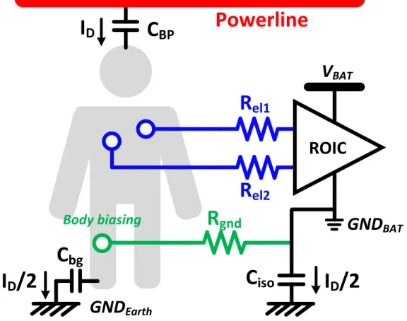
If the impedances of both input electrodes are zero, power line interference is observed at the output by multiplying the common-mode gain of the amplifier (ACM). Since the biopotential signal is applied as differential input to both electrodes, it is sensed at the output by multiplying the differential gain of the amplifier (ADM).
Photoplethysmogram
- Basic of photoplethysmogram
- Requirements for PPG signal acquisition
Some part of the photodiode current needs to be analyzed to design an optimized PPG readout circuit. Finally, the LED's power consumption must be reduced to implement a low-power system design.

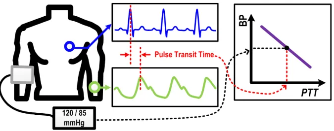
Blood pressure estimation using pulse transit time
- Non-invasive BP estimation methods
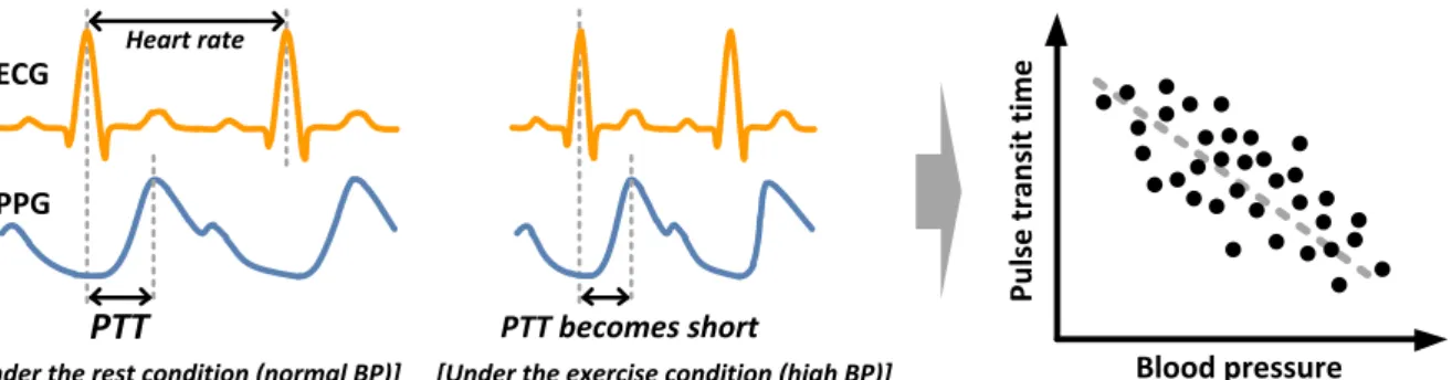
- Relation between pulse transit time and blood pressure
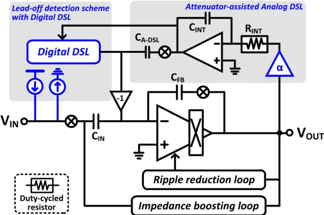
It is determined by the maximum swing range of the DSL integrator output (VDSL, MAX), the analog DSL feedback capacitor (CA-DSL), and the input capacitor (CIN). Digital DSL logic enhances the output of digital DSL (DD-DSL), where the logic operation is synchronized by the digital DSL clock (fD-DSL).
Technical backgrounds for biopotential and PPG signal acquisition
Technical backgrounds for biopotential signal acquisition
- Relationship between amplifier gain and ADC resolution
- Lead-off detection in biopotential signal sensing
- DC-servo loop for input DC offset cancellation
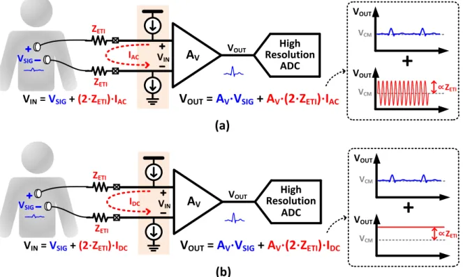
AC lead detection sends AC current (IAC) through the input terminals of biopotential AFE through the electrode-tissue impedance (2·ZETI). The DC discharge detection sends DC current (IDC) through the input terminals of biopotential AFE through the electrode-tissue impedance (2·ZETI).
Technical backgrounds for PPG signal acquisition
- System architecture for PPG sensing in other works
- Photodiode junction capacitance
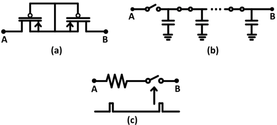
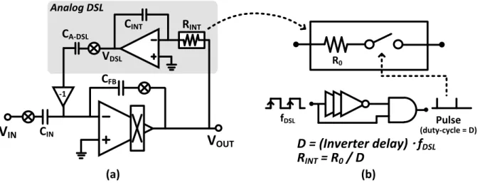
The transfer function of LNA with the proposed analog DSL using attenuator is expressed as follows. As shown in Figure 4.7, the operation of the attenuator is synchronized with the switching of the cyclic resistor (PULSEINT) in the DSL integrator. The performance characteristics of the PGA can be analyzed from the circuit diagram in Figure 4.13(a), and each equivalent resistor (RIN, RFB, ROS) is expressed as each capacitor (CIN, CFB, COS) and the switching frequency (fCLK).
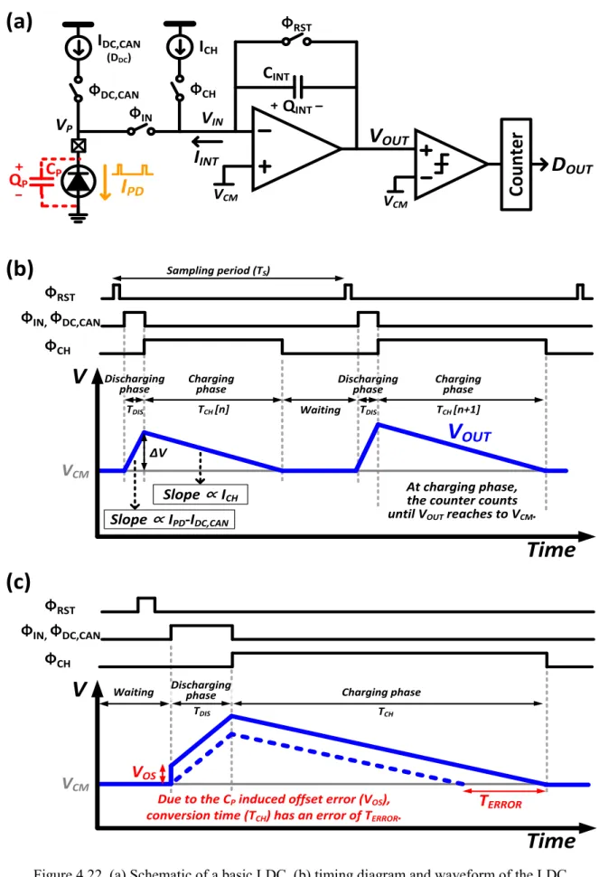
However, since the junction capacitance of the photodiode (CP) exists, it does not work ideally as shown in figure 4.22(b). The input photodiode current is measured from the obtained outputs of the DDC and DOUT.
Implementation of multi-physiological sensing ROIC
ROIC architecture
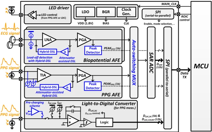
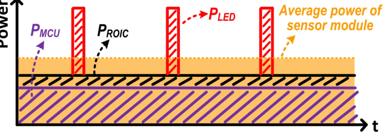
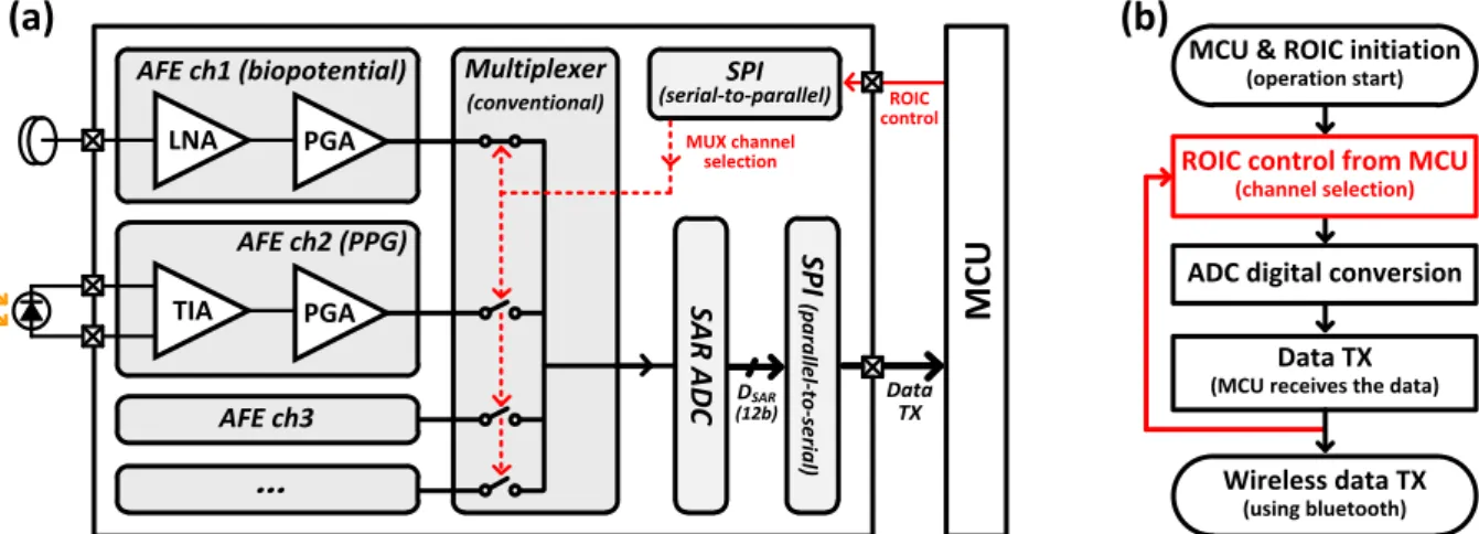
To support this, a readout-optimized integrated circuit (ROIC) is designed, and Figure 4.1 shows the architecture of the proposed ROIC, which includes biopotential analog input terminals, PPG AFE analog input, light-to-digital converter, successive approximation register ADC, and various circuits for system integration. As mentioned in Section 2.1, the total power consumption of the input link, ROIC and controller should be lowered to reduce the power consumption of the sensor module. In particular, the power of the LED for PPG measurement and the power of the MCU for the overall operation of the system take a significant proportion of the energy consumption.
Because the PPG AFE takes a long settling time on the output voltage due to the junction capacitor of the photodiode and the required LED turn-on time is proportional to the settling time, the LED power consumption is significant. The proposed auto-switching multiplexer replaces a role of the MCU for channel switching for a multi-channel signal acquisition, so that the low-performance MCU can be operated with reduced power consumption.
Implementation of biopotential analog front-end
- Low-noise amplifier
- Analysis of the conventional LNA
- Proposed attenuator-assisted analog DC-servo loop
- Proposed lead-off detection scheme with digital DC-servo loop
- Programmable-gain amplifier
Vni, CORE and Vni,DSL are input-referenced noises from the core amplifier and the DSL amplifier, respectively. The input-referenced noise of the LNA, which is caused by the Vni, kernel and Vni.DSL, is expressed in equations (4.5) and (4.6). Schematic CCIA for (a) noise analysis and (b) offset analysis of the core amplifier and the DSL amplifier.
An attenuator circuit added to the input of the DSL analog path attenuates the output of the LNA by an attenuation coefficient (α) and delivers it to the input of the integrator. Determines how much the input signal is attenuated and transferred to the analog DSL input.
Implementation of PPG analog front-end
When Kirchhoff's current law is applied to the cathode and anode of the photodiode in Fig. 4.17(a), we obtain the following equations. And then the third term in equation (4.24) is equal to the AC component of the photodiode current (IPD,AC) and is shown in the differential outputs of the TIA (VTIA,P, VTIA,N) without the output offset. The transconductance gm is the return current of the analog DSL to remove the DC current flow of the photodiode and can be seen as a pair of PMOSs, each connected to a photodiode in the TI stage of Fig. 4.17(a).
Therefore, as shown in the figure 4.16, a timing logic is designed so that the whole components of the PPG AFE work in synchronization and the figure 4.19(a) shows the timing diagram and output waveforms of the TIA and PGA. The capacitance makes it take a long time for the voltage across the photodiode to drop at the moment the LED is turned on, which is also related to the drop of the TIA output voltage.
Light-to-digital converter with proposed pre-charging scheme
The term IPD - IDC,CAN is called the photodiode current residual current (IRES). ICH, which is the charge current of the integrator, flows until VOUT becomes VCM. Since DDC and DOUT are transferred as the output of the LDC, the input current of the photodiode can be found using equation (4.32).
The charge stored in the capacitor of the integrator (QINT) and the charge stored in the junction capacitance are expressed by the following equations. As the IAMB discharges the integrator, the output of the integrator (VOUT) increases in proportion to the IAMB, and the VOUT voltage has a VCM.
Analog peak detector
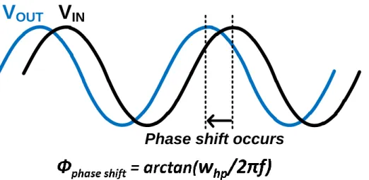
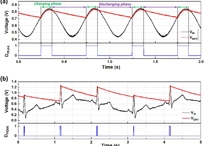
VENV should be lowered very slowly so that the peak (DPEAK) is detected accurately near the next peak. The generated VENV voltage is compared with VIN through a hysteresis comparator which is implemented to resist an instability due to the noisy signal condition in the VIN and as a result the peak is usually extracted near the peak. Measured waveform of the analog peak detector with (a) steady sinusoidal input and (b) ECG waveform with baseline wandering artifact.
In the discharge phase of the peak detector operation, the peak value (DPEAK) is emitted from a point slightly lower than the actual peak point of the input signal (VIN) because the envelope waveform (VENV) continuously drops from a voltage from the previous peak position and is compared to the VIN at the next peak position. Therefore, although the analog peak detector has the advantage of being able to detect the peak inside the chip, it is difficult to detect the exact peak position.
Multi-channel analog-to-digital conversion
- Successive approximation register ADC
- Proposed multiplexer with auto-switching scheme
The input sampling phase of the SAR-ADC must also be considered to implement a multi-channel signal acquisition with a signal ADC, which will be described in chapter 4.6.2. A basic structure of the ROIC for multi-channel signal acquisition is to connect one ADC for each analog front-end [34]. The MCU closes the multiplexer switch of the channel to be digitally converted by applying the ROIC control signal.
After the MCU receives the output data, the ROIC control signal is applied again for the digital conversion of the next channel, and another channel is selected to perform the digital conversion and data transmission to the MCU repeatedly. Therefore, the conventional ROIC structure requires a high MCU operation, which increases the power consumption of the MCU. a) Conventional ROIC structure for multi-channel signal acquisition using a single ADC and (b) its operation flow chart.
Experimental results of the ROIC
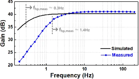
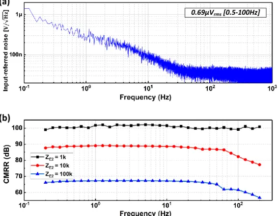
- Experimental results of the biopotential AFE
- Experimental results of the PPG AFE and LDC
- Minimized MCU power consumption
- Summary
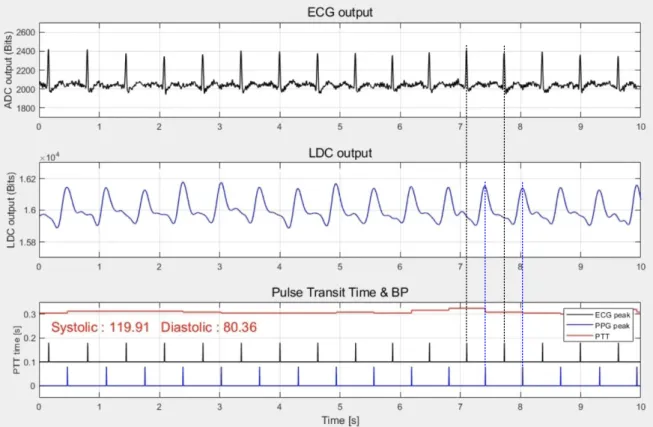
The accuracy of BP estimation based on pulse transit time was compared for 4 subjects using two measurement systems in each. Operation of a real-time continuous blood pressure monitoring system on (a) a smartphone and (b) a Matlab interface on a PC. Compared to each result of the four subjects in Figure 5.3, the results in Figure 5.8 obtained using a PC-based continuous blood pressure monitoring system show similar trends.
Real-time operation of the continuous blood pressure monitoring system with significant digital signal processing in PC Matlab interface. To ensure long-term use of the blood pressure monitoring system, the power consumption of the entire sensor module must be kept to a minimum.
Implementation of continuous blood pressure monitoring systems
Portable continuous BP monitoring system with minimized DSP
- System architecture
- Experimental results
PPG waveforms are digitally converted using the auto-switching multiplexer and a SAR-ADC (DSAR), then the ECG and PPG outputs and their peaks are transmitted to the MCU. Relationship between the measured systolic blood pressure and pulse transit time by the portable BP monitoring system for four subjects. Relationship between the measured SBP and estimated SBP, and their Bland-Altman plots for four subjects using the portable BP monitoring system.
Relationship between measured SBP and estimated SBP and their Bland-Altman plots for the four PTT-BP equations using a portable BP monitoring system. From the overall results in Figure 5.5, it is confirmed that all the results using the four PTT-BP equations had quite similar correlation coefficients and standard deviations.

Stationary continuous BP monitoring system
- System architecture
- Experimental results
Blood pressure is estimated from a pulse transit time that is the time difference of the ECG and PPG, and therefore the simultaneous measurement of ECG and PPG, the detection of their peaks, and the calculation of the pulse transit time must be performed in real time. The MCU occupies a significant amount of power consumption of the developed sensor module, excluding the Bluetooth module for wireless communication. The proposed auto-switching multiplexer replaces a role of the MCU for channel switching for a multi-channel signal acquisition, and the analog peak detector detects ECG and PPG peaks directly from the biopotential and PPG AFE output voltage.
Carvalho, “Is pulse transit time a good indicator of blood pressure changes during brief exercise in a young population?” In Proceedings of the 2010 IEEE Engineering in Medicine and Biology (EMBC) Annual International Conference, Buenos Aires, Argentina, August 31–4. September 2010; p. Zhang, “Cuffless and noninvasive measurement of arterial blood pressure with pulse transit time,” In Proceedings of the 27th Annual International Conference of the Engineering in Medicine and Biology Society (EMBS 2005), Shanghai, China, 1–4. September 2005;.
Conclusion