i
WIDEBAND SPDT SWITCH FOR RF APPLICATIONS
AURTHER CHOW ZHA KHANG
This report is submitted partial fulfillment of the requirement for the award of Bachelor
of Electronic Engineering (Industrial Electronics/ Telecommunication Electronics/
Computer Engineering/ Wireless Communication) With Honours
Faculty of Electronic and Computer Engineering
Universiti Teknikal Malaysia Melaka (UTEM)
ii
UNIVERSTI TEKNIKAL MALAYSIA MELAKA
FAKULTI KEJURUTERAAN ELEKTRONIK DAN KEJURUTERAAN KOMPUTER
BORANG PENGESAHAN STATUS LAPORAN
mengaku membenarkan Laporan Projek Sarjana Muda ini disimpan di Perpustakaan dengan syarat- syarat kegunaan seperti berikut:
1. Laporan adalah hakmilik Universiti Teknikal Malaysia Melaka.
2. Perpustakaan dibenarkan membuat salinan untuk tujuan pengajian sahaja.
3. Perpustakaan dibenarkan membuat salinan laporan ini sebagai bahan pertukaran antara institusi
pengajian tinggi.
4. Sila tandakan ( √ ) :
SULIT*
TERHAD*
√ TIDAK TERHAD
(Mengandungi maklumat yang berdarjah keselamatan atau kepentingan Malaysia seperti yang termaktub di dalam AKTA RAHSIA RASMI 1972)
(Mengandungi maklumat terhad yang telah ditentukan oleh organisasi/badan di mana penyelidikan dijalankan)
Disahkan oleh:
(COP DAN TANDATANGAN PENYELIA)
iii
3
“I hereby declare that this report is the result of my own work except for quotes as cited in the
references.”
Signature :
Author : AURTHER CHOW ZHA KHANG
iv
4
“I hereby declare that I have read this report in my opinion this report is sufficient in terms of the
scope and quality for the award of Bachelor of Electronic Engineering
(Wireless Communication) with Honors.”
Signature :
Supervisor Name : Mr. NOOR AZWAN BIN SHAIRI
v
5
Especially for
To beloved parents,
My brother & sister
My supervisor
Mr. Noor Azwan Bin Shairi
And all my friends
vi
6
ACKNOWLEDGEMENT
First of all, I would like to thanks to my beloved family who’s given their warm support
and trust on me throughout my time at university. Their unflinching courage and conviction will
always inspire me, and I hope to share my achievement in university with them. Without their
love and care, it is impossible for me to complete this degree program in UTeM.
I also would like to send my sincere respect to my supervisor; Mr. Azwan B. Shairi. He
always helps me in this project by providing his wide knowledge in this field. Besides that, he
also gives different kind of support to help me during this project duration. I am appreciating
what he had done for me and hopefully blessing will with him in the rest of his life.
Finally I would like to express appreciation to all my friends and others people who have
helped me directly or indirectly with their knowledge, moral support and encouragement on me.
This project is not my effort only but is the result of all people that helping me in this project. I
hope can express my appreciation through a sincere thank you from the deep of my heart at here.
vii
ABSTRACT
This project is discussed wideband RF switches for radio frequency (RF) applications.
The aim of this project is to increase the bandwidth of the switch as much as possible to be used
in various applications. This project is focusing on switch design by using PIN Diode. Besides,
this project will use Single Pole Double Throw (SPDT) switch type of the RF switch due to Time
Division Duplex which is transmit and receive shared the same frequency. This project is
focusing more on the topologies of the SPDT switch in improving bandwidth rather than use
different material. This project also discussed each topologies functionality, advantages and
disadvantages. The selected topologies are simulated by using Advanced Design Systems (ADS)
software. In the simulation result, we will discuss on the insertion loss and isolation of the switch.
In order to fabricate the switch in future, our requirement of insertion loss is less than 1 dB and
isolation is around 20dB. Modification will be made in topologies in order to maintain its
wideband characteristic and improve its insertion loss and isolation. 3 topologies are discussed in
this project which is 2 types of series-shunt-shunt topologies and Broadband shunt SPDT switch
topology. Tuning of each element in topologies is done by obtaining the best result in simulation
section. The best topology is selected as the topology that used in this project and fabrication is
carried out on to it by using FR-4 substrate board. Prototypes are measured and comparison
viii
ABSTRAK
Projek ini membincangkan suis RF yang berjalur lebar untuk kegunaan frekuensi radio.
Projek ini adalah bagi meningkatkan lebar jalur suis sebanyak yang mungkin untuk diguna
pakai dalam pelbagai kegunaan. Projek ini menumpukan atas reka bentuk suis dengan
menggunakan PIN Diode. Selain itu, projek ini akan menggunakan suis yang berjenis SPDT
disebabkan Time Division Duplex dimana menghantar dan menerima berkongsi frekuensi sama.
Dalam projek ini akan berfokus lebih mengenai topologi suis dalam meningkatkan lebar jalur
daripada gunakan bahan yang berlainan. Projek ini juga membincangkan setiap kefungsian
topologi, kelebihan dan keburukannya. Topologi yang dipilih akan disimulasi dalam ADS
(Advanced Design System). Dalam hasil dimulasi, kami akan membincangkan pada kehilangan
sisipan dan kuasa pengasingan suis. Keperluan kita untuk mencapai dalan penghilangan sisipan
adalah tidak kurang daripada 1dB dan kuasa pengasingan ialah 20dB supaya untuk mereka suis
pada masa depan. Pengubahsuaian dalam topology akan dibuat supaya mengekalkan jalur
lebarnya dan menurunkan penghilangan sisipan dan meningkatkan kuasa pengasingan. Tiga
topologi akan dibincangkan dalam projek ini dimana dua daripadanya ialah jenis series shunt
shunt topologi dan satu daripadanya ialah shunt SPDT suis yang berjalur lebar. Penukaran nilai-
nilai dalam topologi adalah untuk mendapatkan keputusan yang terbaik dalam seksyen simulasi.
Topologi terbaik dipilih sebagai topologi yang menggunakan dalam projek dan pembikinan ini
dijalankan dengan menggunakan papan substrat FR4. Prototaip akan diukur dan perbandingan
antara prototaip akan dibuat untuk memilih prototaip yang memiliki persembahan yang terbaik
x
2.1.1 Switch Parameter Definitions 8
2.1.1.1 Insertion Loss 8
3.1 Methodology Introduction 13
3.1.1 Project Flow Chart 14
3.2 Advanced Design System (ADS) 16
3.3 Schematic Design 16
3.4 Layout Design 19
3.4.1 Converting ideal component to reality component 20
3.4.1.1 Calculation for value capacitors and inductors 20
3.4.1.2 Adding in Transmission Line 21
xi
3.6.1 Electronic Calibration 26
4 RESULT AND DISCUSSION 27
4.1 Simulation result of first topology 27
4.2 Simulation result of second topology 35
4.3 Simulation result of third topology 42
4.3.1 Improvement of Topology 47
4.4 Simulation of Layout Design 53
4.5 Measurement of Prototype 59
4.6 Component List of Prototype 69
4.7 Comparison Between Two Prototypes 71
5 CONCLUSION 72
5.1 Conclusion 72
5.2 Recommendation 73
xii
13
LIST OF FIGURES
FIGURE TITLE PAGE
1.1 Single Series PIN diode switch schematic diagram 2
1.2 Return Loss of Single Series PIN diode switch 3
1.3 Isolation of Single Series PIN diode switch 3
1.4 Insertion Loss of Single Series PIN diode switch 4
2.1 Example of SPDT switch in Transceiver Block Diagram 8
2.2 Hierarchy of PIN diode HSMP-389Y 11
3.1 Methodology Flow Chart 15
3.2 Series-shunt-shunt topology with 2 dc biasing method 17
3.3 Series-shunt-shunt topology with 3 DC biasing method 18
3.4 Broadband shunt SPDT switch topology 18
3.5 Layout Design in Schematic Diagram 19
3.12 Example of Network Analyzer Calibrator 26
4.1 Schematic Diagram of First Topology 29
4.2 Return Loss S11, S22 & S33 30
4.3 Isolation Between Transmit and Receive 30
xiii
14
4.5 Isolation of Receive Mode 31
4.6 Return Loss S11, S22 & S33 32
4.7 Isolation Between Transmit and Receive 32
4.8 Insertion Loss 33
4.9 Isolation of Transmit Mode 33
4.10 Schematic Diagram of Second Topology 36
4.11 Return Loss S11, S22 & S33 37
4.12 Isolation Between Transmit and Receive 37
4.13 Insertion Loss 38
4.14 Isolation of Receive Mode 38
4.15 Return Loss S11, S22 & S33 39
4.16 Isolation Between Transmit and Receive 39
4.17 Insertion Loss 40
4.18 Isolation of Transmit Mode 40
4.19 Schematic Diagram of Third Topology 42
4.20 Return Loss S11, S22 & S33 43
4.21 Isolation Between Transmit and Receive 43
4.22 Insertion Loss 44
4.23 Isolation of Receive Mode 44
4.24 Return Loss S11, S22 & S33 45
4.25 Isolation Between Transmit and Receive 45
4.26 Insertion Loss 46
4.27 Isolation of Transmit Mode 46
4.28 Schematic Diagram of Improved Topology 47
4.29 Return Loss S11, S22 & S33 48
4.30 Isolation Between Transmit and Receive 48
4.31 Insertion Loss 49
4.32 Isolation of Receive Mode 49
4.33 Return Loss S11, S22 & S33 50
4.34 Isolation Between Transmit and Receive 50
xv
16
LIST OF TABLES
TABLE TITLE PAGE
4.1 Simulation Result of First Topology 34
4.2 Simulation Result of Second Topology 41
4.3 Simulation Result of Third Topology 47
4.4 Simulation Result of Improved Topology 52
4.5 Simulation of Layout Design 59
4.6 Comparison of simulation result and measurement result of prototype 1 64
4.7 Comparison of simulation result and measurement result of prototype 2 69
4.8 Component List 70
xvi
LIST OF ABBREVIATIONS
SPDT -Single Pole Double Throw
SPST -Single Pole Single Throw
RF -Radio Frequency
IL -Insertion Loss
TDD -Time Division Duplex
WiMAX -Worldwide Interoperability for Microwave Access
LTE -Long Term Evolution
WiBro -Wireless Broadband
TD_SCDMA -Time Division Synchronous Code Division Multiple Access
1
CHAPTER 1
INTRODUCTION
1.1. Introduction of Project
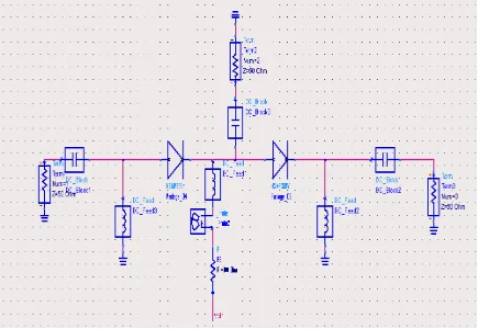
This project called “Wideband SPDT Switch for RF Application” which is a switch
that can operate in wide frequency range. SPDT stand for Single Pole Double Throw
meaning there are total number of 3 ports. 1 port is for antenna and the other 2 ports are for
transmitter and receiver. When the antenna is used to transmit signal, the receiver port will
isolated from antenna and vice versa. PIN diode HSMP-389Y from Avago Technologies is
used in the design for all the topologies. SPDT switch design is focus on the base station
2
1.2. Project Objectives
The objectives of this project are to study different switch topologies and analysis the
topologies to be a wideband switch. The best topology will be selected and fabricated by
using FR-4 substrate board and measure by using network analyzer.
1.3. Problem Statement
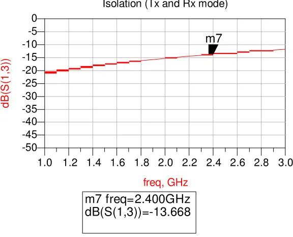
The HSMP-389Y PIN diode is a low performance PIN diode which cannot provide a
wideband properties without implement any topologies on it. The single series PIN diode
performance as a switch will be discussed and shown below.
3
Figure 1.2 Return Loss of Single Series PIN diode switch
0
4
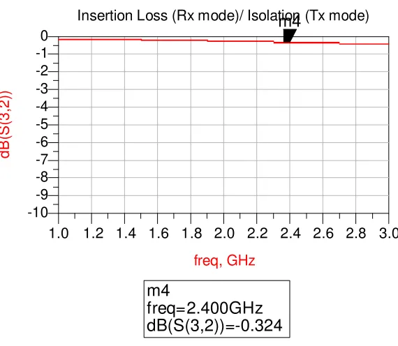
Insertion Loss (Rx mode)/ Isolatmio4n (Tx mode)
1.2 1.4 1.6 1.8 2.0 2.2 2.4 2.6 2.8
Figure 1.4 Insertion Loss of Single Series PIN diode switch
From the results of single series PIN diode switch, the isolation is only -13dB at
frequency 2.4GHz and drop when it going to high frequency. Therefore topology that used
in design should provide at least -20dB isolation at any operation frequency range which is
only 0.01% signal leakage.
1.4. Project Scopes
The scopes of this project are mainly focus on the switch topologies. Besides that, the
characteristic of PIN diode as a switch will also affect the bandwidth of the switch. Based on
literature review, those factors will be in count in designing stage. Below are the project
5
i. Understanding the basic knowledge of RF switch for WiMAX application.
Understand the differences of DC signal and RF signal in a SPDT switch.
The flow of these signals will help in determined the values of component
and connection of the circuit.
ii. Understanding the characteristic of PIN diode as a switch
In wideband SPDT switch, there are different component can be act as a
switch like Bipolar Junction Transistor (BJT), MESFET, PIN diode and
others. The advantages of a PIN diode to be place in this project will be
discussed in literature review section.
iii. Determine the suitable topology of SPDT switch for wideband purpose.
Since this project aim is to design a wideband SPDT switch, so the best
topology will be refer as a topology which give widest range of frequency
and acceptable isolation, insertion loss and return loss.
iv. Analyze and improve the selected switch topologies by using ADS software.
From the selected topologies, improvement will be made on it to obtain the
target result in this project. Some topologies might not be the best before
modification made but might give the best result after improvement done on
6
v. RF switch layout in ADS software.
After simulation, the obtained best topology is in schematic diagram and
cannot to be used for fabrication. The layout of the switch need to be draw
out in ADS software for fabrication purpose.
vi. Fabricate the layout on FR-4 substrate board.
Fabricate the layout draw in ADS software on a FR-4 substrate board.
Soldering of each element in schematic diagram is needed in order to
complete the prototype.
vii. Test the prototype Scattering Parameter by using network analyzer.
The best topology result in simulation is compared with the measurement
result. Analysis will be carrying out on the comparison and discussion and
comment will be making on it. S-parameter is use in this project due to its
easy implementation on a 3 port network
.
1.5. Structure of the Report
In this report will cover the objectives, background, simulation, measurement,
results a n d c o n c l u s i o n of this project. Discussion of the circuit design is included in
7
CHAPTER 2
LITERATURE REVIEW
2.1 RF Switch
RF switch is commonly used in RF transceiver system to perform Time Division
Duplex switching for transmit and receive operation. In microwave systems, the transceiver
requires several switches which are low-power switches and high power switches. Low
power switches are used in phase shifters and attenuators while high power switches is
normally used in radar application and communication systems. Besides that, the switches
can also be categorized into 2 categories which are reflective and non-reflective. Reflective
switches are switches that are closed between ports In and Out 1, port Out 2 is not connected
or it is open and any signal appearing at this port will be reflected. Non-reflective switches
are not suitable in many applications due to the introduction of significant standing wave
between the components. Switches having the unused port terminated in 50 ohm are non-