i
“I hereby declare that I have read this report and in my opinion this report is sufficient in term of the scope and quality for the award of Bachelor of
Electrical Engineering (Power Electronic and Drive) With Honours”
Signature : ………
Supervisor : Mr. Loi Wei Sen
ii
COMBINE INFRARED LOCK-IN THERMOGRAPHY AND CURVE TRACER INTO AN INTEGRATED SYSTEM
PHUNG LEE MUN
A report submitted in partial fulfillment of the requirements for the degree of Electrical Engineering (Power Electronic and Drive)
Faculty of Electrical Engineering
UNIVERSITI TEKNIKAL MALAYSIA MELAKA
iii
“I hereby declare that this report is result of my own effort except for works that have been cited clearly in the references.”
Signature : ………..
Author : Phung Lee Mun
iv
DEDICATION
To my beloved God, family, supervisor (Mr. Loi Wei Sen), co-supervisor (Mr. Ng
Kiong Kay), and my friends for giving assistant to complete this final year project
v
ACKNOWLEDGEMENT
Taking this opportunity, I would like to express my gratitude to Universiti Teknikal
Malaysia Melaka (UTeM) for offer this final year project (PSM) to all its last year students.
I would also like to thank Infineon Technologies (Malaysia) Sdn Bhd for giving me this
great opportunity to proceeds company project as my PSM with the greatest exposure
towards semiconductor industry. I am utmost grateful and delight to receive this project
offer from such a prestigious and worldwide company.
First and foremost, I would like to thank my respective supervisor, Mr Loi Wei Sen
for giving me an opportunity to carry out my PSM under his supervision. I would also like
to thank my respective co-supervisor, Mr. Ng Kiong Kay for his guidance and support for
the project during my attachment in the company. His advices shall be a guide to me in my
future undertakings. I am deeply thankful for his kindness and willingness in teaching me
to handle variety of machines and explained theories and operations of processes involved
in the semiconductor industry.
Last but not least, a big thank you to my dearest family for having being there for
me. Without them, my PSM will not turn out to be so great. And I strongly believe that all
the precious experience that I gained during the 2 semester of PSM will make me become a
vi
ABSTRACT
Both machines curve tracer and Infrared Lock-in Thermography (IR-LIT) are for
troubleshooting failure semiconductor devices. IR-LIT is basically based on the application
of a periodic input energy wave, which provides infrared and heat to the surface of the
object being examined. By this, IR-LIT localize and detects failure parts in a discrete
semiconductor device. A curve tracer is a piece of electronic test equipment used to
analyse the characteristics of semiconductor devices such as reverse leakage current and
reverse breakdown voltage. Based on an oscilloscope, the device contains current and
voltage sources that can be used to stimulate the device under test(DUT). It works by
applying a swept voltage to the terminals of the DUTs, and it measures too the amount of
current that the device permits to flow at each voltage. The V-I (voltage versus current)
graph or curve is displayed on an oscilloscope screen. However, failure devices can only be
examined separately using both machines for troubleshooting. The purpose of this project
is to build a hardware comprising of resistors, capacitors and MOSFET to combine the
usage of both machines together, in order to get the waveform from the curve tracer and
vii
ABSTRAK
Kedua-dua mesin curve tracer dan Infrared Lock-in Thermography (IR-LIT) adalah untuk
menyelesaikan masalah kegagalan peranti semikonduktor. IR-LIT pada asasnya
berdasarkan aplikasi input berkala gelombang tenaga, yang menyediakan inframerah dan
haba ke permukaan objek yang diperiksa. Dengan ini, IR-LIT memeriksa lokasi dan
mengesan bahagian kegagalan dalam peranti semikonduktor diskret. Curve tracer
merupakan sebuah peralatan ujian elektronik yang digunakan untuk menganalisis ciri-ciri
peranti semikonduktor seperti kebocoran arus dan pecahan voltan. Berdasarkan osiloskop,
peralatan ini mengandungi arus dan sumber voltan yang boleh digunakan untuk
merangsang peranti di bawah ujian, iaitu DUT (device under test). Ia berfungsi dengan
menyalurkan voltan ke terminal DUTs, dan mengukur jumlah arus yang dibenarkan oleh
peranti untuk mengalir pada setiap voltan. VI (voltan versi arus) graf atau lengkung akan
dipaparkan pada skrin osiloskop. Walau bagaimanapun, kegagalan peranti hanya boleh
diperiksa dengan menggunakan kedua-dua mesin untuk menyelesaikan masalah secara
berasingan. Tujuan projek ini adalah untuk membina sebuah perkakasan yang terdiri
daripada perintang, kapasitor dan MOSFET untuk menggabungkan penggunaan
kedua-dua mesin,dan mendapatkan gelombang dari curve tracer dan juga imej dari IR-LIT secara
viii
mengaku membenarkan Laporan Projek Sarjana Muda ini disimpan di Perpustakaan dengan syarat- syarat kegunaan seperti berikut:
1. Laporan adalah hakmilik Universiti Teknikal Malaysia Melaka.
2. Perpustakaan dibenarkan membuat salinan untuk tujuan pengajian sahaja.
3. Perpustakaan dibenarkan membuat salinan laporan ini sebagai bahan pertukaran antara institusi
ix
“This Final Year Project (title) contains Confidential Information belonging to Infineon Technologies (M) Sdn Bhd. By receiving this Confidential
Information, recipients are subject to, accept and will comply with obligations
of confidentiality owed to Infineon pursuant to a Memorandum of Understanding
dated 1st October 2012, between Universiti Teknikal Malaysia Melaka and Infineon
Technologies (M) Sdn Bhd, or pursuant to any other confidentiality or
non-disclosure agreement that may separately be agreed between the recipient and
xii
4.3 Result 36
4.3.1 Phase 4 – Protection For Components 36
And Machine During Circuit Testing 5 ANALYSIS AND DISCUSSION OF RESULTS 5.1 Analysis 38
5.2 Discussion Of Results 38
6 CONCLUSION AND RECOMMENDATION 6.1 Conclusion 40
6.2 Recommendation 41
REFERENCES 43
xiii
LIST OF TABLES
NO CONTENT PAGE 2.1 Measurements for MOSFET in curve tracer 10
3.1 Bipolar Transistor Measurement 19
1
CHAPTER 1
INTRODUCTION
1.1 Background
The process of determining on how a semiconductor device has failed often
performed as a series of steps known as Failure Analysis techniques is called the
deliberate function, meanwhile, parametric failure refers to the inability of a device
to meet the electrical specifications for a measurable characteristic (such as leakage
current) that does not directly affect to functionality. Thus, a parametric failure can
occur even if the device is still functional or able to perform its intended function.
After failure verification, the analysis of sample requires various FA
techniques that needs to be followed step by step, collecting attributes and other
observations along the way. In the FA flow, there are two sections which are the
destructive test and non-destructive test. It is better to perform the non-destructive
FA techniques before the destructive ones. Also, the results of these various FA
techniques must be consistent or corroborative. Any inconsistency in results must be
resolved before proceeding to the next step. For example, a pin that exhibits a broken
2
performing curve tracing, if not, for this inconsistency must be resolved by verifying
which of the two results is correct.
1.2 Objective
The objectives of this project are:
1. To determine the curve and location of the failure with the integrated system
of curve tracer and IR-LIT.
2. To investigate curve and biasing displayed on the oscilloscope screen on
developed circuit.
1.3 Problem Statement
Failure analysis starts with failure verification. The failure verification is
the process of validating the failure of a sample or what we called a unit in a
A curve tracer is commonly be used for troubleshooting failure devices, as it
is able to display curve of characteristic of a device displayed on the oscilloscope
screen. However, the exact failure location of the device which comprises of the
mould compound, 1st die or 2nd die is not able to be detected. In fact, the IR-LIT is
able to localize the exact failure part using internal power source which is the DC
Power Source. However, graph and characteristics of failure device could not be
observed in the IR-LIT and thus, it would be encouraged to combine both curve
tracer and IR-LIT by constructing a hardware circuit. The constructed circuit will
3
1.4
Scope of work
First of all, this project will fully works in Infineon Technologies Sdn Bhd,
Batu Berendam. The proposed project will focus primarily on curve tracer, as
curve tracer will be used as power source instead of the DC Power Source from
the IR-LIT. Failed devices are being sent to Department of Failure Analysis. By
that, curve tracer will be used to obtain characteristics of failed units and IR-LIT
to obtain the failure location. However, this comprises of double workload which
deals on both machines separately. From that, this proposed project will be able to
integrate the system with chip solution on the proposed circuit. Device under test
(DUT) will comprise of bipolar junction transistor (BJT) and power MOSFET.
1.5
Project methodology
This project studies the characteristics of curve tracer and infrared lock-in
thermography. The steps involved in finding the information are listed below:
(i) Revise on journals and datasheets of both machines.
(ii) Learn up and familiarize with the usage of both machines.
(iii) Designing of circuit.
The project report will be divided into 5 chapters which are introduction,
literature review, methodology, results, analysis and discussion of results, and lastly
conclusion and recommendation.
i. Chapter 1: Introduction
Briefly describe about the project background, problem statement, objectives,
scope of the project and the project methodology. In the end of this chapter,
4
ii. Chapter 2: Literature review
This intensive study of the background of related to the subject of project
including the components, machines and requirement. At last but not least, the
recent research finding of the curve tracer and infrared lock-in thermography.
iii. Chapter 3: Methodology
Development of the combine the two readings from the two machines by the a
circuit as well as the preliminary data obtained in each phases.
iv. Chapter 4: Results
All the results and data from the analysis which are collected during the project
will be included in this chapter with proper arrangement and presented in order.
Several phases would be divided and accordance of results will be implied.
v. Chapter 5: Analysis and Discussion of Results
In this chapter, it provides discussion based on the results of study, stressing
significance and implications of the findings. The discussion includes
contribution of the project findings to the field.
vi. Chapter 6: Conclusion and Recommendation
This chapter concludes the overall of the project and the result and contains
summary of the entire work including methods, conclusion and also
5
CHAPTER 2
LITERATURE REVIEW
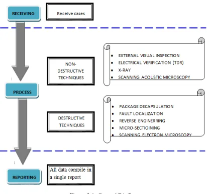
2.1 General Failure Analysis Flow
After discussing what Failure Analysis is about and some techniques that
used to determine the failure on a u nit in the previous section, a general Failure
Analysis (FA) flow is summarized in Figure 2.1.
6
2.2 Devices- Power MOSFET
Basically, MOSFET is the acronym for metal-oxide-semiconductor
field-effect transistor. It is a transistor that uses a control electrode which is called the
gate, to vary the conductance of a channel between the source and the drain.
Actually MOSFET almost same as the Bipolar Junction Transistor (BJT) where it
uses an electric field to control an output. However, the electric field not controls an
output. Rather it is controlled by a capacitor. For BJT, it only requires one kind of
charge carrier which either holes or electrons once it is activated. A MOSFET is
shown in Figure 2.2 below [2].
From Figure 2.2 above the MOSFET is consists of a substrate (p-type or n- type).
There are two islands of the other type which is called the source and the drain.
Besides that, a thin layer of silicon dioxide is on top of the islands and substrate.
And a metal electrode is over the silicon dioxide between the drain and the source
[2].
Figure 2.2: Structure of MOSFET [2]
7
One of the examples of Power MOSFET is
2.2.1 Integrated circuit (IC)
Integrated circuit is a combination of electronic circuits on a small plate surface, or “chip" which is made of semiconductor material, mostly silicon. Figure 2.5 below shows the image of an integrated circuit.
Imaging, deposition and etching are the necessary key process steps which
semiconductor ICs are fabricated in layer process.
Devices such as flip-flops, logic gates, counters, shift registers and logic ICs process
digital signals. These devices can be split into two groups referring to their pin
arrangements which are the 4000 series and the 70 series which consists of different
categories namely 74HCT, 74HC and 74LS [2]
(a) (b)
Figure 2.4: (a) Power of MOSFET (b) Symbol with notation [1]
8
.
The terms of sink or source current by IC outputs depends on the direction of the
current at the output of IC.
Current is flowing into the output if the IC is sinking current. A device connected
between the IC output and the positive supply (+Vs) will be turned on when the
output is low, which is 0V.
Current is flowing out of the output if the IC is sourcing current. A device connected
between the IC output and the negative supply (0V) will be turned on when the
output is high, which is +Vs [2].
Figure 2.7: Sinking and sourcing current [3,11]
9
2.2.2 Relay
Relays are known as an electrically operated switch as an electromagnet is used by relays to operate switching mechanisms mechanically. Where several circuits ought to be controlled by one signal and a low power signal which with complete electrical isolation between controlled circuits, relays are necessary to be used [3].
A magnetic field is generated when an electric current is passed through the coil that
armature is activated, and a connection with a fixed contact is being made or broken
by the consequent movement of the movable contacts. The movement opens the
contacts and breaks its connection if the relay is de-energized and set of contacts was
closed, and the other way round when the contacts were open. The armature will be
returned by a force, which is about half as strong as the magnetic force when the
current to the coil is switched off to its relaxed position. Normally this force is
equipped by a spring. However, gravity is also usually been used in industrial motor
starters [3].
2.3 Equipment
2.3.1 Curve Tracer
The curve tracer was basically developed as a diode and transistor tester. It
allows indication in the view of graphical of the voltage versus current
characteristics. This is helpful and essential due to the characteristics of nonlinear (b)
(a)
![Figure 2.2: Structure of MOSFET [2]](https://thumb-ap.123doks.com/thumbv2/123dok/548092.64278/21.595.225.434.624.731/figure-structure-of-mosfet.webp)
![Figure 2.4: (a) Power of MOSFET (b) Symbol with notation [1]](https://thumb-ap.123doks.com/thumbv2/123dok/548092.64278/22.595.154.475.117.299/figure-power-mosfet-b-symbol-notation.webp)
![Figure 2.7: Sinking and sourcing current [3,11]](https://thumb-ap.123doks.com/thumbv2/123dok/548092.64278/23.595.152.478.79.270/figure-sinking-and-sourcing-current.webp)
![Figure 2.8: (a) Relay (b) Structure of relay [3]](https://thumb-ap.123doks.com/thumbv2/123dok/548092.64278/24.595.143.465.219.401/figure-relay-b-structure-relay.webp)