!"
A.A Abd Aziz
1, A. Rani Othman
2, I. Ibrahim
3, S.A Sahingan
4, M.F Selamat
5and M.H Che
Halim
61,2,3,4,5
Faculty of Electronic & Computer Engineering Universiti Teknikal Malaysia Melaka (UTeM)
Locked Bag 1200, Hang Tuah Jaya, 75450 Ayer Keroh, Melaka,
Malaysia
[email protected],[email protected],[email protected]
In this paper, a simulation of cascaded LNA and RF amplifier for front7end direct conversion receiver at 5.87GHz frequency band is presented. By using direct conversion architecture, the image rejection performance is improved, lower complexity and the component is reduced. The cascading LNA and RF amplifier has 27 dB gain and 2.17 dB noise figure. The LNA and RF amplifier is simulated using Ansoft Designer software and fabricated with Duroid 5880 as the microstrip material.
! "
# $
There are many types of front7end receiver in the transceiver today. There are direct conversion receiver, directly amplifying receiver, reflectional receiver, homodyne detection, low IF receiver, tuned radio frequency receiver, superheterodyne receiver and etc. The front7ends typically combine systems operating below 2.5GHz, for example WCDMA and GSM [1]. However, due to limited capacity of these systems, frequencies above 2.5 GHz are becoming popular. Besides, to design a front7end receiver with good image rejection, lower complexity and fewer components count requiring suitable architecture of the receiver [2].
Superheterodyne and direct conversion receiver is discussed more than the other receiver architectures in this paper. Both of this architecture is compared for integrated solution in portable devices of modern wireless communication system [1]. Therefore, direct conversion architecture is mostly chosen for the integrated solution that can be implemented in ICs [2]. As a trade7off, superhetrodyne architecture has an additional system drawback; problem of image frequency. According to this problem, direct conversion architecture is chosen to overcome that problem of image frequency.
In this paper, a cascaded LNA and RF amplifier for front7end direct conversion receiver for 5.8 GHz
(WLAN) system is presented, which is good image rejection, lower complexity, less component count and low noise figure and satisfy the IEEE 802.11a standard.
% & '
Noise is a random process where it is usually characterized by using probability density function (PDF) and power spectral density (PSD) [3], [4]. It is associated with a variety of sources, including thermal noise generated by RF components and devices, noise generated by atmosphere and interstellar radiation, and man7made interference [4].
According to David M. Pozar [5], thermal noise is the most prevalent type of noise encountered in RF system where noise power of the thermal noise can be modeled as an equivalent thermal noise source and characterized by using an equivalent noise temperature,
#
:#
=$
, (1)
where,
= noise power of white noise source in Watt (W)
$ = Boltzmann’s constant, 1.380 x
10
−23 (J/K) = equivalent noise bandwidth of system in Hertz (Hz)#(
For cascaded RF components that become as a RF system (see Figure 2), noise figure of the system can be calculated if noise figure and gain of each RF component is known. The total noise figure of the RF system is known as Friss equation [6] by the given equation,
RF component
%/ % /
(
) (
)
&'= equivalent input noise factor (linear)
= stage noise factor (linear) = stage gain (linear)
%(
Equation (2) is calculated in linear form (noise factor) and then converted to logarithmic form (noise figure). Friss equation is useful if receiver employs various off7the7shelf building blocks that characterized independently by manufacturer.
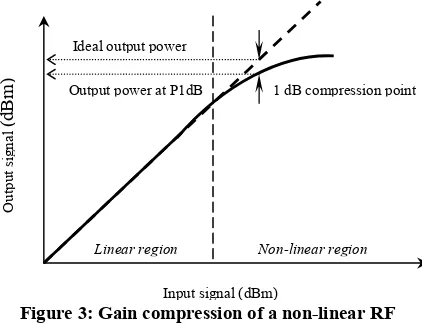
Saturation or compression occurs in all circuits because the available output power is finite [6]. This means as the signal amplitude increases, the gain begins to vary. In other words, gain compression will occur and limit the output power of RF receiver. Consequently, in RF receiver, this will limit the dynamic range of the receiver [6]. This can be depicted in Fig. 3 where output power versus input power of RF system is plotted.
1 dB compression point (P1dB) is used to quantify the linear range of RF component [6] and RF system as well. By definition, power at P1dB is the point where the output power level has decreased by 1dB from the ideal characteristic [6]. Therefore, gain compression measurement and analysis are essential in RF system in order to see the response of output power due to non7linearity of the system.
)(
*
Third order intercept point (IP3) is defined as the theoretical point at which the IM3 products and the desired signal intercept each other with equal value in signal level (see Fig. 4). IP3 is used as a measure of
circuit or system linearity [7] by calculating the output power level of IM3 products from two input signals, which very close to each other (see Figure 5). This method is called two7tone test [7] where output IP3 (OIP3) can be calculated by the given equation [10],
OIP3 = A + /2, (3)
where,
()*+= output third order intercept point (dBm) = level of RF output signal at RF system port (dBm)
= difference between desired RF output signal with IM products (dBc)
+( &,
*
( $-) $.) ' *
In RF receiver, sensitivity is one of the most important parameter to be considered when designing a RF system. That is because RF receiver receives very weak intended radio signal, which is very close to noise level. Sensitivity is defined as the minimum signal level that the system can detect with acceptable signal7to7noise ratio [5]. In wireless digital communication system, sensitivity is the minimum
,
1 dB compression point Output power at P1dB
received signal level that produces a specified BER when the signal is modulated with a bit sequence of data.
Sensitivity equation is derived from noise figure equation [5] [6] [7]. To calculate sensitivity, equation (5) rewritten as
The receiver’s sensitivity is limited by IF bandwidth, noise figure and minimum SNR. IF bandwidth is usually fixed on the channel bandwidth used in the RF system
.
The level of minimum SNR for receiver sensitivity depends on the type of modulation (i.e. QPSK, BPSK and167QAM) [7] because SNR is related with bit energy to noise power spectral density,120 of the modulation. Therefore, in RF system design, noise figure plays an important role to ensure that the value of noise figure does not reduce the sensitivity of RF system.
)
-Direct conversion, also known as homodyne or zero7IF conversion, is a natural approach to convert an RF signal directly to baseband. Alternately, one can think of choosing IF to be zero. The architecture of the propose project of my communication group is depicted in Figure 7.
/( . 0
,
The propose architecture is comprise the individual RF components such as LNA, RF amplifier, power divider, and band7pass filter. In this paper, we just concern to main RF component, that is, LNA and RF amplifier. For the whole operation of receiver as depicted in Figure 6 are starts at the antenna. The signal from the antenna then guided to Low Noise Amplifier.
Low noise amplifier is an important part where it deals with noise; noise characteristics of the first stage of receiver exert a large influence on the entire system. Besides remove noises, LNA also act as pre7amplifier
before RF amplifier. Then noise reduced signal will be amplified by RF amplifier. ]
The IEEE 802.11a standard is used as references. The Low Noise Amplifier (LNA) system should meet this standard requirement and should operate properly for WLAN Bridge system [8]. The main requirements of the LNA are the lowest possible noise figure (NF) with a reasonable gain. The general topology of the LNA consists of three stages: the input matching network (IMN), the amplifier itself and the output matching network (OMN) [9], [10], [11]. The 5.8 GHz wireless LAN market grows rapidly and offers various benefits to the user. 5.8 GHz WLAN technology supports multimedia services, real time voice and video transfer and other bandwidth intensive applications [12].
A low noise amplifier (LNA) is first RF block in any receiver chain. This paper presents two different designs of a LNA at 5.8GHz. The circuit design starts from FHX76LP Low noise SuperHEMT device designed for DBS application from Eudyna Device USA Inc amplifier using the microstrip technology. It is the LNA that mainly determines the noise figure of the system. Low power dissipation and small integrated area are also some important factors that must be considered in the design of the devices for wireless applications [13]. Based on S7parameters of the transistor and certain performance requirements, a systematic procedure is developed for the design of LNA. In LNA design, the most important factors are low noise, moderate gain, matching and stability [14]. Besides those factors, power consumption and layout design size also need to be considered in designed works. Figure 7 shows the LNA schematic.
1( 0 ,
power microwave ovens, cordless phones, Bluetooth® and HomeRF applications, WLAN, game pads, etc. As a consequence, significant RF interference is present within the 2.4 GHz band [15]. Recently, wireless LAN system have been developed for the C7band (4~8 GHz) frequency. Proposals for wireless data system in the C7 band range such as 5.8 GHz (Wireless LAN for U.S.A) and 5.2 GHz (Hiper LAN for Europe) have been submitted [16]. The license7free 5.8 GHz frequency band provides wider spectrum frequency. Furthermore, investigations showed that 5 GHz applications in narrow surroundings can provide better performance than 2.4 GHz applications as the shorter wave length propagates further. In addition, 5.8 GHz system nearly always be operated at higher data rates than 2.4 GHz systems in form of bandwidth [17].
The power amplifier is the most important and expensive device in the RF block of Wireless LAN system [18]. Like all other amplifiers, stability is a major concern [19]. This paper is focused on the development of RF amplifier for point7to7point WLAN application. A single7stage RF amplifier is fabricated using HFET on GaAs substrate. The size of the circuit is reduced by utilizing high dielectric substrate. Figure 8 shows the block diagram of RF amplifier module and Figure 9 shows the schematic of RF amplifier.
( 2 3 4%56
7( ,
+
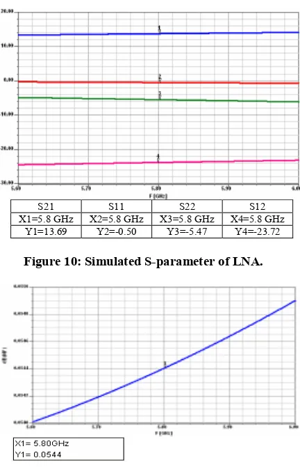
The simulations have been done individually of each LNA and RF amplifier. Then the cascading of LNA and RF amplifier were simulated. The simulation result of LNA, RF amplifier and cascaded LNA and RF amplifier are presented in Table 2
& 8 #(
Parameter LNA
(dB)
RF Amplifier
(dB)
LNA & RF Amplifier
(dB)
S21(Gain) 13.69 14.62 27.44
NF (Noise
Figure) 0.0544 7 0.27
S11(Input
Return Loss) 0.50 710.98 0.20
S22(Output
Return Loss) 75.47 74.76 73.44
As depicted in Table 1, we can see that the gain for both LNA and RF amplifier are high. For noise figure, it shows that small noise figure, that is, it below than 2 dB. Hence, these satisfy the standard to design a RF receiver.
S21 S11 S22 S12
X1=5.8 GHz X2=5.8 GHz X3=5.8 GHz X4=5.8 GHz
Y1=13.69 Y2=70.50 Y3=75.47 Y4=723.72
#5(
S21 S22 S11 S12 X1=5.8 GHz X2=5.8 GHz X3=5.8 GHz X4=5.8 GHz
Y1=14.62 Y2=74.77 Y3=710.97 Y4=723.71
#%(
S21 S11 S22 S12
X1=5.8 GHz X2=5.8 GHz X3=5.8 GHz X4=5.8 GHz
Y1=27.44 Y2=0.20 Y3=73.44 Y4=748.30
#)(
8
The LNA and RF amplifier circuits will be fabricated by a manufacturer because lack of instruments and tools for this purpose. The designed circuit will also tune and optimized by the manufacturer in order to get an optimum layout. Somehow, the performances of the simulated circuit will be remained.
/
A cascaded LNA and RF amplifier for RF front7 end direct conversion receiver is presented in this
paper. This LNA and RF amplifier can be apart of WLAN receiver architecture since it fulfill the IEEE 802.11a standard. In this project also, direct conversion architecture is chosen because it will give the good image rejection, lower complexity, less component count and low noise figure and satisfy the IEEE 802.11a standard.
[1] G. Schultes, P. Kreuzgruber, A.L Scholtz, “DECT Transceiver Architectures: Superheterodyne or Direct Conversion?”
3 4 !'& # 4 ' . 5 % &! !
May 1993, pp. 953 – 956.
[2] S. Mirabbasi and K. Martin, “Classical and Modern Receiver Architectures”, )111
5 66! & /&.& , pp. 132 – 139,
November 2000.
[3] B. Razavi, / ' , Prentice Hall, 1998.
[4] M. Madihian, et al., “L7C7 Band Low7Voltage BiCMOS MMIC’s for Dual Mode Cellular7 LAN Applications”, )111 # & &
/ & #4 & # 4 7! , vol. 44, No.
11, November 1996, pp. 202572031.
[5] David M. Pozar, / & & ' % 6, Third Avenue, N.Y, John Wiley & Sons, Inc, 2000.
[6] A. Parssinen, 5
& % 6 , Kluwer Academic
Publishers, 2001.
[7] David M. Pozar,/ & 1 . ., Third Edition, John Wiley & Sons, Inc., 2000. [8] H. Jin and C.A.T. Salama, “A 17V, 1.97 GHz
CDMA, CMOS on SOI, Low Noise Amplifier,”
in * . -""" )111 ) & &' %()
5 ( -""" 88 ,"- ,"+.
[9] TH. Lee, #4 . 5/(% &
7! ) . & 5 ! , Cambridge
University Press, 2006.
[10] B7J. Jang, I7B. Yom, S7P. Lee “V7Band MMIC Low Noise Amplifier Design Based on Distributed Active Device Model,” in
* . */5-"",, #& 8 #& &
( 5, IEEE 2001, pp. 25728.
[11] S. Park and W. Kim, “Design of a 1.8 GHz Low Noise Amplifier for RF Front7End in a 0.8Um CMOS Technology,” )111 # & &
5 !6 1' vol. 47, No. 1, February 2001.
[12] A. Parssinen, S. Lindfors, J. Ryynanen, S.I. Long, and K. Halonen, “1.8 GHz CMOS LNA With On7Chip DC Coupling for a Subsampling Direct Conversion Front7End,” in * .
4 ,99 )111 ) & &' % 68 !6
[13] D.M. Pozar, “Microwave and RF Wireless System”, United States of America: John Wiley and Sons Inc. 77797, 2057207, 2000.
[14] G. Gonzalez,/ & # & 68'
&' & . , 2ndEdition, Upper Saddle
River, NJ: Prentice – Hall Inc. 217, 2947303, 1997.
[15] B. Alexander, and F. Smith, “WiFi (IEEE802.11b) and 2.4 GHz Wireless Telephone System”, 4 *&8 5 % 6, May 2001.
[16] U. Lott, “Low DC power monolithic low noise amplifier for wireless application at 5 GHz,”
)111 / & & / '' 6 &
/ ' 4 5 ! % 68 !6 pp. 81784, 1998.
[17] J. Geiger, “802.11a/b Site Survey: A Testimonial”,http://www.wifiplanet.com/colum ns/article.php/1479831, December 2004. [18] H. K. Choi, et. al., “The Design of Power
Amplifier for 5.8 GHz Wireless LAN Application Using GaAs Substrate”,/ &
5 & *& , 2000.
[19] M. Romney and S. Farahvash, “Integrating a SiGe BiCMOS Power Amplifier in a 5.8GHz Transceiver”, IEEE 2006.
[20] N. Suematsu and S. Shinjo, “CMOS/BiCMOS Power Amplifier Technology Trend in Japan”,