DOI: 10.12928/TELKOMNIKA.v13i4.1894 1145
FPGA Implementation ofLow-Area Square Root
Calculator
Aiman Zakwan Jidin*1, Tole Sutikno2 1
Faculty of Engineering Technology, Universiti Teknikal Malaysia Melaka 2Department of Electrical Engineering, Universiti Ahmad Dahlan
*Corresponding author, e-mail: [email protected], [email protected]
Abstract
Square root is one of the mathematical operations which are widely used in digital signal processing. Its implementation on hardware such as FPGA will provide several advantages compare to the performance offered in software. There are several algorithms which can be utilized for this calculation, but they are difficult to be implemented in FPGA. This paper presents a model of FPGA based square root calculator, which requires very low resources usage, thus occupying very low area of FPGA. The model is designed to suit the needs of medium-speed and low-speed applications which don’t need very high processing speed, while optimizing the number of resources utilized. The modified non-restoring algorithm is used in this design to compute the square root. The design is coded in RTL VHDL, and implemented in Altera DE2-board for hardware validation. The implementation produced very precise square root calculation, with low latency computation and low area consumption, for various input data width tested.
Keywords: FPGA, VHDL, Square Root, Area Optimization
Copyright © 2015 Universitas Ahmad Dahlan. All rights reserved.
1. Introduction
Square root is an arithmetic operation which is widely used in various applications such as image and audio processing, scientific computation, computer graphics and digital communications [1- 2- 3- 4]. Recently, there are many researches which implement the square root calculator in hardware like Field Programmable Gate Array (FPGA) in order to achieve high speed computation. The main interest of implementing square root calculation in hardware is to reduce the delays present in its computation, thus producing a very fast computation.
In many VLSI applications nowadays, it is vital to create designs which are not only producing correct and accurate results, but also to provide designs with very high processing speed, where the execution delay is typically in the order of a few nanoseconds or even faster, like in the case of a computer graphic applications. However, in order to achieve the best performance from the system, certain criterias like the power consumption and the resources utilization need to be sacrificed.For instance, the computation speed in hardware can be increased by introducing techniques such as pipelining and parallel computing [5]. The latter will certainly speed up the process, however creating multiple parallel path for the same operation will cause the increase in the number of resources (i.e. Adders, Registers) used, and in consequence, the area or the size of the design will also become bigger.
This case is certainly becoming an unnecessary issue which is encountered when developing medium-speed and low-speed applications, with the sampling or operating frequency is less than 10MHz, which do not required very high speed computation with very small delays, while still need to utilize the same amount of resources and thus occupying the same area in the hardware. For example, applications like Direct Torque Control (DTC) for machines, which implemented the square root calculation in FPGA to achieve better estimation of flux and torque, only operated at a minimum sampling period of 5 µs [6]. In this case, the redundancy which had been introduced by the parallel computation can be eliminated and therefore, optimizing the resources usage.
capability to reduce the number of hardware resources utilization, since it does not restore the remainder [13- 14].
This paper presents an effective way to design a low-area square root calculator, which is implemented by using FPGA. The main contribution of this paper is the development of the square root calculator by using the modified non-restoring method, which is coded in synthesizable VHSIC Hardware Description Language (VHDL). In addition, the implementation strategy proposed in this paper is by sharing common hardware resource, thus eliminating circuit redundancy and optimizing the design area. In the result and analysis section, the performance of the proposed design, in terms of resources usage, speed, latency and also power dissipation, will be analyzed and compared to those obtain from the non-optimized design, which was developed previously by using the same algorithm [13].
2. Research Method
In this section, the theory of the algorithm for computing square root results in hardware is explained. Next, the implementation stratergy in FPGA will be described. The whole implementation is designed by using VHDL. All digital computations are performed in unsigned binary, since square root can only accept positive numbers as the radicand.
2.1. Modified Non-Restoring Method
A square root equation can be written as follows:
√ (1)
Where D is the radicand, and Q is square root of D. In digital computation, D is denoted by n-bit unsigned number, represented as D = Dn-1Dn-2…D1D0. For every pair of bits of the radicand, the integer part of the square root has one bit. Therefore, the resulted square root Q should be represented by m = n/2 bits: Q = Qm-1Qm-2…Q1Q0.
In the conventional non-restoring digit-by-digit calculation, only a pair of bits from the radicand is taken in order to compute the partial square root result at each iteration, starting from the the most significant bit. This pair is appended to the current remainder, which is properly shifted first. The procedure consists of appending 01 to the partial square root obtained so far. It is properly shifted and then subtracted from the current remainder. If the newly resulted remainder is positive, then the newly developed square root bit is 1, else the bit is set to 0 and the 11 is appended to the current partial square root and an additional operation will be performed at the next iteration, instead of subtraction. The operation will keep on iterating until the last bit of the square root is calculated.
Figure 1. The example of non-restoring digit-by-digit calculation to compute the square root of 169
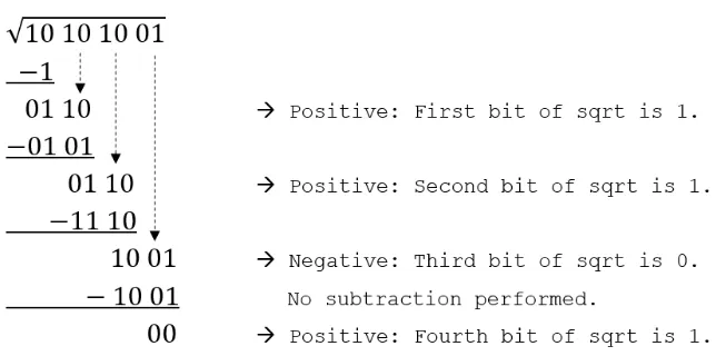
However, there is slight differences which can be found in the modified non-restoring algorithm when solving a square root problem, it provides simpler solution which only perform subtract operation and appends 01. Thus, the adding operation is removed and thus lesser hardware resources are required here. In this case, if the resulted result is negative, no subtraction will take place. As illustrated in Figure 2, the same calculation is done as the previous, by using the modified non-restoring algorithm.
Figure 2. The example of modified non-restoring digit-by-digit calculation to compute the square root of 169
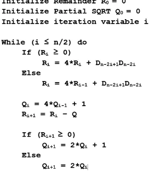
Figure 3. The pseudocode of modified non-restoring digit-by-digit calculation to solve square root computation
2.2. Hardware Implementation Strategy
As can be seen from the algorithm which has been explained in Section 2.1, the square root calculator design can partitioned into two different groups, namely Partial Remainder Calculator (PRC), which calculates the remainder value, and Partial Square Root Calculator (PSC), which determines the value of each bits in the square root result.
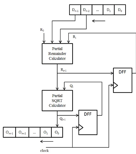
In order to achieve a very high speed square root calculation in hardware, pairs of PRC and PSC blocks shall be implemented in parallel, where each pair is used to calculate the partial square root result generated by each pair of bits of the radicand. The number of pairs to be implemented depends on the number of bits of the radicand; n-bit radicand requires the implementation of n/2 pairs of PRC and PSC in parallel. Figure 4 illustrates the block diagrams of the hardware implementation for a square root calculator with 8-bit radicand.
Figure 4. The hardware implementation of 8-bit radicand square root calculator
which is common to all computation of square root bits. This method will eliminate all the redundant circuity in the design, and thus will significantly reduce the hardware resources usage, especially for the case of square root calculators with big radicands.
Figure 5 shows the block diagrams representing the hardware implementation of low-area square root calculator. In order to allow the hardware sharing, each computation of the square root bit will be conducted sequentially. Consequently, some latency will be introduced in the square root calculation time, as only one bit of the square root is resulted at each clock cycle.
Figure 5. The hardware implementation of area-optimized square root calculator
The computation latency can be determined by looking at the number of bits used for the radicand. For n-bit radicand, the square root calculation shall be completed after n/2 clock cycles. Even the proposed implementation provides slower square root calculator than previous researches, it should be suitable for applications which do not require very high speed processing time, while the area of the design or the hardware resources utilization can be optimized.
3. Results and Analysis
The proposed design was successfully implemented on Altera DE2 Development Board, which use Cyclone II FPGA.Synthesizable VHDL code is used to configure the design. Moreover, the design coding method make it scalable, thus it is very simple to vary the width of the square root radicand in order to perform different tests.
3.1. Functional Simulation Verification
In order to verify the functionality and to analyze the performance of the design, several simulations and also hardware verification by using FPGA had been conducted.
Meanwhile, Figure 7 shows the 8-bit radicand square root calculation results which had been obtained from the hardware validation, by using FPGA. Both the radicand and the output from FPGA have been displayed in the SignalTap II Logic Analyzer. Based on these results, it shows that the square root has been correctly implemented in FPGA hardware, producing accurate results.
Figure 7. The hardware validation result of square root computed by the proposed design, displayed in SignalTap II Logic Analyzer
3.2. Design Performance Analysis
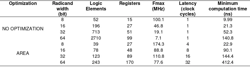
Table 1 shows the resource utilization and the processing time for various configuration tested.These data are obtained from the compilation report, which had been generated once the design compilation is completed in Altera Quartus II Software.From this table, we can clearly see that the number of logic elements (LE) used in area-optimized designs are much lower than those used in speed-optimized designs, although the number registers utilized are slightly bigger.
In term of computation time, the speed-optimized designs produce the results faster than the area-optimized design. The calculation of the minimum computation time above is based purely on the Fmax obtained, where
Minimum computation time = Latency * 1 / Fmax (2)
If the same clock frequency is used for both speed-optimized and area-optimized designs, the computation time for the former shall be n/2 times bigger than the computation time of the latter, where n is the width of the radicand in bit.
3.3. Power Dissipation Analysis
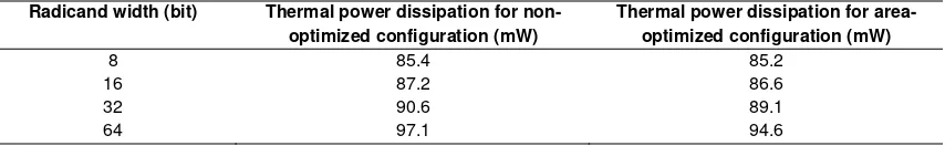
Since area-optimized configuration produced smaller design with fewer resources than non-optimized configuration, the power consumption in the former shall be lesser than the latter, as proven in Table 2.The information shown in this table are collected from the PowerPlay Power Analyzer Tool, which is a feature that is available in Altera Quartus II Software. This will certainly contribute in overcoming the problem of overheating, which has been encountered by many applications.
Table 2. The comparison of power dissipation between non-optimized and area-optimized square root design
Radicand width (bit) Thermal power dissipation for non-optimized configuration (mW)
This paper has described an alternative in the hardware implantation of a square root calculator which consume low design area or low hardware resources utilization, with low power dissipation, by using the modified non-restoring algotirhm. The design functionality has been verified via simulations and also hardware verification by using FPGA, where it produced correct and accurate outputs. The analysis also shown improvement offered by proposed design, in terms of resources usage as well as the power consumption. Despite being slower than other previous designs, it may well contribute in low-speed application which may require low design area and low power consumption.
References
[1] Vijeyakumar KN, Sumathy V, Vasakipriya P, Dinesh Babu A. FPGA implementation of Low Power High Speed square root circuits. IEEE International Conference on Computational Intelligence & Computing Research (ICCIC). Coimbatore. 2012: 1-5.
[2] Kachhwal P, Rout BC. Novel square root algorithm and its FPGA Implementation. International Conference on Signal Propagation and Computer Technology (ICSPCT). Ajmer. 2014: 158-162. [3] Yamin L, Wanming C. Implementation of Single Precision Floating Point Square Root on FPGAs.
IEEE Symposium on FPGA for Custom Computing Machines. Napa. 1997: 226-232.
[4] Xiaojun W. Variable Precision Floating-Point Divide and Square Root for Efficient FPGA Implementation of Image and Signal Processing Algorithms. PhD Thesis. Boston: Northeastern University Boston, Massachusetts; 2007.
[5] Xiumin W, Yang Z, Qiang Y, Shihua Y. A New Algorithm for Designing Square Root Calculators Based on FPGA with Pipeline Technology. Ninth International Conference on Hybrid Intelligent Systems. Shengyang. 2009; 1: 99-102.
[6] Sutikno T, Idris NRN, Jidin AZ, Jidin A. A Model of FPGA-based Direct Torque Controller. TELKOMNIKA Indonesian Journal of Electrical Engineering. 2013; 11(2): 747 – 753.
Vedic Mathematics. International Journal of Information & Computation Technology. 2014; 4(15): 1531-1537.
[13] Sutikno T, Jidin AZ, Jidin A, Idris NRN. Simplified VHDL Coding of Modified Non-Restoring Square Root Calculator. International Journal of Reconfigurable and Embedded Systems. 2012; 1(1): 37-42. [14] Rahman A, Abdullah AK. New efficient hardware design methodology for modified non-restoring