PRODUCING CaCu3Ti4O12 DOPED LANTHANUM (III)
ACETATE HYDRATE VIA SOLID STATE REACTIONS
HARIS FAHAZA GHAZALI
B050810117
UNIVERSITI TEKNIKAL MALAYSIA MELAKA
UNIVERSITI TEKNIKAL MALAYSIA MELAKA
PRODUCING CaCu
3Ti
4O
12DOPED LANTHANUM (III)
ACETATE HYDRATE VIA SOLID STATE REACTIONS
This report submitted in accordance with requirement of the Universiti Teknikal Malaysia Melaka (UTeM) for the Bachelor Degree of Manufacturing Engineering
(Engineering Materials)
by
HARIS FAHAZA BIN GHAZALI
B050810117
UNIVERSITI TEKNIKAL MALAYSIA MELAKA
BORANG PENGESAHAN STATUS LAPORAN PROJEK SARJANA MUDA
TAJUK:
Producing CaCu
3Ti
4O
12Doped Lanthanum (III) Acetate Hydrate
via Solid State Reactions
SESI PENGAJIAN: 2010/11 Semester 2
Saya HARIS FAHAZA B. GHAZALI
mengaku membenarkan Laporan PSM ini disimpan di Perpustakaan Universiti Teknikal Malaysia Melaka (UTeM) dengan syarat-syarat kegunaan seperti berikut:
1. Laporan PSM adalah hak milik Universiti Teknikal Malaysia Melaka dan penulis.
2. Perpustakaan Universiti Teknikal Malaysia Melaka dibenarkan membuat salinan
untuk tujuan pengajian sahaja dengan izin penulis.
3. Perpustakaan dibenarkan membuat salinan laporan PSM ini sebagai bahan
pertukaran antara institusi pengajian tinggi. atau kepentingan Malaysia yang termaktub di dalam AKTA RAHSIA RASMI 1972)
DECLARATION
I hereby, declared this report entitled “Producing CaCu3Ti4O12 Doped Lanthanum (III) Acetate Hydrate via Solid State Reactions” is the result of my own research
except as cited in references.
Signature : ...
Author’s Name : HARIS FAHAZA BIN GHAZALI
APPROVAL
This report is submitted to the Faculty of Manufacturing Engineering of UTeM as a partial fulfilment of the requirements for the degree of Bachelor of Manufacturing Engineering (Engineering Materials). The member of the supervisory committee is as follow:
i
ABSTRAK
ii
ABSTRACT
iii
DEDICATION
This dedication goes to my beloved mom’s and my late father’s, Fauziah Bt. Saad and Ghazali B. Ismail
a very supportive siblings,
Hafiz Fahaza B. Ghazali, Nadzirah Fahaza B. Ghazali, Hasyraf Fahaza B. Ghazali, Hezry Fahaza B. Ghazali
and especially Norshafiza Bt. Abu Bakar and not forget to all my dearest friends,
iv
ACKNOWLEDGEMENT
First and foremost, I am very grateful to Allah S.W.T for giving me strength, patience and blessing throughout my period to complete my final year project (Projek Sarjana Muda I and II).
I would like to record my appreciation to Dr. Mohd Warikh Bin Abd Rashid for his continuous supervision, encouragement, knowledge and making innumerable suggestions for clever ways to elucidate this thesis and entire period of research. Without him this thesis is never be completed.
And not forgetting to all my mates, Universiti Teknikal Malaysia Melaka laboratory technicians and individual, who always helps with brilliant ideas and discussion until I finished my final year project.
Finally, I treasure the warmth and love with highly appreciation and dedication to my
family, without their support and sacrifice; I won’t be here to complete my study in Universiti Teknikal Malaysia Melaka.
v
2.1.1 Structure of CaCu3Ti4O12 (CCTO) 6
2.1.2 The Origin of Dielectric Behavior of CCTO 7
2.1.3 Role of Doping 8
2.1.4 Barrier Layer Capacitors 9
2.2 Ceramic Materials 10
2.2.1 Ceramic Structure 12
2.2.2 Crystal Symmetry 13
2.2.3 Ceramics Crystalline of Partially Crystalline Materials 15
2.3 Electroceramic 15
2.3.1 Ferroelectric Ceramics 16
2.3.2 Piezeoelectric Ceramics 17
vi
2.4 Dielectric Strength 19
2.4.1 Intrinsic Dielectric Strength 20
2.5 Perovskite Composition 20
2.5.1 Crystallography of the Perovskite Structure 20
2.12 Scanning Electron Microscope (SEM) 26
vii
CHAPTER 4: RESULT AND DISCUSSIONS 36
4.2 LCCTO Characterizations 36
4.3 Observation on Sample Preparation Process 40
4.3.1 Particle Volume Average 43
4.3.2 Manually Hand Pressed Pellets 44
4.3.3 Optical Microscope Observation of Green Body 46
4.3.4 SEM Observation on Green Body 47
4.4 Calcinations 48
4.5 Sintering 52
4.5.1 Shrinkage and Defect Observation 53
4.5.2 Sample Observation by Using SEM 55
4.6 Micrograph Study on SEM Image after Sintering Process 64
4.7 Conductivity 65
4.8 Density Test 66
4.9 EDX Test on Failure Samples 67
CHAPTER 5: CONCLUSION AND RECOMMENDATIONS 70
viii
LIST OF TABLES
2.1: Pattern structure of several mineral structures 13
2.2: Point groups for the seven crystal system 14
2.3: Lanthanum properties 28
4.1: Particle Size of LCCTO 0.03wt% 41
4.2: Particle Size of LCCTO 0.05wt% 41
4.3: Particle Size of LCCTO 0.07wt% 41
4.4: Average particle volume 0.03wt% 43
4.4: Average particle volume 0.05wt% 43
4.5: Average particle volume 0.07wt% 44
4.4: Optical Microscope observed of LCCTO on green body 46
4.5: Calcine parameter 48
4.6: Optical microscope morphological study on LCCTO 800°C
for 12h Calcination 49
4.7: Optical microscope morphological study on LCCTO 900°C
for 12h Calcination 50
4.8: Optical microscope morphological study on LCCTO 1000°C
for 12h Calcination 51
4.9: Sinter parameter 52
4.10: Shrinkage percentage of LCCTO after sintering process 54
4.11: Conductivity Result on LCCTO 65
ix
LIST OF FIGURES
2.1: Structure of CaCu3Ti4O12 (CCTO) 7
2.2: Taxonomy of ceramics 11
2.3: Perovskite structure 20
3.1: Flow chart of methodology 31
4.1: Micrograph of the LCCTO with 0.03wt% doping percentage 37 4.2: Micrograph of the LCCTO with 0.05wt% doping percentage 37 4.3: Micrograph of the LCCTO with 0.07wt% doping percentage 37 4.4: The element in LCCTO composition observed with XRD
(a) LCCTO 0.03wt%, (b) LCCTO 0.05wt%, (c) LCCTO 0.07wt% 38
4.5: LCCTO powder after mixing 40
4.6: Green Body 45
4.7: Dimension of green body 45
4.8: The scanning electron microscope (SEM) of the green body LCCTO 0.03wt% after the pellet pressed;
(a) outer surface and (b) defect on surface 47
4.9: Sintering profile 52
4.10: Defect occurred after sintering process 53
x
4.20: Doping 0.03wt%, Calcine 900°C, Sinter 1100°C, 24 hours 58 4.21: Doping 0.05wt%, Calcine 900°C, Sinter 1100°C, 24 hours 58 4.22: Doping 0.07wt%, Calcine 900°C, Sinter 1100°C, 24 hours 58 4.23: Doping 0.03wt%, Calcine 1000°C, Sinter 1100°C, 12 hours 59 4.24: Doping 0.05wt%, Calcine 1000°C, Sinter 1100°C, 12 hours 59 4.25: Doping 0.07wt%, Calcine 1000°C, Sinter 1100°C, 12 hours 59 4.26: Doping 0.03wt%, Calcine 1000°C, Sinter 1100°C, 24 hours 60 4.27: Doping 0.05wt%, Calcine 1000°C, Sinter 1100°C, 24 hours 60 4.28: Doping 0.07wt%, Calcine 1000°C, Sinter 1100°C, 24 hours 60 4.29: Doping 0.03wt%, Calcine 800°C, Sinter 1100°C, 6 hours 61 4.30: Doping 0.05wt%, Calcine 800°C, Sinter 1100°C, 6 hours 61 4.31: Doping 0.07wt%, Calcine 800°C, Sinter 1100°C, 6 hours 61 4.32: Doping 0.03wt%, Calcine 1000°C, Sinter 1100°C, 6 hours 62 4.33: Doping 0.05wt%, Calcine 900°C, Sinter 1100°C, 6 hours 62 4.34: Doping 0.07wt%, Calcine 900°C, Sinter 1100°C, 6 hours 62 4.35: Doping 0.03wt%, Calcine 1000°C, Sinter 1100°C, 6 hours 63 4.36: Doping 0.05wt%, Calcine 1000°C, Sinter 1100°C, 6 hours 63 4.37: Doping 0.07wt%, Calcine 1000°C, Sinter 1100°C, 6 hours 63
4.38: Sample failure at 1200°C Sintering 64
xi
LIST OF ABBREVIATIONS
CRT - Cathode Ray Tube
EDX - Energy-dispersive X-ray Spectroscopy EIS - Electrochemical Impedance Spectroscopy FCC - Face Centred Cubic
ILBC - Internal Barrier Layer Capacitors IS - Impedance Spectroscopy
LCR - (Inductance (L), Capacitance (C), and Resistance (R)) PLZT - Lead Lanthanum Zircornate Titanate
PMN - Lead Magnesium Niobate PZC - Point Zero Charge
PZT - Lead Zirconate Titanate RS - Rochelle salt
1
CHAPTER 1
INTRODUCTION
1.1 Introduction
The introduction will slightly brief the purpose of produce Lanthanum (La) doped CaCu3Ti4O12 (CCTO) powders. Methods, process and also research study in doping materials developed for La doped CCTO will also covered. In the previous research done the other researchers in produce CCTO, Calcium (Ca) is used as base material. This purpose of research studies will try to doping the base materials alternatively use La and to get a result whether dielectric materials can be produce, in other hands to get a better dielectric material than CCTO. The properties in this compound will have a differential then others doped CCTO produce with other researchers, because it depending on the parameters or doping materials state by the researcher.
Recently, the interest in produce Calcium Copper Titanium Oxide (CaCu3Ti4O12) as new generation of ultrahigh dielectric materials was choose because of its good dielectric properties. These materials have been demonstrated to have a dielectric constants as high as Ɛ = 80,000 for single crystal structure at room temperature and remains constant over 100 - 600K at low frequencies (Fadhlina, 2007) (Bozin et al., 2004). Dielectric materials have many technological applications in electronic devices such as capacitors, resonators, and filters.
2
1.2 Problem Statement
Lanthanum (La) doping was introduced into CaCu3Ti4O12 (CCTO) in order to improve the dielectric properties. Some methods in generating La doped CCTO such as wet chemistry and sol-gel has identified and studied based on microstructure development. The solid state reaction method was choose in producing La doped CCTO ceramics after agree with some researchers. Most of the reports are done on this material said, it were prepared by solid state reaction from metal oxide at higher temperature with several intermediate grinding such as by using ball milling. The reason for studying this doping is to prove that with the correct parameters, La doped CCTO can be produce and resulted in the desired formation of the nanocrystalline and eliminate the factors that may influence the unwanted phase and impurities. Solid state reaction requires tedious work, relatively long reaction times for sintering such as 1000°C overnight, 1000°C for 20 hours, 1000°C for 24 hours (Liu et. al., 2007) and high temperature conditions and still may result in unwanted phase because of limited atomic diffusion through micrometer sized grain (Sen et al., 2010). The observation on the different samples with different parameters need to be analyze by using the XRD to determine the effect of parameters using and microstructure patterns of the La doped CCTO ceramics.
3
up to two orders of magnitude (from 104 to 102), and the nonlinear varistor characteristics disappear completely, which should be mainly ascribed to the decrease of potential barrier height at the grain boundary and charge compensation for the conduction electrons caused by the doping (Cai et. al., 2007), Eu2O3 doping can reduce the mean grain size and can also deter the formation of Cu-rich phases at the grain boundaries (Li et. al., 2009), Zircornium (Zr) substituting experimental results indicated that there is no obvious effect on microstructure characteristic (Cai et. al.) and several more materials such as; tin oxide (SnO2), Nickel (Ni), Sodium
(Na), Iron (Fe), Cobalt (Co).
Doping of higher charge, like a La ions, enhance domain wall mobility and result in improved remaining polarization, coupling factors, dielectric constants, dielectric loss tangent and increased of optical transparency of electrically material. The measurement and characterization results of stoichiometric CCTO clearly indicated that the dielectric properties, evolution of secondary phases, and microstructures were strongly dependent upon the processing parameters (Kwon, 2008). Characterization of the Lanthanum (La) doped ceramics with XRD and SEM showed average grain sizes 1-2µm, indicating La amount to have little impact on grain size. Compared with CCTO, La doped CCTO showed a flatter dielectric constant curve related to frequency, it was found that the loss tangent of the ceramics composition of La(2/3)xCa1-xCu3Ti4O12 (LCCTO) less than 0.20 in 600x105 Hz region, which rapidly decreased to a minimum value of 0.03 by Ladoping with 0.05wt%. The Ɛmax value became considerably high, which was almost higher than that of sample with 0.00wt%. The curves about Ɛ values of samples with 0.05 - 0.15wt% were fairly flat while the curves of 0.20wt% and 0.00wt% were much steeper (Patra, 2009).
1.3 Objective
4
The scopes of the study will divide into three major difficulties that are;
5
For part B, the mixed powder then calcine at temperature determine at 1200°C for 12 hours to produce single phase CCTO (Patra, 2009). The temperature of calcination was chosen high enough to cause complete reaction. The objective of choosing calcinations temperature and suitable soaking time is to develop perovskite structure without any additional element. The composition represent in the powder is observed using X-ray diffraction (XRD) to determine the compositions develop, while scanning electron microscope (SEM) is use to inspecting micrographics and phases of samples.
6
CHAPTER 2
LITERATURE REVIEW
2.1 Introduction
This chapter reviews related study done the researcher in producing electroceramics through solid state reaction method. This literature reviews are mainly focused in the material selection for the doping and its parameters significant to achieved perovskite structure and high electric permittivity. The effect of suitable composition will be further reviewed based on the doped material. Electroceramics can now broadly describe that ceramic material have been specially formulated for specific electrical, magnetic or optical properties. A new generation in electroceramics can be used to obtain composite with the better performance indispensable dielectric properties for modern electronic devices. In general, these compounds belong to perovskite structure where high electric permittivity is always associated with ferroelectric or relaxor properties (Sen et al., 2010). Ceramic materials and single crystals showing ferroelectric behaviour are being used in many applications in electronics and optics. A large number of applications of ferroelectric ceramics also exploit properties that are an indirect consequence of ferroelectricity, such as dielectric, piezoelectric, pyroelectric and electro-optic properties (Ahmad et al., 2000).
2.1.1 Structure of CaCu3Ti4O12 (CCTO)
7
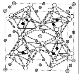
CCTO ceramics considerable as ferroelectric perovskite oxide ceramics has the isometric structure with cubic space group lm3 (Fadhlina, 2007).
Figure 2.1: Structure of CaCu3Ti4O12 CCTO showing tilted oxygen octahedra. White, light, dark, and
black atoms are O, Ca, Cu, and Ti, respectively. Dashed lines indicate 40-atom primitive cell of
antiferromagnetic spin structure (He et. al., 2002)
Its structure can be derived from the ideal cubic perovskite structure by superimposing a body centred ordering of Calcium (Ca) and Copper (Cu) ions and a pronounced tilting of the titanium centred octahedral (tilt system a+a+a+ ) can be interpreted in the terms of lattice modes (Bozin et al., 2004).
2.1.2 The Origin of Dielectric Behaviour of CCTO
8
temperature dependent and undergo a maximum in the vicinity of the ferroelectric to paraelectric transition temperature. The microstructure and impedance characteristic of CCTO were found strongly dependent on the sintering conditions. CCTO is a property that could make the material ideal for use in capacitors. CCTO ceramics are constituted of semi-conducting grains (pure CCTO phase) and insulating grain boundary layers. Most of the investigation into CCTO, after its dielectric properties were initially reported in the year 2007, have been mainly centered around the low temperature dielectric behaviour of the material due to the dielectric anomalies that were exhibited by it in the low temperature region (Prakash et al., 2007).
This stunning dielectric behaviour of CCTO is intrinsic, while other researchers claim that it arise from the internal effects such as spatial inhomogeneity in which fine particles or clusters of them are present in an otherwise homogeneous medium, contact effect and internal barrier layer capacitors (IBLC) (Sen et al., 2010). The giant dielectric constants have been variously attributed to the barrier layer capacitance arising at twin boundaries, disparity in electrical properties between grain interiors and grain boundaries and, space charge at the interfaces between the sample and the electrode contacts and, polarizability contributions from lattice distortions, (V) differences in electrical properties due to internal domains, dipolar contributions from oxygen vacancies and, the role of Cu off stoichiometry in modifying the polarization mechanisms, cation disorder induced planar defects and associated inhomogeneity or nanoscale disorder of Ca/Cu substitution giving rise to electronic contribution from the degenerate eg states of Cu occupying the Ca site contributing to the high dielectric constant. The IBLC explanation of extrinsic mechanism is comparatively widely accepted (Patra, 2009).
2.1.3 Role of Doping