ISSN 1991-8178
Influence of HALO and Source/Drain Implantation on Threshold Voltage in 45nm
PMOS Device
1
F.Salehuddin, I.Ahmad, F.A.Hamid,
2A.Zaharim
1
College of Engineering Universiti Tenaga Nasional (UNITEN)
43009 Kajang, Selangor, Malaysia
2
Faculty of Engineering and Built Environment, Universiti Kebangsaan Malaysia (UKM)
Bangi, Selangor, Malaysia
Abstrac: In this paper, we investigate the influence of process parameters like HALO and Source/Drain (S/D) Implantation on threshold voltage in 45nm PMOS device. The settings of process parameters were determined by using Taguchi experimental design method. The level of importance of the process parameters on threshold voltage was determined by using analysis of variance (ANOVA). The virtual fabrication of the PMOS device was performed by using ATHENA module. While the electrical characterization of the device was implemented by using ATLAS module. These two modules were combined with Taguchi method to aid in design and optimizer the process parameters. Besides HALO and S/D implantation, the other two process parameters which used were oxide growth temperature and silicide anneal temperature. These process parameters were varied for 3 levels to perform 9 experiments. Threshold voltage (VTH) results were used as the evaluation variables. Then, the results were subjected to the Taguchi method to determine the optimal process parameters and to produce predicted values. The predicted values of the process parameters were verified successfully with ATHENA and ATLAS's simulator. In this research, halo implantation found to be the major factor affecting the threshold voltage (70%), whereas silicide anneal temperature was the second ranking factor (17%). As conclusions, halo implantation was identified as one of the process parameters that has the strongest effect on the response characteristics. While the S/D Implantation was identified as an adjustment factor to get the threshold voltage closer to the nominal value (-0.150V).
Key words:component; 45nm PMOS device, HALO, S/D Implantation, Threshold Voltage, Taguchi Method
INTRODUCTION
Complementary Metal-Oxide Semiconductor (CMOS) downscaling has continuously been moving faster than other technologies Wong et al., (1995). One of the most important physical parameters in downsizing CMOS transistor is threshold voltage (VTH) level. It is extremely important to ensure that VTH value acceptable as per the International Technology Roadmap for Semiconductor (ITRS) guide. VTH is the minimum gate voltage needed to create a channel between source and drain. It can be defined as the minimum voltage for strong inversion to occur Croon et al, (2002).
in CMOS technology. Source/drain implant is commonly known also as the highly doped drain (HDD) implant. It is implanted after the sidewall spacers’ step. Sidewall spacers will be used alongside the poly gates to prevent the higher S/D implant from penetrating too close to the channel where S/D punch-through could occur Hani Noorashiqin Abd. Majid, (2007).
For several decades the output from semiconductor manufacturers has been high volume products with process optimization being continued throughout the lifetime of the product to ensure a satisfactory yield Ugur Esme, (2009). The technique to identify semiconductor process parameters whose variability would impact most on the device characteristics is realized by using Taguchi Method. This is because the Taguchi method is a systematic application of design and analysis of experiments for designing and improving product quality at the design stage. Basically, classical process parameter design is complex and not easy to use Abdullah, et al. (2009). A large number of experiments have to be carried out when the number of the process parameters increases. To solve this task, the Taguchi method uses a special design of orthogonal arrays to study the entire process parameter space with only a small number of experiments. Using an orthogonal array to design the experiment could help the designers to study the influence of multiple controllable factors on the average of quality characteristics and the variations in a fast and economic way, while using a signal-to-noise ratio to analyze the experimental data could help the designers of the product or the manufacturer to finding out the optimal parametric combinations Ugur Esme, (2009).
MATERIAL AND METHODS
Sample used in these experiments were <100> oriented and p-type (boron doped) silicon wafers. N-wells are created starting with developing a 200Å oxide screen on the wafers followed by phosphorus doping. The oxide layer was etched after the doping process was completed. It was followed by annealing process to strengthen the structure. Next, STI was developed to isolate neighboring transistor. A 130Å stress buffer was developed on the wafer with 25-minute diffusion processes. Then, a 1500 Å nitride layer was deposited using the Low Pressure Chemical Vapor Deposition (LPCVD) process. This thin nitride layer was acted as the mask when silicon was etched to expose the STI area. Photo resistor layer was then deposited on the wafers and unnecessary part will be removed using the Reactive Ion Etching (RIE) process. An oxide layer was developed on the trench sides to eliminate any items from entering the silicon substrate. Chemical Mechanical polishing (CMP) was then applied to eliminate extra oxide on the wafers. Lastly, STI was annealed for 15 minutes at 900o
C temperature. A sacrificial oxide layer was then developed and etched to eliminate defects on the surface (Husam Ahmed Elgomati, 2007; Belal Ahmed Hamida, 2007).
The gate oxide was grown and a Boron Difluoride (BF2) threshold-adjustment implanted was done in the channel region through this oxide. The polysilicon gate was then deposited and defined followed by the halo implantation. In order to get an optimum performance for PMOS device, arsenic was doped at a 3.37x10¹³ atom/cm3
. Sidewall spacers were developed after that process. Sidewall spacers were then used as a mask for source/drain implantation. Boron atoms were implanted at a desired concentration to ensure the smooth current flow in PMOS device Belal Ahmed Hamida, (2007).
Silicide layer was then annealed on the top of polysilicon. The next step in this process was the development of Boron Phosphor Silicate Glass (BPSG) layer. This layer will be acted as Premetal Dielectric (PMD), which is the first layer deposited on the wafer surface when a transistor was produced. This transistor was then connected with aluminum metal. After this process, the second aluminum layer was deposited on the top of the Intel Metal Dielectric (IMD) and unwanted aluminum was etched to develop the contacts. The process was completed after the metallization and etching were performed for the electrode formation and the bonding pads were opened. Once the devices were built with ATHENA, the complete devices can be simulated in ATLAS to provide specific characteristics such as the ID versus VGS curve. The threshold voltage (VTH) can be extracted from that curve Ashok Goel et al., (1995).
Taguchi Orthogonal L9 Array Method:
Table 1: Process Parameters and Their Levels
Symbol Process Parameter Unit Level 1 Level 2 Level 3
A Halo Implant atom/cm3 3.37E13 3.38E13 3.40E13
B S/D Implant atom/cm3
6.55E13 6.60E13 6.65E13
C Oxide Growth Temp o
C 815 820 825
D Silicide Anneal Temp oC 900 910 950
Table 2: Noise Factors and Their Levels
Symbol Process Parameter Unit Level 1 Level 2
N Sacrificial Oxide Temperature oC 950(N
1) 951(N2)
M Annealing Process Temperature oC 910(M
1) 915(M2)
In this research, an L9(3
4) orthogonal array which has 9 experiments was used. The experimental layout for the process parameters using the L9(34
) orthogonal array is shown in Table 3.
Table 3: Experimental Layout Using L9 (34) Orthogonal Array
Exp. No. Process Parameter level
---A Halo Implant B S/D Implant C Oxide Growth Temp D Silicide Anneal Temp
1 1 1 1 1
The fabrication result of the first set experiment that has been done by using ATHENA module was discussed. The result obtained shows from fabrication process and electrical characteristics PMOS device. Beside that, this section also shows the optimization result of PMOS device by using Taguchi Method Approach.
45nm PMOS Transistor Fabrication:
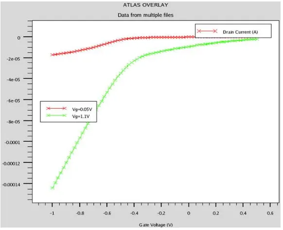
Fig. 1 shows the graph of ID versus VG at VD=0.05V and VD=1.1V for both devices. The threshold voltage value is –0.14724V. This value is still in range ± 12.7% from the nominal value. The nominal value of threshold voltage for PMOS device is -0.15V ITRS, (2007). At VTH=-0.14724V, the values of poly sheet resistance and leakage current are 67.29Ω/ and 0.190395 mA/mm respectively.
The results of VTH were analyzed and processed with Taguchi Method to get the optimal design. Then, the optimum values of the process parameter from Taguchi Method were simulated in order to verify the predicted design.
Analysis of effect HALO and S/D implant on Threshold Voltage:
Fig. 1: Graph ID-VG for 45nm PMOS device
Threshold voltage of the 45nm devices belongs to the nominal-the-best quality characteristics. This S/N Ratio is selected to get closer or equal to a given target value, which is also known as the nominal value Naidu, (2008). The S/N Ratio, h can be expressed as (Douglas C. Montgomery, 2005; Ugur Esme, 2009):
(1)
While n is number of tests and Yi the experimental value of the threshold voltage, m is mean and s is variance. By applying Equations (1)-(3), the S/N Ratios (h) for PMOS device was calculated and given in Table 5. The effect of each process parameter on the S/N Ratio at different levels can be separated out because the experimental design is orthogonal. The S/N ratio for each level of the process parameters is summarized in Table 6. In addition, the total mean of the S/N ratio for the 9 experiments is also calculated and listed in Table 6.
Table 5: Mean, Variance and S/N Ratios For PMOS device
Exp. No. Mean Variance S/N Ratio (Mean) S/N Ratio (Nominal-the-Best)
Table 6: S/N Responses For The Threshold Voltage
Symbol Process Parameter S/N Ratio (Nominal-the-Best) Total Mean S/N Max- Min
---Level 1 Level 2 Level 3
A Halo Implant. 30.69 21.56 20.90 24.39 9.79
B S/D Implant. 24.65 26.04 22.47 3.57
C Oxide Growth Temp. 24.57 25.79 22.79 3.00
D Silicide Anneal Temp. 25.67 26.25 21.24 5.01
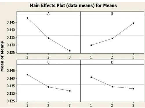
Fig. 2 and Fig. 3 show the S/N ratio and Means graphs of PMOS device respectively. Basically, the larger the S/N ratio, the quality characteristic for the threshold voltage is better Ugur Esme, (2009). The closer the quality characteristic value to the target, the better the product quality will be Naidu, (2008).
Fig. 2: S/N Ratio graph for threshold voltage in PMOS device
Fig. 3: Means graph for threshold voltage in PMOS device
Analysis of Variance (ANOVA):
Table 7: Result of ANOVA for PMOS Device
Symbol Process Parameters Degree of Sum of Mean square F-Value Factor Effect on Factor Effect on
Freedom Square S/N Ratio (%) Mean (%)
A Halo Implantation 2 180 90 35 70 52.21
B S/D Implantation 2 19 10 4 8 25.91
C Oxide Growth Temperature 2 14 7 3 5 14.19
D Silicide Anneal Temperature 2 45 23 9 17 7.69
For PMOS device, halo implantation was found to be the major factor affecting the threshold voltage (70%), whereas silicide anneal temperature was the second ranking factor (17%). The percent effect on S/N ratio of S/D implantation and oxide growth temperature are lower being 8% and 5% respectively. The optimized factors for PMOS device which had been suggested by Taguchi method are shown in Table 8. With all information, it can be clearly said that for the design, S/D implantation was defined as an adjustment factor because it has a small effect on the variance (8%) and large effect on the mean (25.91%). The S/D implantation can be adjusted within 6.55x10¹³
to 6.65x10¹³
atom/cm3
to get the threshold voltage closer to the nominal value.
Table 8: Best Setting of the Process Parameters
Symbol Process Parameters Unit Best Value
A Halo Implantation atom/cm3
3.37x10¹³
B S/D Implantation (as an adjustment factor) atom/cm3
6.60x10¹³
C Oxide Growth Temperature oC 820
D Silicide Anneal Temperature oC 910
From the above parameters as shown in Table 8, the final simulation was performed to verify the accuracy of the Taguchi Method prediction. The results of the final simulation for PMOS device are shown in Table 9.
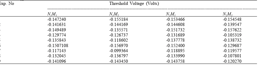
Table 9: Results of the Confirmation Experiment
Threshold Voltage (Volts) S/N Ratio (Mean) S/N Ratio (Nominal- the-best )
---N1M1 N1M2 N2M1 N2M2
-0.141631 -0.144169 -0.144608 -0.139547 -16.9 35.6
The value is exactly same with ITRS prediction Naidu, (2008). In this research, halo implantation has the strongest effect on the response characteristics. The S/N Ratio for PMOS after the optimization approaches is 35.6 dB. This value is within the predicted S/N ratio range of 35.54 to 35.70 dB. These show that Taguchi Method can predict the optimum solution in finding the 45nm PMOS fabrication recipe with appropriate threshold voltage value.
Conclusion:
As conclusion, the optimum solution in achieving the desired transistor was successfully predicted by using Taguchi Method. There are many physical limitations involved as the size gets smaller approaching the molecular or atomic limitations of the substrate and dopant. Threshold voltage (VTH) is the main response in determining whether the device works or not. Poly sheet resistance and leakage current should also be kept as low as possible to increase the speed of the device by shortening the time to accumulate charge in the channel for a transistor to turn on. In this research, Halo Implantation was identified as one of the process parameter that has the strongest effect on the VTH. Whereas the S/D Implantation was identified as an adjustment factor to get the nominal values of threshold voltage for PMOS device closer to -0.150V.
ACKNOWLEDGMENT
The authors would like to thanks to the Ministry of Higher Education (MOHE) for their financial support, Photonic Lab Universiti Kebangsaan Malaysia (UKM) and Universiti Teknikal Malaysia Melaka (UTeM) for the moral support throughout the project.
REFERENCES
Ashok K.Goel et al., 1995. “Optimization of Device Performance Using Semiconductor TCAD Tools”, Silvaco International, Product Description, Silvaco International. http://www.silvaco.com/products/descriptions Belal Ahmed Hamida, 2007. “Optimization of pMOS 65nm Using Taguchi Method”, Master of Science Thesis, Universiti Kebangsaan Malaysia.
Croon, J.A., E. Augendre, S. Decoutere, W. Sansen, H.E. Maes, 2002. “Influence of Doping Profile and Halo Implantation on the Threshold Voltage Mismatch of a 0.13mm CMOS Technology”, ESSDERC.
Douglas, C. Montgomery, 2005. “Design and Analysis of Experiments”, John Wiley & Sons Inc., 6th Edition.
Hani Noorashiqin Abd. Majid, 2007. “Optimization and characterization of 130nm CMOS Transistor design Using TCAD Simulation”, Master of Science Thesis, University of Malaya.
Husam Ahmed Elgomati, 2007. “Characterizing Cobalt Silicide and Gate Dielectric Thickness in 65nm NMOS Device”, Master of Science Thesis, Universiti Kebangsaan Malaysia.
Jiong Guang Su, Shyh-Chyi Wong, Chi-Tsung Huang, 1998. “A study of tilt angle effect on Halo PMOS performance”, Microelectronics and Reliability, 38(9): 0026-2714: 1503-1512.
ITRS, 2007. Report; http://www.itrs.net
Naidu, N.V.R., 2008.“Mathematical model for quality cost optimization, Robotics and Computer-integrated Manufacturing”, Vol.24, Issue 6, 17th
International Conference on Flexible Automation and Intelligent Manufacturing, pp: 811-815.
Ninomiya S., et al., 2009. “Vth Control by Halo Implantation using the SEN's MIND System”, The 9th International Workshop on Junction Technology, pp: 100-103.
Sze, S.M., 1986. “Semiconductor Devices: Physics and Technology”, John Wiley & Sons Inc, 2nd
Edition. Ugur Esme, 2009. “Application of Taguchi Method for the Optimization of Resistance Spot Welding Process”, The Arabian Journal for Science and Engineering, 34: 2B.