UNIVERSITI TEKNIKAL MALAYSIA MELAKA
A SINGLE POLE DOUBLE THROW (SPDT) SWITCH FOR
WIRELESS DATA COMMUNICATION
This report submitted in accordance with requirement of the Universiti Teknikal Malaysia Melaka (UTeM) for the Bachelor Degree of Engineering Technology
(Electronic Telecommunication) (Hons.)
by
HANIS ZAHIRAH BINTI KATMIN
B071110255
910206105522
UNIVERSITI TEKNIKAL MALAYSIA MELAKA
BORANG PENGESAHAN STATUS LAPORAN PROJEK SARJANA MUDA
TAJUK: A Single-Pole Double Throw (SPDT) Switch for Wireless Data Communication
SESI PENGAJIAN: 2014/15 Semester 2
Saya HANIS ZAHIRAH BINTI KATMIN
mengaku membenarkan Laporan PSM ini disimpan di Perpustakaan Universiti Teknikal Malaysia Melaka (UTeM) dengan syarat-syarat kegunaan seperti berikut: 1. Laporan PSM adalah hak milik Universiti Teknikal Malaysia Melaka dan penulis. 2. Perpustakaan Universiti Teknikal Malaysia Melaka dibenarkan membuat salinan
untuk tujuan pengajian sahaja dengan izin penulis.
3. Perpustakaan dibenarkan membuat salinan laporan PSM ini sebagai bahan pertukaran antara institusi pengajian tinggi. atau kepentingan Malaysia sebagaimana yang termaktub dalam AKTA RAHSIA RASMI 1972)
(Mengandungi maklumat TERHAD yang telah ditentukan oleh organisasi/badan di mana penyelidikan dijalankan)
Alamat Tetap:
FAKULTI TEKNOLOGI KEJURUTERAAN
PENGKELASAN LAPORAN PSM SEBAGAI SULIT/TERHAD LAPORAN PROJEK SARJANA MUDA TEKNOLOGI KEJURUTERAAN ELEKTRONIK (TELEKOMUNIKASI): HANIS ZAHIRAH BINTI KATMIN
Sukacita dimaklumkan bahawa Laporan PSM yang tersebut di atas bertajuk
“A Single-Pole Double Throw (SPDT) Switch for Wireless Data
Communication” mohon dikelaskan sebagai *SULIT / TERHAD untuk
tempoh LIMA (5) tahun dari tarikh surat ini.
2. Hal ini adalah kerana IANYA MERUPAKAN PROJEK YANG DITAJA OLEH SYARIKAT LUAR DAN HASIL KAJIANNYA ADALAH SULIT.
Sekian dimaklumkan. Terima kasih.
Yang benar,
________________
Tandatangan dan Cop Penyelia
* Potong yang tidak berkenaan
NOTA: BORANG INI HANYA DIISI JIKA DIKLASIFIKASIKAN SEBAGAI
SULIT DAN TERHAD. JIKA LAPORAN DIKELASKAN SEBAGAI TIDAK
TERHAD, MAKA BORANG INI TIDAK PERLU DISERTAKAN DALAM
DECLARATION
I hereby, declared this report entitled “PSM Title” is the results of my own research except as cited in references.
Signature : ……….
Author’s Name : HANIS ZAHIRAH BINTI KATMIN Date : 15TH DECEMBER 2014
APPROVAL
This report is submitted to the Faculty of Engineering Technology of UTeM as a partial fulfillment of the requirements for the degree of Bachelor of Engineering Technology (Electronic Telecommunication) (Hons.). The member of the supervisory is as follow:
……… (Project Supervisor)
ABSTRAK
Rekaan topologi bagi suis Satu Kutub Dua Arah (SPDT) untuk komunikasi data tanpa wayar telah dihasilkan. Contoh bagi aplikasi yang telah di gunakan adalah pensuisan Time Division Duplex (TDD) seperti di dalam teknologi 4G dan 3G. Kadar pengasingan yang tinggi dan kadar kehilangan sisipan yang rendah akan menghasilkan proses yang terbaik. Rekaan PIN diod secara siri-pirau dan operasi simulasi litar pada 0.5 GHz hingga 3.5 GHz menggunakan perisian Advanced Design System (ADS). Pengasingan, kehilangan kemasukan dan kehilangan pengembalian pada suis SPDT telah di analisis menggunakan S-parameter. Berdasarkan penambahbaikan proses yang mengambil parameter tertentu, topologi gerak siri dan jalur-mikro akan meningkatkan kadar pengasingan.
ABSTRACT
A design a topology of Single Pole Double Throw (SPDT) Switch in Wireless Data Communication is presented. The example of application that implements is Time Division Duplex (TDD) switching such as in 4G and 3G technologies. A high isolation and low insertion loss will make the better performance. The design of the series-shunt PIN diode and the circuit’s simulation operation in 0.5 GHz to 3.5 GHz with Advanced Design System (ADS) software. The isolation, insertion loss and return loss of SPDT switches are analyses by using S-parameter. Regarding to improve the performance that consider parameters, the series-shunt switch topology and the type of transmission lines which increase the isolation.
DEDICATION
To my beloved parents
ACKNOWLEDGEMENT
First, I am highly thankful and indebted to Allah S.A.W for providing me a peace of mind, ability, opportunity and will to complete this work. I would like to thank the following people for their support and assistance with this project’s research. The Special thanks to my beloved parents and my special person that give courage to me until this project completed. Deepest gratitude are also due to my supportive supervisor, Mr. Win Adiyansyah Indra and my co-supervisor, Mrs. Eliyana binti Ruslan, without whose knowledge and assistance this project would not have been successful. Not forgetting to my RF and microwave’s lecturer, Mr.Faizal bin Zulkifli, who willingness to spend his time to solve my project’s problem and gave suggestion for my project. Furthermore, I would like to acknowledge with much appreciation of his criticism during my project’s presentation, Mr. Md Ashadi bin Md Johari, that give inspiration and advised for may Final Year’s Project (PSM). Finally, an honourable mention goes to my fellow friends for their understanding on me in completing this project. Without helps of the particular that mentioned above, I would face many difficulties to complete my project.
TABLE OF CONTENT
2.3 Wireless Data Communication 10
2.3.1 Wi-Fi 10
2.3.2 Cellular Data 11
2.3.3 Mobile Satellite Communication 11
2.3.4 Wireless Sensor Networks 11
2.4 Series-Shunt Switch 12
2.5 S-parameter (Scattering Parameter) 13
CHAPTER 3: METHODOLOGY 15
3.1 Project Flow 17
3.2 Design Process 17
CHAPTER 4: RESULT & DISCUSSION 19
4.1 Topology of the schematic 19
4.1.1 Series PIN diode 21
4.1.2 Quarter-wavelength Transmission Line 22
CHAPTER 5: CONCLUSION & FUTURE WORKS 24
5.1 Summary of Project 24
5.2 Achievement of Research Objectives 24
5.3 Problems Faced During Research 24
5.4 Suggestion for Future Work 25
REFERENCES 26
APPENDICES
LIST OF TABLES
4.1 Measurement data to performance for RF switch with quarter-wavelength.
21
LIST OF FIGURES
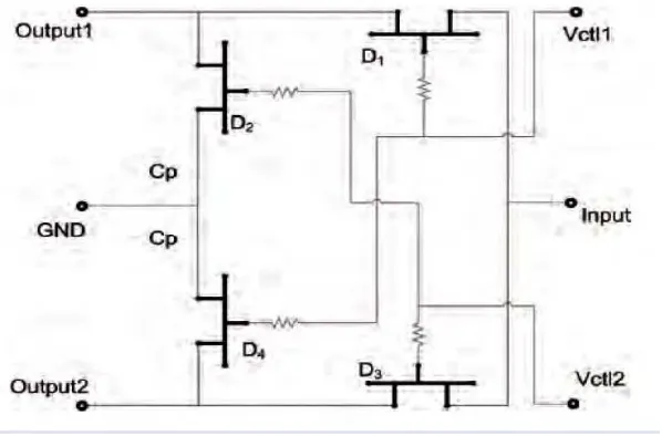
2.1 Typical SPDT switch circuit (Yang and Cory, 2010) 6
2.2 Layer of PIN diode. 8
2.3 Simplified T/R Switch (Yang and Cory, 2010) 8
2.4a Series SPDT switch (CECS, n.d) 13
2.4b Shunt SPDT switch (CECS, n.d) 13
2.5 The two-port network (ECE, 2011) 13
3.1 The flow chart of the project 16
4.1 The schematic design of shunt-series SPDT switch 19
4.2 The simulation data at transmit mode 20
4.3 The simulation data at receive mode 20
4.4 The parameter’s value of PIN diode 22
4.5 The setting parameter’s value 23
4.6 The microstrip line’s parameter 23
LIST OF ABBREVIATIONS, SYMBOLS AND
DECT - Digital Enhanced Cordless Telecommunication Rs - Series resistance
Cj - Junction capacitance
WiMAX - Worldwide Interoperability for Microwave Access CDMA - Code Division Multiple Access
ADS - Advanced Design System DUT - device under test
MEMS - micro-electromechanical system LNA - low-noise amplifier
This chapter covers the introduction of the project, backgrounds study regarding the project topics, problem statements of the projects, project objectives, project scope, project significance and conclusion of all part in project introduction.
1.1 Background
Single-Pole Double Throw (SPDT) switch is commonly used in RF and microwave transceiver system for perform Time Division Duplex (TDD) switching for transmit and receive operation. It diversity receive technique are mandatory to increase data rates in emerging mobile phone radius. TDD that is performs in Long-Term Evolution (LTE) in 4G technologies, Digital Enhanced Cordless Telecommunication (DECT), TD SCDMA (3G mobile telephony air interface, TD-CDMA (indoor mobile telecommunication), PACTOR (radio modulation mode used by amateur radio operator, marine radio station and radio station in isolate area) and WiMAX.
The high demand and rapid pace of the development of spectrally efficient, and now energy efficient, wireless communication systems that are capable of supporting a diverse range of applications needing high bandwidths and differentiated quality of service has created a strong and vibrant global market for communication engineers needing specialist skills in wireless systems. These kinds of technologies lead an inventors or society to upgrade the performance of speed up due to population that cause increase of communication usage and customer demands.
INTRODUCTION
CHAPTER 1
On top of that, this project’s research discuss about better performance, good isolation and less insertion loss based on SPDT switch that practical in wireless data communication system. There are few methods or techniques to obtain the desired results. The first technique is by through material and fabrication process of switch elements. Secondly, the resonated switch element with inductor and capacitors. Last but not least, by switch configuration. In this project, the third method is using design series-shunt switch.
However, this project must consider a few elements in term of cost, time and current consumption. Although the first technique will produce good performance but it will need a lot of cost and complex process. In second’s technique, it will limit in narrowband isolation due to single resonant tank circuit. Based from the constraints above, this project finally found suitable method which is switch configuration.
1.2 Problem Statement
Most of the engineer nowadays tried really hard to make the improvement. This project needed to improve the performance of this device, for better performance and based the parameters result such as isolation, insertion loss and return loss in wireless data communication. As a solution, this project designed the better topology, series-shunt switch connection and series PIN diode. However, it is due on cost need to spend in complex process. Besides that, time is the one of the constraints towards this project. A lot of effort such deep research about this project necessary to make better improvement and performance.
1.3 Objectives
The objectives of this project is to design the device which able to makes an improvement for better performance, high isolation, lower insertion loss and lower
return loss. Moreover, this project will analysis and understand the standard discrete PIN diode that used in switching applications.
1.4 Scope
The scope of this project is limited to the following items so that it will be focused based on the stated objectives.
(a) This design focus on the basic RF switch which is SPDT switch.
(b) The different types of SPDT switch for wireless data communication that result will be in different desired.
(c) This project gives opportunity to analysis PIN diode as a switch.
(d) Design and simulate the data from SPDT switch topology in Advance Design System (ADS) software.
(e) An analyze the RF switch topology in ADS software.
1.5 Project Significance
The impact of the development of wireless data communication will give opportunity to society besides it will contribute in economic. In additional, the improvement of technologies due to increase of society will generates innovation, because it promotes and facilitates the invention and production of new services, products or processes.
Moreover, it will give chance to human to communicate without boundaries everywhere and every time that they need. These technologies also gives everyone a chance to upgrade their livelihoods by expanding and strengthening social networks such as increase people’s ability to deal with emergencies, cut down travel costs, maximize the outcomes of necessary journeys, increase temporal accessibility and amplify efficiency of activities.
1.6 Conclusion
In the nutshell, this project that follow of the objectives will obtain the desire results lead to the improvement in SPDT for wireless data communication due to the customers demand. They also cover the knowledge of the basic RF switch and the parameters that involved in this project.
This chapter is discusses the information and theory relates to this project also the overview of major components involved. Factors that should be consider while developing this project also will be cover. The literature review will start with reviewing the RF switches types, classification and functions. Furthermore, the RF switch is designed based on type, function and requirements of wireless system. The design that has been chosen will be stated at the end of this chapter.
2.1 RF Switch
An RF (which stand for Radio Frequency) and microwave switch is a device to route high frequency signal through transmission paths. RF and microwave switches are used extensively in microwave test systems for signal routing between instruments and devices under test (DUT). Incorporating a switch into a switch matrix system enables to route signals from multiple instruments to signal or multiple DUTs. This allows multiple tests to be performed with the same setup, eliminating the need for frequent connects and disconnects. The entire testing process can be automated, increasing the throughput in high-volume production environments.
Pat Hindle (2010a) states RF and microwave switches classified into the two main categories of electromechanical and solid-state switches. The electromechanical switches not used widely in RF and microwave applications since the PIN diode had been practice and develop, they are making some new invent to being applied in the form of electromes in certain applications in the form of
micro-LITERATURE REVIEW
CHAPTER 2
electromechanical systems (MEMS) devices. Solid-state switches are typically more reliable and exhibit longer lifetime than electromechanical switches, besides faster in switching times. However, solid-state switches typically have higher intrinsic ON resistance and more harmonic distortion than mechanical switches.
RF and microwave switches come in different configurations providing the flexibility to create complex matrices and automated test systems for many different applications. The one of the typical configuration switch is SPDT. Shairi et al. (2013) explained the key parameter in SPDT switch design is the requirements of high isolation between transmitter and receiver that cause distorting receiver’s active circuits especially low noise amplifier (LNA).
Ricky and Jay (2010), in order to integrate these applications into getting smaller physical volume of the mobile devices, each functional block has to be scaled in reduce size. In today’s digital communication system systems, switches are playing an important role in a variety of functions, such as transmit/receive (T/R) switching and power control, which affect the overall terminal performance.
Figure 2.1: Typical SPDT switch circuit (Yang and Cory,2010)
This RF and microwave switches must consider the certain parameters which are isolation, insertion loss and return loss. The insertion loss is the loss of the signal power resulting from the insertion of a device in a transmission line or optical fibre and usually in decibels (dB). The insertion loss can be express by formula below;
10 log10 ��
��
In telecommunication, return loss is the loss of the signal power resulting from the reflection caused at a discontinuity in a transmission line or optical fibre. This discontinuity can be mismatch with the terminating load or with device inserted in the line.
RL (dB) = 10 log10 ����
Isolation is the degree of attenuation from an unwanted signal detected at the port of interest. Isolation becomes more important at higher frequencies. High isolation reduces the influence of signals from other channels, sustains the integrity of the measured signal, and reduces system measurement uncertainties. In instance, a switch matrix may need to route a signal to a spectrum analyzer for measurement at -70 dBm and to simultaneously route another signal at +20 dBm. In this case, switches with high isolation, 90 dB or more, will keep the measurement integrity of the low-power signal.
On top of that, there are several techniques that improve isolation. Shairi et al. (2009) state multiple connections of shunt PIN diodes and combination of series-shunt PIN diode. However, it will increase current consumption and overall size circuit. Other than that, Tsukahara et al. (2008) where a technique using shunt stub resonators controlled by FET implement for isolation improvement of SPDT MMIC switch.
2.2 PIN Diode
A PIN diode is a current controlled resistor at radio and microwave frequencies. Basically, it is a silicon semiconductor diode in which a high-resistivity intrinsic I-region is sandwiched between a P-type and N-type region.
Figure 2.2: Layer of PIN diode.
Pat Hindle (2010b) found a PIN diode brightly in a very high power and high frequency applications with low insertion loss and better power handling capabilities when compared to most IC FET switches. The PIN diode operates as a variable resistor at RF and microwave frequencies. It is ON resistance varies from less than 1 Ω (ON) to more than 10 kΩ (OFF) depending on the bias. One limitation of a PIN diode switch is its lower frequency limit of a few kHz to about a MHz depending on the thickness of intrinsic (I) region.
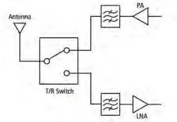
A PIN diode based T/R switch is a practical design for base station and infrastructure applications. Figure 2.3 illustrates how a SPDT switch can be used to connect a transmitter and a receiver to a common single antenna in a single duplex system.
Figure 2.3: Simplified T/R Switch (Yang and Cory, 2010)
Shairi (2010) mentioned PIN diode is beneficial for leveling and amplitude modulating a RF signal. When the control current is switched “on” and “off” or in discrete steps, the device is practically for switching pulse modulating, attenuating and phase shifting of a RF signal. In additional, the PIN’s small size, weight, high switching speed and minimized parasitic elements make it ideally suited for use in miniature, broadband RF signal control components.
At RF, a PIN diode acts as either a small valued capacitor or as a variable resistor, depending on the DC bias applied to the diode. If the diode is reverse biased at DC, at RF it behaves as a very small value capacitor with the capacitance of approximately 1 pF. Through RF can get through a 1 pF capacitor, the amount that gets through is quite small. If the leakage through 1 pF is a problem, several diodes can be strung in series, reducing the capacitances and thus the residual leakage, thus, for RF, the PIN diodes acts as an open switch if it is reverse biased with DC. Even though the alternating RF current superimposed on the DC may occasionally forward bias the diode, the slow response time caused by the extra “I” layer prevents it from turning on.
When PIN diode in forward biased state at DC, for RF it behaves like a resistor. The RF resistance is inversely proportional to the forward DC bias current. The resistance might be as high at 10,000 Ω for very small forward currents, and as low as 0.1 Ω if the forward DC bias current is 100 mA. Each type of diode has a different resistance versus forward bias characteristic. If the forward current through the diode is near the maximum the diode is designed for, it typically has an RF resistance of only 0.1 Ω, and thus acts as a closed switch. Thus, for RF, the PIN diode acts as a closed switch if it is forward biased with the near maximum DC bias current. Even though the alternating RF current superimposed on the DC may occasionally reverse bias the diode, the slow response time caused by extra “I” layer prevents it from turning off.
If both DC and RF to a PIN diode apply at the same time, the PIN diode can use as an RF switch. Reverse biasing the diode at DC turns the switch off, and forward biasing the diode at DC turns on the switch. The resulting “solid state switch” has a switching time much faster than any mechanical switch or relay.
Pat Hindle (2010c), a PIN diode switches can consists of a combination of series and/ or shunt diodes depending on the circuit requirements. Series PIN diode can function within a wide bandwidth limited by the biasing inductors and DC blocking capacitors, while shunt diodes features high isolation relatively independent of frequency. Circuit designers often use transmission lines to create series lumped inductance to achieve a low pass filter effect, which enables to switch to work up to the desired frequency. Shunt diode switches has limited bandwidth appear from the quarter wavelength transmission lines’ uses between the common junction and each