DOI: 10.12928/TELKOMNIKA.v13i3.1426 813
Study and Design of 40 nW CMOS Temperature Sensor
for Space Applications
Abhishek Pandey*, Vijay Nath
VLSI Design Lab, Birla Institute of Technology Mesra, Ranchi Jharkhand India 835215 *Corresponding author, e-mail: [email protected]
Abstract
In the present study, a novel CMOS temperature sensor based on sub-threshold MOS operation has been presented, which is designed for space and satellite applications. The proposed CMOS temperature sensor is enunciated a good linearity between temperatures range from -60OC to 150OC with inaccuracy of -1.8OC. This circuit is operated at supply 1V and static power consumption 40nW at 150OC is achieved. The circuit utilizes the temperature dependency of threshold voltage of MOSFET, which gives two types of voltage in output, first voltage proportional to absolute temperature (PTAT) and second,
negative temperature coefficient (NTC). The sensitivity of both PTAT and NTC is 0.16390mV/oC and
0.17607mV/oC respectively between the specified range -60 OC to 150 OC. This circuit is designed & simulated using Cadence analog & digital design tools UMC90nm CMOS technology. The layout area of the circuit is 17.213μm ൈ 6.655μm.
.
Keywords: CMOS; complementary metal oxide semiconductor, temperature sensor, PTAT, proportional to absolute temperature, NTC, negative temperature coefficient, low power
Copyright © 2015 Universitas Ahmad Dahlan. All rights reserved.
1. Introduction
Temperature is very important physical quantity in our daily life. It is applied in various fields such as industrial, medical, space and defense etc. In aircraft, the temperature monitoring play important role in fuel consumption, environmental cooling systems, oil in hydraulic, lubricating system, fluid in coolant, heating systems and avionics systems [1]. Today it’s heavy demand of the CMOS temperature sensor due to use in thermal management. The advantage of CMOS based efficient temperature sensor is monitoring the steady increase of heat dissipation in different system. It is required to track the process temperature and regulate its cooling fan.
Temperature sensors are commonly divided into two type (a): conventional sensors (b): smart sensors. The conventional temperature sensors are having numerous drawbacks when compared to the smart temperature sensors specially manufactured in CMOS technology consuming more power due to the larger area, less accurate and non-linearity [2]. The smart temperature sensor can directly communicate with a microcontroller / microprocessor in a standard digital format, result reducing the complexity and enhance the response of the system. CMOS Smart temperature sensor circuit consist temperature cell circuit, its signal conditioning circuit and Analog to digital converter [3]. In silicon based MOSFET there is much property which depends on temperature. On the basis of literature report, the smart temperature sensor further designed in to (i) Parasitic BJT based temperature sensor, (ii) delay-Inverter based temperature sensor, (iii) Threshold voltage temperature sensor.
CMOS technology is used to realize parasitic BJTs which based on lateral PNP transistors have been realized achieve challenges related to temperature sensing like less accuracy, consuming more power, and occupying a large area. Now CMOS technology is growing and semiconductor industry adopted this technology frequently due to low fabrication cost and easy fabrication process. The temperature-sensing accuracy of BJTs is limited by the effect of their saturation current (IS), which can lead to errors of a few degrees. But this error can
conventional temperature sensor. But there are use at least two PNP transistors, result increases the size of the chip.
Propagation delay-based temperature sensor is designed on the concept of the propagation delay of inverters. Delay line based temperature sensor consumes less power than a parasitic BJTs temperature sensor. The delay is a function of temperature for this type of sensor. For the digitization we need time to digital converter. Subsequently, the output pulse is fed to the input of a cyclic Time-to-Digital Converter (TDC) to generate the corresponding digital [8-10]. The same technique can be also be implemented in another way by measuring the variation in frequency of oscillation caused by variation in temperature. The frequency is inversely proportional to temperature because the decrease in the mobility is the dominant feature [11-12]. Both of these kinds of sensors require a larger chip area and produces difficulty in attaining linearity for the higher range.
To overcome the limitation of CMOS technologies in various temperature sensors (as discussed above), we opted threshold voltage, temperature sensor with for the application in the avionic system, owing to good accuracy with minimum power consumption. The temperature sensors based on the threshold voltage of MOSFETs are known for their lower power consumption and smaller die area [13-16]. The voltage or current across MOSFETs is always varies with the temperature, but the challenge is designing these types of sensors is accuracy. Because linearize this variation is a difficult task. This task is accomplished by proper selection of circuit architecture and adjusting the W/L ratio of the transistors used so that the non-linearity can be reduced.
The rest of this paper has been organized as follows. The characteristic of MOSFET operating in Basic Principle of MOSFET based temperature sensor is given in Section II. Section III describes the methodology and architecture of the proposed temperature sensor circuit. The simulation result and discussion has been summarized in Section IV. Finally, the conclusion of the overall paper is illustrated in Section V.
2. Basic Principle
The small signal analysis the square law of model is not longer holds true. Therefore, we cannot neglect the second order effect. The second order effect will cause temperature nonlinearity.
On chip thermal sensing demonstrates several degree Celsius temperature errors [16] due to nonlinearity. For short channel devices, the effect of velocity saturation and mobility degradation on the drain current in the saturation region [17-20] is defined as:
DSn Tn GSn V V
V
0
sat Tn GSn ox n D lV V V l w c I 2 1 2 (1) Where, GSnV
= Gate Source voltageV
DSn= Drain Source voltageV
Tn=Threshold voltageI
D=drain current of MOS transistor
n= mobility of N-type materialc
ox= oxide capacitancew= channel width of MOS transistor
l
= channel length of MOS transistorV
sat=
nE =s
m
/
10
7 constant saturation velocity
= fitting parameter
7 1
/10 toxV
Where Vt Vto
2F VSB 2F
(2)And,
ox F SUB si F
FB SB
t to
c N q V
V V
V ( 0) 2 2 2 (3)
Where,
Bulk Threshold Voltage,
F
Strong Inversion Surface Potential,V
FB=Flat Band Voltage,Q
SS
Oxide-charge=qN
SS,
k
Boltzmann’s constant, T Temperature (K),
i
n
Intrinsic carrier concentration.
T V
T0 k
T T0
V (4)
From Equation (4) it is proved that Threshold voltage decreases with increasing temperature hence the drain current increase. Therefore the drain current increases. This is the reverse dependence.
In MOS device mobility is important parameters that are predominantly sensitive to temperature. Theoretically Mobility of the carrier in the channel can be defined as [23-24].
k
T T T T
0 0).
(
(5)\
Where,
0
T
= Reference temperature T = Absolute temperatureWhere k = constant value between -1.2 and 2.42 around room temperature, causing the mobility decrease by about half a percent per degree. The expression for the channel mobility can be further complicated by introducing velocity saturation and mobility degradation. This word means that the mobility at the reference temperature
(
T
0)
depends upon the bias voltage and the threshold voltage. As temperature increases, the carrier mobility decreases and resulting drain current decreases. This is the normal dependence.Threshold Voltage variation with the temperature
3. Proposed Circuit
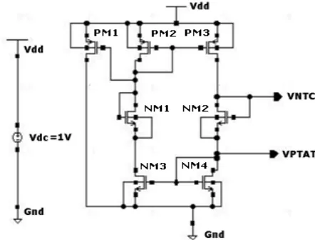
The schematic diagram of temperature sensor circuit is shown in Figure 1. The proposed circuit is made by 4 NMOS and 3 PMOS transistors. Since in NMOS transistor, mobility is higher than the PMOS, therefore it is working as better switch and PMOS work as better load. The load is working as a resistance and the resistance is directly related to temperature. The both output PTAT and NTC voltages have been extracted. In the proposed design the transistors PM1, PM2 and PM3 act as active load, which form the current mirror through transistors PM3, PM2 and PM1. From equation (6) it is clear that the aspect ratio of PM2 and PM3 decided the nature of temperature vs voltage. Since PM2 and PM3 form current mirror therefore the aspect ratio of PM2 and PM3 should be same. This same current mirror helps in obtaining the voltage due to difference in current flow. The W/L ratios of the transistors configured as active resistors are also suitably adjusted for linearization of the output voltages.
Figure 1. Circuit diagram of CMOS Temperature Sensor Cell T N P P T
PTAT V kV
V 1 12 23 23 2 3
1
(6) T N P N TNTC V k V
V 2 12 23 12 3 2
1
(7) Where 3 3 2 2 23 P P P P P
L
W
L
W
Where 2 2 1 1 12 N N N N N L W L W
4. Simulation Result & Discussion
The proposed temperature sensor circuit has been simulated in Analog Design Environment of Cadence using UMC90nm library. This circuit uses a 1V supply. The PTAT and NTC characteristics have been extracted from the circuit. The proposed circuit has been designed for sensing temperature from -60oC to 150oC and shows a good linearity between these ranges. The PTAT voltage gives an output voltage of 384.51987mV at -60oC and 418.93929 at 150oC. The sensitivity for VPTAT is 0.16390mV/
o
C. The NTC voltage shows an output voltage of 675.44597mV to 639.35949mV for the temperature range of -60oC to 150oC respectively with a sensitivity of 0.17607mV/oC. Both VPTAT and VNTC curves has been shown in
Figure 2(a).
The maximum deviation from actual value at any given temperature in between the specified range of the sensor is known as inaccuracy of any temperature sensor. The inaccuracy of NTC voltage in a specified range of the proposed sensor is -1.8oC respectively. The error of NTC shows better than the PTAT. The error curves for VNTC are given in Figure
2(b).
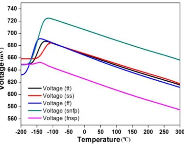
two-letter, because two types of MOSFET used in CMOS technology: namely NMOS for n-channel and PMOS for p-channel. On behalf of the mobility of MOS transistor there are three type corner rules: (i) typical (t), (ii) fast (f) and (iii) slow(s), which used fast and slow for carrier mobility that is higher and lower than normal, respectively. There are five process corners [25] are involved to simulated my proposed circuit namely: (i) typical-typical (tt), (ii) fast-fast (ff), (iii) slow-slow (ss), (iv) fast-slow (fnsp), and (v) slow-fast (snfp). The (i) to (iii) is called even corners because both types of devices affected same, hence there are no adverse effect of the logical correctness of the circuit. This means the devices can operate at slower or faster clock frequencies. The last two process corners are called as skewed corner and come to concern corners. That is why in the MOSFET, NMOS will switch much faster than the PMOS. This represents imbalanced switching can cause one edge of the output to have a much less slew than the other edge. The Figure 3(a) & Figure 3(b) shows the simulated result at different process corner of PTAT and NTC respectively.
Figure 2(a). Output Voltage of Sensor with variation of Temperature
Figure 2(b). VNTC Error of temperature cell
Figure 3(a). Temperature vs Voltage graph at different process corner in UMC 90nm technology of VPTAT CMOS Temperature
Sensor
Figure 3(b).Temperature vs Voltage graph at different process corner in UMC 90nm technology of VNTC CMOS Temperature
Sensor
Since power consumption of any CMOS circuit increases with increasing temperature. The circuit draws 40nA current from the circuit, which is shown in Figure 4. Therefore the overall resultant power dissipation of the proposed sensor is 40nW at 150oC.
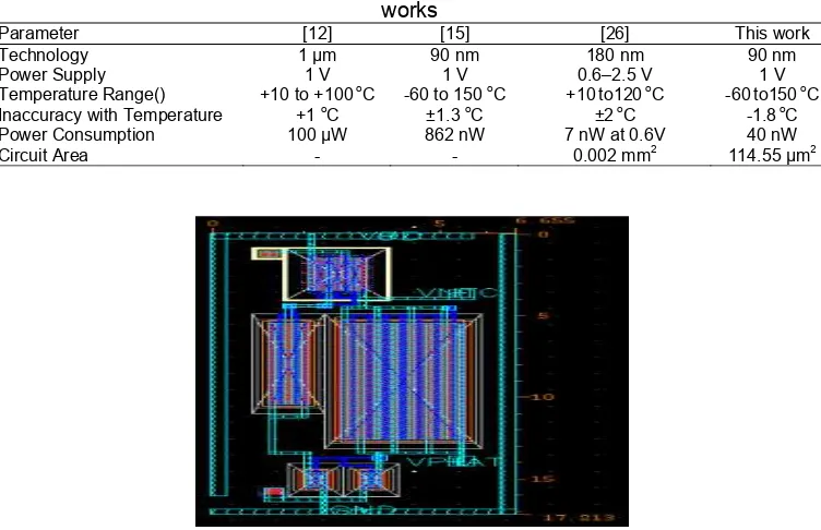
The layout of proposed circuit is shown in Figure 5. The layout area of the cell is 17.213μm ൈ6.655μm. The designed layout of the cell is finally checked with DRC, it is fully error free and fully matched with LVS.
VNTC from the designed sensor is chosen for comparison as it produces better result than VPTAT.
From the table it can be seen that the power dissipation and inaccuracy is better than other result, while the temperature range is quite large. The inaccuracy increases with range. But, the proposed design maintains the inaccuracy in check, well within -1.8oC.
Figure 4. Drawn current from power supply of CMOS Temperature Sensor Cell
Table 1. Performance Summary & Comparison of proposed temperature sensor with recent works
Parameter [12] [15] [26] This work
Technology 1 µm 90 nm 180 nm 90 nm Power Supply 1 V 1 V 0.6–2.5 V 1 V Temperature Range() +10 to +100oC -60 to 150 oC +10 to120oC -60to150 oC Inaccuracy with Temperature +1 oC ±1.3 oC ±2oC -1.8 oC Power Consumption 100 µW 862 nW 7 nW at 0.6V 40 nW Circuit Area - - 0.002 mm2 114.55 µm2
Figure 5. Layout of Proposed Temperature Sensor Cell
5. Conclusion
References
[1] A Pandey, D Yadav, R Singh, Vijay Nath. Design of ultra low power CMOS temperature sensor for space application. IJAREEIE. 2013; 2(8): 4117-4125.
[2] Martinez Brito, Juan Pablo, Aliain Rabacijs. CMOS Smart Temperature sensor for RFID application.
26th Symposium on Integrated Circuits and Systems Design (SBCCI).Curitiba. 2013:1-6.
[3] Bakker A, Huijsing J. Micropower CMOS temperature sensor with digital output. IEEE Journal Solid State Circuits. 1996: 933-937.
[4] Andre L Aita, Michiel AP Pertijs, et al. Low Power CMOS Smart Temperature Sensor with a batch-calibrated of inaccuracy of ±0.25O C (±3σ) from -70 O C to 130O C. IEEE Sensors Journal. 2013; 13(5): 1840-1848.
[5] MAP Pertijs, KAA Golam Chowdhury, A Hassibi. An On-chip Temperature sensor with a self-Discharging Diode in 32-nm SOI CMOS. IEEE transactions on circuits and systems. 2012; 59(9): 568-572.
[6] MAP Pertijs, KAA Makinwa, JH Huijsing. A CMOS smart temperature sensor with 3σ inaccuracy of ±0.1OC from -55OC to 125 OC. IEEE J. Solid-State Circuits. 2005; 40(12): 2805-2815.
[7] Kamran Souri, et al. A CMOS Temperature Sensor with a Voltage-Calibrated Inaccuracy of ±0.15O C (3σ) From 55 O C to 125 O C. IEEE Journal of Solid-State Circuits. 2013; 48(1): 292-301.
[8] P Chen, CC Chen, CC Tsai, WF Lu. A time-to-digital converter-based CMOS smart temperature sensor. IEEE J. Solid-State Circuits. 2005; 40(4): 1642-1648.
[9] P Chen, CC Chen, TK Chen, SW Chen. A time domain mixed-mode temperature sensor with digital set-point programming. IEEE Custom Integration. Circuits Conference. San Jose. 2006: 821-824. [10] K Woo, et al. Dual-DLL-based CMOS all-digital temperature sensor for microprocessor thermal
monitoring. IEEE International conference Solid-State Circuits Conference - Digest of Technical Papers, ISSCC. San Francisco, CA. 2009: 68-69.
[11] Kisso Kim, et al. 366Ks/s 1.09-nJ 0.0013mm2 Frequency to Digital Converter based CMOS Temperature Sensor Utilizing Multiphase Clock. IEEE Transactions on Very Large Scale Integration (VLSI). 2012; 21(10):1950-1954.
[12] Sewook Hwang, Jabeom Koo, et al. A 0.008 mm2 500µW 469 kS/s Frequency-to-Digital Converter Based CMOS Temperature Sensor with Process Variation Compensation. IEEE Transactions on Circuits and Systems Journal. 2013; 60(9): 2241-2248.
[13] V Szekely, Cs Marta, Zs Kohari, M Rencz. CMOS Sensors for On-Line Thermal Monitoring of VLSI Circuits. IEEE Trans. Very Large Scale Integration Systems. 1997; 5(3): 270-276.
[14] M Sasaki, M Ikeda, K Asada. A Temperature Sensor with an Inaccuracy of -1/+0.8°C using 90nm 1-V CMOS for Online Thermal Monitoring of VLSI Circuits. IEEE Trans. Semiconductor Manufacturing. 2008; 21(2): 201-208.
[15] Ueno K, Asai T, Amemiya Y. Low-power temperature-to-frequency converter consisting of subthreshold CMOS circuits for integrated smart temperature sensors. Sensors and Actuators A Physical. 2011; 165: 132-137.
[16] Subhra Chakraborty, Abhishek Pandey, Vijay Nath. A CMOS Temperature Sensor with 60oC to 150oC Sensing Range and ±1.3oC Inaccuracy. IEEE International conference on innovations in information embedded and communication systems-2015 (ICIIECS). Coimbatore. 2015.
[17] Basab Datta. On Chip thermal sensing in deep submicron CMOS. Masters Theses. Amherst: University of Massachusetts; 2007.
[18] Phillip E Allen, Douglas R Holberg. CMOS analog circuit design. 3rd Edition. Oxford: Oxford University press. 2004: 72-159.
[19] Behazad Razavi Design of Analog CMOS Integrated circuits. New York: Tata McGraw-Hill Publishing Company Limited. 2002.
[20] DA Pucknell, Kamran Eshraghian. Basic VLSI Design. 3rd Edition. New Delhi: Prentice-Hall of India Private Limited. 2008.
[21] V Nath, LK Singh, KS Yadav. Design and Development of CMOS Bandgap Voltage Reference Circuit in VLSI. International Journal of Systemics, Cybernetics and Informatics. 2007; 2: 71-75.
[22] Vijay Nath, KS Yadav, LK Singh. Modeling, Simulation and Layout Design of CMOS Signal Conditioning Circuit with M/NEMS Sensors in VLSI. 16th National Seminar on Physics & Technology of Sensors (NSPTS16) organized by Department of Physics, University of Lucknow, India. 2011.
[23] J Altet, et al. Sensing temperature in CMOS circuits for thermal testing. Proceeding of 22nd IEEE VLSI test symposium. 2004: 179-184
[24] Eran Socher, Salomon Michel Beer, Yael Neimirovsky. Temperature sensitive of SOI-CMOS transistor for use in uncooled thermal sensing. IEEE transaction on electron devices. 2005;52(12): 2784-2790. [25] Weste Neil HE, Harris David. CMOS VLSI Design: A Circuits and Systems Perspective. 3rd Ed. New
Delhi: Prentice-Hall of India Private Limited. 2005.