i
THE MINIMIZATION OF 5.75 GHZ CHEBYSHEV BAND PASS FILTER
OTHMAN ABDULLATIF JUSSAB
This report is submitted in partial fulfillment of the requirement for the award of Bachelor of Electronic Engineering (Telecommunication Electronic) With
Honours
Faculty of Electronic and Computer Engineering Universiti Teknikal Malaysia Melaka
ii
UNIVERSTI TEKNIKAL MALAYSIA MELAKA
FAKULTI KEJURUTERAAN ELEKTRONIK DAN KEJURUTERAAN KOMPUTER BORANG PENGESAHAN STATUS LAPORAN
PROJEK SARJANA MUDA II
Tajuk Projek : The Minimization of 5.75 GHz Chebyshev Band Pass Filter
Sesi
Pengajian : 1 1 / 1 2
Saya OTHMAN ABDULLATIF JUSSAB
mengaku membenarkan Laporan Projek Sarjana Muda ini disimpan di Perpustakaan dengan syarat-syarat kegunaan seperti berikut:
1. Laporan adalah hakmilik Universiti Teknikal Malaysia Melaka.
2. Perpustakaan dibenarkan membuat salinan untuk tujuan pengajian sahaja.
3. Perpustakaan dibenarkan membuat salinan laporan ini sebagai bahan pertukaran antara institusi pengajian tinggi.
4. Sila tandakan ( √ ) :
SULIT*
*(Mengandungi maklumat yang berdarjah keselamatan atau kepentingan Malaysia seperti yang termaktub di dalam AKTA RAHSIA RASMI 1972)
TERHAD** **(Mengandungi maklumat terhad yang telah ditentukan oleh organisasi/badan di mana penyelidikan dijalankan)
TIDAK TERHAD
Disahkan oleh:
__________________________ ___________________________________
(TANDATANGAN PENULIS) (COP DAN TANDATANGAN PENYELIA)
iii
“I hereby declare that this report is the result of my own work except for quotes as cited in the references.”
Signature : ………..
Author : OTHMAN ABDULLATIF JUSSAB
iv
“I hereby declare that I have read this report and in my opinion this report is sufficient in terms scope and quality the award of Bachelor of Electronic
Engineering (Telecommunication Engineering) With Honours.”
Signature : ……….
Name : PROF. MADYA DR. ABDUL RANI BIN OTHMAN
vi
vii
ACKNOWLEDGEMENT
First, I am highly thankful and indebted to Allah Subhanahu Wata’ala for providing me peace of mind, ability and will to complete this work.
Peace and Rahmah be upon my father Mr. Abdullatif Jussab Saddique who had inspired me to strive for excellence. May Allah bestow him with Al Firdaus. I am grateful to my mother, Mrs. Khairoon, my grandmother Mrs. Hawa and Aunty Safia for their spiritual support and Dua’as. I am also thankful to all my siblings; namely, Asif, Layla, Nasreen, Muzammil, Mukhtar, Nadir, Rubeena, Nadia, Fatma, Juneid, Nabel, Rukhsaar, Naypheen, Ayman, and Nawaf for their caring and dua’a.
I am very grateful to PM. DR. Abdul Rani bin Othman, who has served for a year as my supervisor for my study towards Bachelor Degree. PM. Dr. Abdul Rani provided invaluable guidance and support throughout the work on this thesis. Without his support and patience I would not have completed my degree.
I would like to express my gratitude to the Faculty of Electronic and Computer Engineering (FKEKK) for giving me a chance to take part on a project which is a requirement to fulfilling the bachelor degree where I had gained great experience and knowledge.
viii
ABSTRACT
This project presents the minimization of Chebyshev 9th order band pass filter
ix
ABSTRAK
x
CONTENTS
CHAPTER TITLE PAGES
PROJECT TITLE i
STATUS CONFIRMATION FORM ii
DECLARATION iii
DEDICATION vi ACKNOWLEDGEMENT vii
ABSTRACT viii
ABSTRAK ix
CONTENTS x
LIST OF TABLES xiii
LIST OF FIGURES xiv
LIST OF ABBREVIATIONS xvi
SYMBOLS xvii
LIST OF APPENDIX xix
I INTRODUCTION 1.1 Introduction 1
1.2 Project Objectives 2
1.3 Project Background 2
1.4 Project Scope 3
1.5 Methodology 4
1.6 Thesis Structure 5
xi
2.1 Introduction 6
2.2 Filters 6
2.2.1 Type of Filters 7
2.2.2 Passive Filters 8
2.2.3 Classification of Filters 8
2.2.4 Band Pass Filters 10
2.3 Literature Survey on Miniaturized Band Pass Filter 11
2.4 Filter Designing Methods 13
2.4.1 Image Parameter Method 13
2.4.2 Insertion Loss Method 15
2.5 Low Pass Filter Prototype 16
2.5.1 Butterworth Low Pass Filter Prototype 18 2.5.2 Chebyshev Low Pass Filter Prototype 21
2.6 Scaling and Conversion 24
2.6.1 Scaling 24
2.6.1.1 Impedance Scaling 24 2.6.1.2 Frequency Scaling 24
2.6.2 Conversion 25
2.7 Filter Realization 27
2.7.1 Microstrip Transmission Line 27 2.7.2 Parallel Coupled Band Pass Filter 28
2.7.3 Glass Epoxy (FR-4) 31
2.8 Summary 32
III METHODOLOGY
3.1 Introduction 33
3.2 Project flow 33
3.3 Chebyshev Band Pass Filter Design 36 3.3.1 Chebyshev Low Pass Filter Prototype 36
3.3.1.1 Graphical Method 36
xii
3.3.3 Filter Implementation 41
3.4 Simulation Process 43
3.5 Hardware Fabrication Process 45
3.6 Measurement Process 46
3.7 Summary 46
IV RESULTS AND ANALYSIS
4.1 Introduction 47
4.2 Simulation Results of Conventional 9th Order 47
Band Pass Filter
4.3 Simulation Results of Ω-Type 9th Order Band 55
Pass Filter
4.4 Simulation Results of W-Type 9th Order Band 59
Pass Filter
4.5 Measurement Results 64
4.5.1 Measurement Results of Ω-Type 9th Order 64
Band Pass Filter
4.5.2 Measurement Results of W-Type 9th Order 64 Band Pass Filter
4.5.3 Comparison of Measurement Results 65
4.6 Summary 67
V DISCUSSION AND CONCLUSION
5.1 Introduction 68
5.2 Discussion 68
5.3 Recommendation 69
5.4 Conclusion 70
REFERENCES 71
xiii
LIST OF TABLES
TABLE TITLE PAGE
2.1 Element Values of Butterworth Filter 20
2.2 Element Values of Chebyshev Filter 22
3.1 Specifications for Chebyshev Filter 36
3.2 9th Order Element Values Equal Ripple Low Pass Filter Prototype 39
3.3 Calculation of Even and Odd Impedances 43
4.1 Conversion of Dimension W, S and P for Substrate TLY-5A 48 4.2 Conversion of Dimension W, S and P for Substrate FR4 48 4.3 Comparison of Target and Simulation Results for Conventional 9th 51
Orde Order Band Pass Filter Design for TLY-5A and FR4 4.4 Optimized Values of W, S and P for TLY-5A 42 4.5 Optimized Values of W, S and P for FR4 53 4.6 Comparison of Target and Optimized Simulation Results for 54
foflkjllj Conventional 9th Order Band Pass Filter using Substrate TLY-5A
4.7 Effect of Varying the Parameters W, S and P 55 4.8 Results Comparison of Ω-Type Chebyshev 9th Order Band Pass Filter 58 4.9 Comparison Between Conventional and Ω-Type Band Pass Filter 59 4.10 Results Comparison of W-Type Band Pass Filter 62 4.11 Comparison of Conventional Ω-Type and W-Type Band Pass Filter 63 4.12 Comparison of Measurement Results 65 4.13 Comparison of Simulation and Measured Results for Ω-Type Band 66 Pass Filter 4.14 Comparison of Simulation and Measured Results for W-Type Band 66
xiv
LIST OF FIGURES
FIGURE TITLE PAGE
1.1 Designing Process 4
2.1 Filter Responses 9
2.2 Block Diagram of Image Parameter Method 14
2.3 Block Diagram of Insetion Loss Method 15 2.4 Low Pass Filter Prototypes for even and odd orders 17 2.5 Characteristics of Butterworth Filter 18 2.6 Attenuation v/s Normalized for Butterworth Filter Prototype 19 2.7 Characteristics of Chebyshev Filter 21 2.8 Attenuation v/s Normalized for Chebyshev Filter Prototype 22 2.9 Low pass to band pass transformation 25
2.10 Conversion of Inductor 26
2.11 Transformation of capacitor ` 27
2.12 Microstrip Transmission Line 27
2.13 Microstrip Parallel Coupled-line Coupler 29 2.14 Layout of Cascaded Coupled Bandpass Filter 30
2.15 Even and Odd modes of Electrical Fields 30
3.1 Project Flow Chart 35
3.2 Determining Number of Orders Using Graphical Method 38 3.3 Schematic Diagram of 9th Order Lumped Element Circuit 39
3.4 Conversion of Series Inductor and Parallel Capacitor 40 3.5 Schematic Circuit after Conversion 41 3.6 Transformation of Low Pass to Band Pass Response 41
3.7 Substrate Settings For FR4 44
xv
4.1 Schematic Circuit of Conventional 9th Order Band Pass Filter 49 4.2 Layout of Conventional 9th Order Band Pass Filter for TLY-5A 49 4.3 Layout of Conventional 9th Order Band Pass Filter for FR4 49 4.4 Frequency Response of TLY-5A Band Pass Filter 50 4.5 Frequency Response of FR4 Band Pass Filter 51 4.6 Optimized Frequency Response of Band Pass Filter for TLY-5A 53 4.7 Optimized Frequency Response of Band Pass Filter for FR4 54 4.8 Schematic Circuit of Ω-Type Chebyshev 9th Order BandPass Filter 55
4.9 Layout of Ω-Type Chebyshev 9th Order Band Pass Filter for 56
TLY-5A
4.10 Layout of Ω-Type Chebyshev 9th Order Band Pass Filter for FR4 56
4.11 Frequency Response of Ω-Type Chebyshev 9th Order Band Pass 57
Filter for TLY-5A
4.12 Frequency Response of Ω-Type Chebyshev 9th Order Band Pass 58
Filter for FR4
4.13 Schematic Circuit of W-Type Chebyshev 9th Order BandPass Filter 60
4.14 Design Layout of W-Type Chebyshev 9th Order Band Pass Filter 60
for TLY-5A
4.15 Design Layout of W-Type Chebyshev 9th Order Band Pass Filter 61
for FR4
4.16 Frequency Response of W-Type Chebyshev 9th Order Band Pass 61
Filter for TLY-5A
4.17 Frequency Response of W-Type Chebyshev 9th Order Band Pass 62
xvi
LIST OF ABBREVIATIONS
RF - Radio Frequency
MIC - Microwave Integrated Circuit LAN - Local Area Network
WLAN - Wireless Local Area Network Op-amp - Operational Amplifier
FFT - Fast Fourier Transform IIR - Infinite Impulse Transform FIR - Finite Impulse Response
DC - Direct Current
BW - Bandwidth
PLR - Power Loss Ratio
IL - Insertion Loss
LA - Attenuation Characteristics
TEM - Transverse Electromagnetic Wave FR4 - Flame Retardant Type 4
TLY-5A - Taconic TLY model 5 PCB - Printed Circuit Board
UV - Ultra Violet
UWB - Ultra Wide Band
IEEE - Institution of Electrical and Electronic Engineer
MHz - Mega Hertz
GHz - Giga Hertz
xvii
SYMBOLS
% - Percentage
εe - Effective Dielectric Constant
εr - Dielectric Constant
Δ - Fractional Bandwidth
C - Capacitence
dB - Decibel
g - Element Values d - Substrate Thickness E - Electrical Phase J - Inverter Constant
K0 - Wave Number
M - M-Derived Constant N - Number of order n - Number of Order L - Inductance P - Physical Length
W - Width
S - Spacing
Pinc - Incident Power
Pload - Load Power
R - Input Termination Resistance R0 - Source Impdance
S11 - Return Loss
S21 - Insertion Loss
xviii
Z0o - Odd Impdance
Zo - Characteristic Impedance βl - Electrical Length
Ω - Ohm
β - Propagation Constant
λ - Wavelength
xix
LIST OF APPENDIX
APPENDIX PAGES
A. Design Layout for Ω-Type 9th Order Chebyshev Band Pass Filter 74
B. Design Layout for W-Type 9th Order Chebyshev Band Pass Filter 74
1
CHAPTER I
INTRODUCTION
1.1Introduction:
Microwave filter is a two-port network used to control the frequency response at a certain point in a microwave system by offering transmission at frequency range for pass band of the filter and attenuation in the stop band of the filter. Normal frequency responses include low-pass, high-pass, band-pass, band reject characteristics and all pass characteristics [1].
2
1.2Project Objectives
The main objective of this project is to design a minimized size of the conventional Chebyshev band pass filter at 5.75 GHz while maintaining the specifications desired.
1.3Project Background
Filter networks are vital building elements in many ranges of microwave engineering. Such systems are used to select, reject, separate or even combine signals at different frequencies in a number of microwave systems and equipment. Though the physical realization of filters at microwave frequencies may vary, the circuit network topology is mutual to all [3].
Filter is the most vital passive element used in microwave subsystem which is also the narrowest bandwidth components in the system. Filter limits such system parameters as gain and group delay flatness over frequency [4]. The development of microwave filter had begun since 1937, during the age of World War II, where the microwave filter had been extensively developed. A lot of researches demonstrated on variety of filter arrangements to realize both filter compactness and selectivity improvement. The most common band pass and band stop filter configurations are parallel coupled line, comb line, inter digital and hairpin line [5].
3
the other hand, wireless applications need miniature filters due to space and cost constraints [4].
According to Othman A. R., the advance and demand of WLAN technology have emphasized enhancement of low cost, less power and small size transceiver by using microstrip technology. A filter design of 5.75GHz 9th order Chebyshev band pass filter can be used for the purpose of WLAN application which is an alternate economical method for small distance voice and data communication. The design parameters are 100MHz bandwidth, insertion loss less than 10dB and equal ripple of 0.5dB [6]. Thus, the filter design of Dr.Abdul Rani is used as a reference for this research work.
1.4Project Scope
The prime scope of the project is to decrease the size of the conventional Chebyshev 9th order band pass filter while retaining the specifications. The design specifications remained the same where the center frequency of filter is 5.75GHz. The bandwidth of the filter is 100MHz and the insertion loss, S21 is less than 10dB.
4
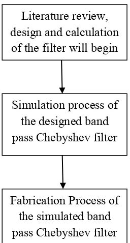
1.5Methodology
The designing process is divided into three stages:
In the first stage, a literature review will be done regarding the Chebyshev filter designing and the architecture of microstrip bandpass is selected. The dimensions, characteristic impedance and relative permeability of the material for bandpass filter will be calculated according to the design specifications.
In the second stage, the bandpass filter will be modeled by using Ansoft Designer according to the design specifications. The bandpass is then simulated for the system characteristic such as insertion loss, center frequency etc.
[image:23.595.258.386.478.717.2]In the third stage, the fabrication of the simulated filter will commence. Tests will be done where by the individual parameters of band pass filter will be measured for verification with the parameter value that are specified in the filter.
Figure 1.1 below shows the flow of the designing process discussed above.
Figure 1.1: Designing Processes Literature review, design and calculation
of the filter will begin
Simulation process of the designed band pass Chebyshev filter
5