DOI: 10.12928/TELKOMNIKA.v14i1.3676 449
Design of AC Charging Interface and Status Acquisition
Circuit for Electric Vehicles
Kun Xu*1, Li Li2
1
Zhoukou Normal University, 466001, Zhoukou, Henan, P. R. China
2
Zhoukou Senior Technical School, 466000, Zhoukou, Henan, P. R. China *Corresponding author, e-mail: [email protected], [email protected]
Abstract
To address the unreliable charging of new charging interfaces caused by comprehending deviation on China’s alternating current (AC) charging interface standard for electric vehicles, implementation methods of AC charging interface circuit, control pilot (CP) circuit, and status acquisition circuit for electric vehicles were proposed in this study. Basic principle and functions of the CP circuit were discussed, and influences of resistance parameters on voltage state at test point were analyzed. Freescale MC9S12XEQ512 was used as the main controller, and its integrated pulse-width modulation module and analog-to-digital converter module were used to simplify circuit designs. An experimental test on charging interface connection confirmation, CP, output power parameter passing, and real-time charging connection status acquisition was conducted on real vehicles. Results demonstrated that the designed circuits exhibit high security and meet the basic requirements of GB/T20234-2 with regard to AC charging interface characteristics. All test data are within the allowed error range. Furthermore, real-time monitoring of the charging process and security isolation design of signals can effectively improve the system stability. Hence, this technology can be used in AC charge control of electric vehicles.
Keywords: electric vehicles, AC charging spot, connection confirmation, control pilot
Copyright © 2016 Universitas Ahmad Dahlan. All rights reserved.
1. Introduction
Given the serious situations of energy crisis and atmospheric pollution problems, positive development of electric vehicle industry and promotion of transportation energy structure upgrading conform to the development of sustainable global energy [1-3]. Compared with traditional vehicles, electric vehicles present incomparable advantages in energy conservation and emission reduction, as well as in reducing dependence on fossil energy [4-7]. With the rapid growth of electric vehicles, the electric vehicle industry is becoming the largest business model of energy network. Hence, charging technology and construction of related facilities of electric vehicles have attracted considerable attention from national governments, automobile manufacturers, research institutes, and power enterprises [8-10]. Considering the vigorous promotion of the Chinese government, electric vehicles have developed from the introduction stage into the comprehensive acceleration stage. Electric vehicle holdings in China are predicted to exceed 5 million by 2020 [11]. The electric vehicle holdings will reach 60 million by 2030, and the total power consumption is 135 billion kWh, which accounts for nearly 1.3% of the estimated national power consumption in 2030 [10].
2. State of the Art
(AC) charging of electric vehicles. On the basis of the embedded microcontroller and real-time operating system μC/OS II, References [16-17] used an actual application as background and designed an AC charging spot for electric vehicles based on embedded technology. Substantial research provides good guiding significance for the construction of electric vehicle charging equipment and corresponding infrastructures. However, different executive standards during R&D restrict the development of electric vehicle industry to a large extent. In accordance with the basic requirements of GB/T20234-2 and the characteristics of AC charging spot interface, CC, and CP, an AC charging control system for electric vehicles was designed, which takes the Freescale-based low-power microcontroller MC9S12XEQ512 as the core. This design mainly includes charging cable CC circuit of the charging spot and CP circuit for communication between charge spot and vehicle-mounted charger. This design was tested on the pure electric-driven passenger vehicles produced by Chery Automobile Co., Ltd. (SQR7000BEVJ00), which realized real-time monitoring of electric vehicle charging, signal security isolation, high-efficiency energy conservation, and intelligent operation. This design presents certain reference values for R&D of electric vehicle charging equipment, as well as corresponding infrastructure construction.
The rest of this paper is organized as follows. Chapter III discusses the AC charging connection status of electric vehicles and explains the equivalence principle of AC charging CP interface of charging pattern 3 and connection mode B. Chapter IV demonstrates the AC charging interface circuit for electric vehicles and designs charging CC, CP, and status acquisition circuit. Chapter V introduces the flowchart of the system test program. Chapter VI illustrates the designed circuits and presents the test results and errors. Chapter VII elaborates the conclusions drawn from this study. Finally, Chapter VIII presents the acknowledgment.
3. AC Charging Status Analysis of Electric Vehicles
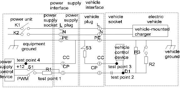
The CC circuit of AC charging cable of electric vehicle and the CP circuit between charging spot and vehicle-mounted charger are preconditioned of information exchange between the charging spot and the charge, as well as the battery management system. The equivalent principle of the typical CP interface of charging pattern 3 and connection mode B is shown in Figure 1 [18].
Figure 1. Equivalent principle diagram of charging spot interface cable connection
The CC of charging plug of the connection mode B can be divided into plug CC of the supply terminals and plug CC of the vehicle. These plugs can be determined by voltage status at test point 4 (Figure 1). The voltage at test point 1 on the CP is the basis for power supply unit (charging spot) to determine the vehicle charging connection status. The voltage at test point 1 is mainly determined by charging cable connection status, as well as status of switches S2 with
R1, R2, and R3. Three states were discussed according to charging process.
State 2: Charging cable plug is connected completely, and S2 is disconnected (the vehicle is not prepared well for charging). The vehicle cannot be charged. As shown in Figure 2, U1 is determined by Equation (1).
(1)
Where R1 and R3 are nominal values in the national standards of 1000 and 2740 ,
respectively. U is the nominal voltage +12 V, which is calculated as V.
State 3: Charge cable plug is connected completely, and the vehicle is prepared well for charging. S2 is closed, and the vehicle can be charged. At this moment, U1 can be calculated from Equation (2) and (3).
(2)
(3)
Where the nominal value of R2 is 1300 . Therefore, V when U=+12V. In
Equations (2) and (3), the internal resistance of D1 on CP and effect of tube voltage drop on U1
are neglected.
Test point 2 and test point 3 are located on vehicles. Whether the vehicle plug and socket are connected successfully is assessed by measuring the resistance of RC at test point 3. According to national standard, RC is 680 Ω/0.5 W or 220 Ω/0.5 W. The corresponding charging cable capacities are 16 A and 32 a.
4. Hardware Circuit Analysis Design 4.1. CC Circuit of Power Supply Interface
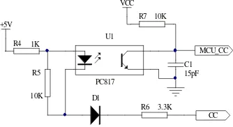
The power supply plug CC circuit is shown in Figure 2. When the power supply plug and socket are connected successfully, the CC and equipment form a short circuit. Meanwhile, +5 V, R4, R5, D1, R6, and the equipment form a loop. The photoelectric coupler PC817 is operated at low MCU_CC level. Briefly, the test point 4 in Figure 2 is at low level. Otherwise, the MCU_CC level is high. Therefore, the processor can determine whether the power supply plug and socket are connected successfully only by testing the MCU_CC level.
Figure 2. Power supply plug CC circuit diagram
4.2. CP Interface Circuit
The CP circuit should be able to output stable +12 V and am bipolar pulse-width modulation (PWM) signal. Under the PWM state, CP circuit requires the peak and valley voltages of +12 V and −12 V. The interface circuit is shown in Figure 3. With the MC9S12XEQ512 integrated PWM pin, the signal is isolated by the high-speed photoelectric coupler 6N135 and is amplified by the push/pull power amplifier composed of Q1 and Q2, and finally output from the CP end. R1 selects the nominal value of 1000 . The CP circuit outputs +12 and −12 V alternatively under the control of logic level state of PWM wave. When the duty ratio of PWM is 50%, the tube voltage drop of Q1 and Q2 is neglected. The relationship between output voltage and level of PWM wave is shown in Figure 4.
Figure 3. CP circuit Figure 4. Relationship between the output voltage of CP port and the level of PWM wave
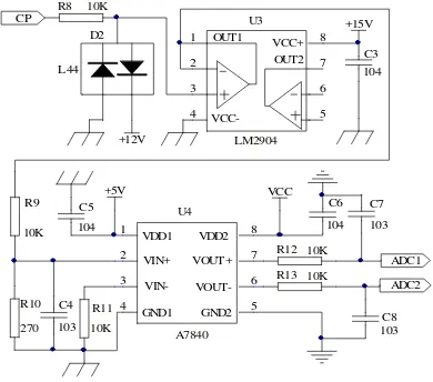
4.3. CP Parameter Acquisition Circuit
This circuit is mainly used for collecting CP state, voltage of PWM wave, and duty ratio. Status and supply power of charging spot and charging equipment are also obtained. The circuit mainly includes a voltage clamp circuit composed of L44, voltage follower composed of integrated operational amplifier LM2904, and linear isolating amplifying circuit composed of linear amplifying photoelectric coupler A7840. The circuit principle is shown in Figure 5.
Figure 5. CP parameter acquisition circuit
As shown in Figure 5, A7840 integrated with input amplifying circuit and photocoupling circuit exhibits high input impedance, good linearity, and approximately 1000 voltage amplification factor. This coupler can realize distortion-less transmission of mV voltage and current signal, thereby using the differential signal output mode. In addition, R9 and R10 form the linear voltage attenuation circuit that can attenuate the collected signal voltage below 320 mV. Consequently, input impedance matching of A7840 is achieved, and the requirements of VIN+ port on input voltage are met. The differential output voltage signals are transmitted into pins of analog-to-digital converter (ADC) (ADC1 and ADC2) of the main controller MC9S12XEQ512. The ADC module integrated in MC9S12XEQ512 conducts real-time acquisition and analysis of the input signal to determine different statuses during AC charging process of electric vehicles.
5. System Program Flow
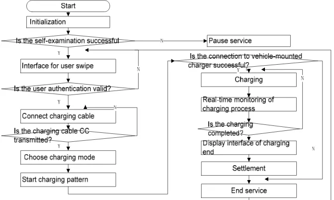
The system program mainly includes system initialization, system self-inspection, user information identification, system CC, and real-time monitoring of charging process (Figure 6). In user information identification, radio frequency identification technology was used for user
information reading, confirmation, and settlement. The real-time monitoring of charging process is mainly applied for real-time acquisition and processing of CP signal, as well as for determining the connection status of charging cable and status of the powered device. Moreover, other circuit modules of the device are monitored to process emergency situations timely and to ensure safety of charging equipment and powered devices.
Figure 6. System program flow
6. Test Result Analysis
All functional modules in the system were tested under loaded conditions. Millivoltmeter and storage oscilloscope were used for parameter observation and recording of testing modules. The pure electric-driven passenger vehicle (SQR7000BEVJ00) made by Chery Automobile Co., Ltd. was used as the charging loading. The DPO7254C oscilloscope (Tektronix) was used for waveform observation. The simulation bandwidth and sampling rate of this oscilloscope are 2.5 GHz and 40 GS/s, respectively. Additionally, communication data were tested, and functions were analyzed using the computer serial debugging tool.
6.1. State Test and AD Application Analysis
The test results are listed in Table 1. The effective values of U1 in Figure 2 under different states represent a nominal value of ±0.8 V. The actual test values under three states are within the effective range and are lower than the nominal voltage, primarily because the +12 V voltages will generate a certain tube voltage drop on Q1.
ADC1 and ADC2 are differential signal (including differential + and differential −) output ends of CP parameter acquisition circuit and are input ends of DC. Therefore, ∆U = (differential +) − (differential −). The equipment state can be evaluated as long as large voltage differences among three ∆U values are enough. In this system, the ADC module uses 8 bits. In the corresponding sampling voltage range (0–5 V), voltage resolution is 5/255≈0.0196 V. AD sampling test results are shown in Table 2. When the analog voltage difference is higher than 0.02 V, different conversion results will be obtained. As shown in Table 1, ∆U differences of three states are all higher than 0.8 V. As a result, the probability of state misjudgment can be reduced significantly according to collected signal by designed circuits.
Table 1. CP state voltage test results
CP
state Signal nominal value/V
Signal range (UMin, UMax)/V
Measured U1
/V ADC1/V ADC2/V ∆U /V
State 1 12 (11.2, 12.8) 11.56 3.76 1.33 2.43
State 2 9 (8.2, 9.8) 8.60 3.39 1.79 1.60
Table 2. AD sampling test results
Analog voltage
U /V - 1.58 1.59 1.60 1.61 1.62 1.63 - 2.43
AD results
Hexadecimal - 0x53 0x53 0x54 0x54 0x55 0x55 - 0x7B
State State 2 State 1
6.2. CC and PWM State Waveform Test
Images of charging cable connection and CP waveform are shown in Figure 7-10. Waveform is found at test point 4 when the power supply plug is connected accurately, as shown in Figure 7. The power supply plug is assumed to be connected completely as long as MCU_CC determines that the voltage is converted from high level to low level.
At this moment, the vehicle plug is not connected, and the CP circuit is under PWM state. The observed waveform is shown in Figure 8. The initial duty ratio is 15%, and the corresponding waveform voltage peak-to-peak (PK-PK) is 22.9 V. The positive peak voltage is 11.45 V, which corresponds to State 1 in Table 1 and is in accordance with the measured data in Table 1.
Figure 7. CC signal test waveform Figure 8. PWM waveform of State 1
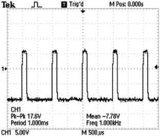
The PWM waveform at test point 1 from State 1 to State 2 is shown in Figure 9. The PK-PK is 17.6 V, and the positive peak voltage is 8.8 V, which matches State 2 in Table 1. The vehicle is well prepared for charging, and S2 is closed. The PWM waveform at test point 1 from State 2 to State 3 is shown in Figure 10. The positive peak voltage is 5.8 V, which corresponds to State 3 in Table 1. Vehicle charging is initiated.
During the charging process, the main controller conducts real-time detection of CC signal and CP signal states in the following order: discover abnormal phenomena, separate AC trigger timely, and stop charging. The test results indicated that the designed circuit meets the basic requirements of GB/T20234-2 and the AC charging spot interface characteristics of the CP. Test data of circuit output are all within the allowed error range.
7. Conclusion
In this study, an AC charging interface circuit and control system is designed using Free scale MC9S12XEQ512 as microcontroller for an electric vehicle. The operating principle and basic functions of the CP circuit are analyzed. This design realizes power supply plug CC and CP during AC charging of electric vehicles and accomplishes real-time acquisition of charging state parameters. In this circuit design, the digital and analog parts are isolated by a photoelectric coupler. As a result, mutual interference decreased, whereas system stability increased effectively. Overall, this design guarantees safe and reliable operation of equipment during charging process.
Acknowledgements
This work was supported by School based project of Zhoukou Normal University in 2015 (Project Number: ZKNUB215101).
References
[1] Yang Haiying, Zhao Anguo, Zhou Hualiang, Xia Yu, Ding Zhigang. Design of AC portable wall-box for electric vehicle. Power Supply Technology and Its Application, 2014; 40(2): 65-67.
[2] Li S, Mi CC. Wireless power transfer for electric vehicle applications. IEEE Journal of Emerging and Selected Topics in Power Electronics, 2015; 3(1): 4-17.
[3] Bessa RJ, Matos MA. Economic and technical management of an aggregation agent for electric vehicles: a literature survey. European Transactions on Electrical Power, 2012; 22(3): 334-350. [4] HE Zhi-gang, ZHAO Ming-xing, XU Xing, XU Jian-feng. Study on EV interior noise based on transfer
path analysis. Science Technology and Engineering, 2014; 14(21): 156-161.
[5] HU Zechun, SONG Yonghua, XU Zhiwei, LUO Zhuowei, ZHAN Kaiqiao, JIA Long. Impacts and utilization of electric vehicles integration into power systems. Proceedings of the CSEE. 2012; 32(4): 1-10.
[6] Pham Cong Thanh, AnWen Shen, Phan Quoc Dzung, NB Anh. Self-Tuning Fuzzy PI-Type Controller in Z-Source Inverter for Hybrid Electric Vehicles. International Journal of Power Electronics and Drive Systems. 2012; 2(4): 353-363.
[7] FR Islam, HR Pota. Impact of Dynamic PHEV load on Photovoltaic System. International Journal of Electrical and Computer Engineering. 2012; 2(5): 644-654.
[8] Khodayar ME, Wu L, Shahidehpour M. Hourly coordination of electric vehicle operation and volatile wind power generation in SCUC. IEEE Transactions on Smart Grid. 2012; 3(3): 1271-1279.
[9] Rotering N, Ilic M. Optimal charge control of plug-in hybrid electric vehicles in deregulated electricity markers. IEEE Transactions on Power Systems. 2011; 26(3): 1021-1029.
[10] ZHANG Yan-yu, ZENG Peng, ZANG Chuan-zhi. Coordinated optimal charging algorithm for electric vehicles in smart grid. Science Technology and Engineering. 2015; 15(26): 60-65.
[11] Tan Xiaobo, Zhao Hai, Peng Haixia, Li Dazhou. Quasi-real-time coordinated charging/discharging policy for electric vehicles. Transactions of China Eleetrotechnical Society. 2015; 30(13): 69-76. [12] Robert (Bob) Bruninga. Overlooking L1 Charging At-Work in the Rush for Public Charging Speed.
Electric Vehicle Conference (IEVC). 2012: 1-5.
[13] SANG Lin, XU Hong-hai, GUAN Xiang. Experiment design on control pilot circuit of AC charging coupler for electric vehicle. Electrical Measurement & Instrumentation. 2013; 50(2): 112-115.
[14] YUAN Jinyun, WANG Xiangdong, WANG Dongqing, WANG Haiming. Research on AC charge spot control system for electric vehicle based on PLC. Journal of Qingdao University (E&T). 2015; 30(2): 38-41.
[15] DU Jiang, WANG Gang, WANG Jinqin. Application of ARM embedded industrial control module in AC charge spot for electric vehicle. Low Voltage Electrical Apparatus. 2013; 16: 48-52.
[16] FAN Xiao-yan, DING Li-bo, MA He-xiang, ZHANG Wen-hui. Design of AC charging spot for electric vehicles based on embedded system. Modern Electronics Technique. 2012; 36(16): 178-180.