XRD Analysis of Cu-Al Interconnect Intermetallic Compound in an
Annealed Micro-Chip
KOK YAU CHUA
1, a, MAY TING HNG
2, b, CHER CHIA LEE
2, cand T. JOSEPH SAHAYA ANAND
1,d1
Faculty of Manufacturing Engineering, Universiti Teknikal Malaysia Melaka, Hang Tuah Jaya, 76100 Durian Tunggal, Melaka, Malaysia
2
Infineon Technology (Malaysia) Sdn. Bhd., FTZ Batu Berendam, 75350 Melaka, Malaysia
a transmission electron microscope (TEM) and energy dispersive X-ray (EDX). In XRD analysis, peak correspond to CuAl phase is identified from measurement with slower scan configuration. The difficulty for IMC peak detection in diffractogram is due to low composition ratio of IMC relative to other materials available in the sample. KOH treatment for enhancing IMC peaks intensity does not work as expected as it etches the IMC as well.
Introduction
Thermosonic Copper (Cu) wire interconnection technology has been extensively developed since 80’s in semiconductor industry [1,2]. The purpose is to replace expensive gold (Au) wire while maintaining the reliability and performance of the products. From material point of view, Cu possesses some better physical properties relative to gold. Table 1 shows the comparison of material properties between these materials [3]. Better heat and electrical conductivities allow application of copper wire for high power and faster chip functionality [4].
Table 1: Material properties comparison between Cu and Au [3]
Material properties Cu Au
Thermal conductivity (Wm-1K-1) 398 315
Electrical conductivity (107 Ω-1m-1) 6.0 4.3
Modulus of elasticity (GPa) 110 77
Specific heat, cp (Jkg-1K-1) 386 128
Linear coefficient of Thermal Expansion (10-6K-1) 17.0 14.2
Thermosonic (Thermal + Ultrasonic) wire bonding technique has been a well-known interconnection method in the industry. It is to join the wire material onto bond pad metallization on a microchip [5,6]. The bonding mechanism is explained in [7]:
1. Formation of Free Air Ball (FAB) by Electric Frame Off (EFO) process that uses electrical sparks to melt the wire tip into a symmetrical sphere.
2. Mechanical compression of the FAB by a capillary against the bond pad metallization with a pre-set force and ultrasonic power. Ultrasonic vibration causes softening of the FAB and thus its plastic deformation.
3. Scrubbing between FAB and bond pad metallization removes contamination and oxides on metallization surface and form new intermetallic phase at the interface. This new phase anchors the FAB and bond pad metallization which promoting bonding at the interface.
In semiconductor industry, aluminum metallization is commonly used as bond pad for wire interconnection. It serves as the Input/output terminal (I/O) that connects external circuit through the bonded wires. Bonding reliability of Cu wire-Al bond pad (Cu-Al) configuration is a common interest for researchers and extensive studies has been carried out [8,9]. Cu wire bonding on Al bond pad can be challenging in manufacturing. Cu wire is easily oxidized during EFO process which involves high temperature generation. Counter measure for this difficulty is to perform EFO in inert environment. In this context, “copper kit” is invented to serve this purpose. Copper kit is a facility that enables flow of inert gas around the region of EFO so that oxygen is isolated from this region and Cu FAB oxidation is avoided. Common inert gas used in industry is Forming Gas, i.e. mixture of 95% N2 and 5% H2 [8]. According to Inderjit et al [10], oxidation of Cu FAB results in Non-Stick On Pad (NSOP) issue that cause yield loss in manufacturing. Necessity of Forming Gas flow in Cu wire bonding is considered as additional critical process parameter and also investment. Besides, it is reported that mechanical pressure and ultrasonic vibration on harder Cu FAB against Al bond pad could generate excessive Al bond pad deformation or “Al splash” and damage of structure under bond pad [7,11,12]. Al splash potentially result in short circuit as deformed Al may in contact with adjacent wires [12]. This is particularly important for fine pitch a device which has small distance between adjacent wires. Moreover, Al bond pad thickness reduction caused by Al splash at higher stress region results in tendency of damage of the structure under bond pad [7]. Occurrence of these failures could be minimized by reducing the process parameters, however, this compromise the mechanical shear strength of the Cu/Al bonding. This reflects the limited process window of Cu wire bonding in semiconductor manufacturing [12].
For system that Cu wire interconnects on Al bond pad metallization, the condition of IMCs which comprise of both elements is relatively complicated than pure Cu wire and Al metallization. These IMCs generally show more complex crystallographic structures e.g. CuAl2 phase with tetragonal unit cell geometry but three possible symmetries (with space groups of P4/mmm, I4/mcm and Fmmm) compare to that of pure Cu and Al in face center cubic (fcc) [2]. Moreover, it is reported that the IMCs possess significantly different electrical resistivity [7], hardness and thermal conductivity [13] compare to that of pure materials [3,7]. The as bonded intermetallic will grow or thicken by interdiffusion over the time if the system is subjected to thermal treatment or when the micro-chip is in service. Excessive growth of IMC leads to increase of contact resistance and thus affecting the electrical performance of the chip [4,7,9]. It is important to assess the IMC development over time to ensure the functionality and reliability of the device. In this context, a standard test is employed in semiconductor industry, i.e. High Temperature Storage (HTS) test. HTS is an isothermal aging process with typical temperature of 175°C that is suitable to assess the IMC growth for long term reliability monitoring of electronic devices.
In this paper, the possibility of common XRD technique to analyse the IMC that exist at the Cu-Al bonding interface is studied. Due to thin IMC formed at the bonding interface as discussed above, it is reasonably expected low intensity of the relevant peaks. Therefore, several methods including XRD configuration and sample material preparations are assessed for enhancing the IMC peaks visibility in the diffractogram.
Materials and Methodology
Diode microchips (Si chip) with pure Al bond pad were first transferred from wafer to leadframe by normal die bonding process. Then the samples were bonded with 22µm 5N (purity of 99.999%) Copper wire. The wire bonding process was carried out on a commercially available Shinkawa ACB-35 wire bonder with Cu kit from the machine maker. Bonding parameters used in this sample preparation has been established for manufacturing. Prepared samples were inspected to ensure no bonding issue e.g. Non-Stick On Pad (NSOP) and copper FAB oxidation. Wire bonded samples were then loaded into HTS chamber at 175°C for 500 hours to promote growth of IMC. For some portion of the annealed samples, the Si chips and Cu wires were peeled manually using tweezer. This type of samples was then crashed into powder form with mortar and pestle. This is to enables random orientation of the grains of the materials in the sample. On the other hand, another portion of annealed sample which without removal of Si chip and Cu wire was used directly for XRD analysis. This type of sample was then called non-powder sample.
Furthermore, visibility of Cu-Al IMC peaks could be enhanced if other materials in the sample which are not interested can be removed before XRD measurement. In this context, hot KOH etching was evaluated to remove unwanted material from the powder sample, i.e. Si, SiO2 and Al pre-deposited on the Si chip. 2.5wt% KOH solution was heated to 80°C and etching of ~2g of powder sample was performed at this temperature. The etching ended when there was no generation of H2 bubbles.
XRD equipment used in this study was XPERT-PRO by PANalytical with monochromatic Cu kα radiation. The equipment is configured in θ/2θ (Bragg–Brentano goniometer) geometry. Evaluations were performed for various sample types, i.e. powder, non-powder and etched powder form. Moreover, effect of different scanning rate of the measurement is evaluated on selected sample. Diffractograms generated in XRD measurement were analysed using X’Pert High Score Plus software.
To understand the actual IMC condition in the sample, one unit of sample was sent for TEM inspection. This unit was mechanical cross-sectioned until Cu wire, Al bond pad and Si chip were visible. Then the cross-sectioned sample was sent for focus ion beam (FIB) for lamella preparation. The lamella with dimension of (10µm x 10µm x 0.1µm) was cut from center of ball bond and transfer to TEM sample holder by lift-out method. The lamella was then analysed by transmission electron microscope (TEM) and energy dispersive X-ray (EDX).
Results and Discussion
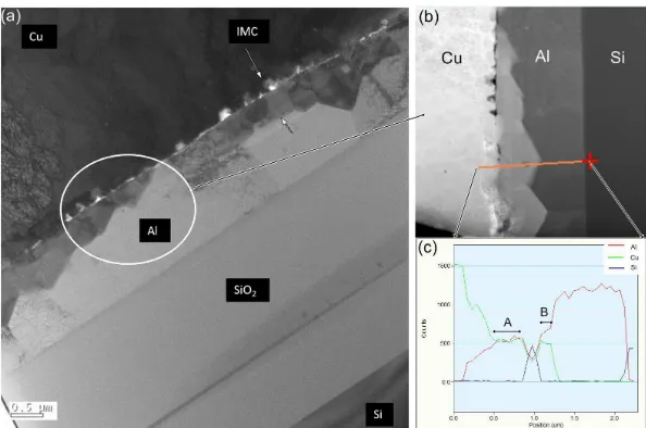
Increase of Si signal intensity at position at 1µm from left side of the scan line is believed due to Si re-deposition during FIB milling. With Fig. 1, it is observed that IMCs are available at the bonding interface of Cu wire and Al bond pad.
Fig. 1: a) TEM image of lamella extracted from center of Cu-Al bonding interface. b) line scan EDX across Cu to Si. c) Signal intensity for Al, Cu and Si elements acorss the line defined in (b).
Fig. 2: Diffractogram of sample in powder form that consists of Cu wires and Si chip.
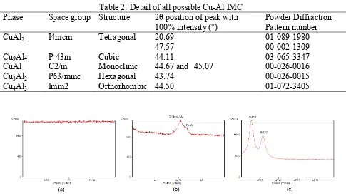
Table 2: Detail of all possible Cu-Al IMC
Phase Space group Structure 2θ position of peak with
100% intensity (°)
Powder Diffraction Pattern number
CuAl2 I4mcm Tetragonal 20.69
47.57
01-089-1980 00-002-1309
Cu9Al4 P-43m Cubic 44.11 03-065-3347
CuAl C2/m Monoclinic 44.67 and 45.07 00-026-0016
Cu3Al2 P63/mmc Hexagonal 43.74 00-026-0015
Cu4Al3 Imm2 Orthorhombic 44.50 01-072-3405
Fig. 3: Diffractograms of selected 2θ ranges with slow scan.
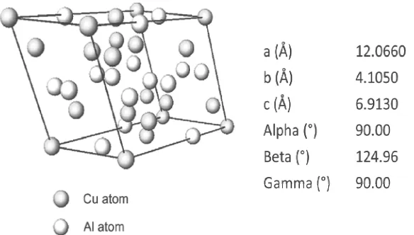
Experiment of XRD measurement of power sample was repeated with slower scan, i.e. step size of 0.002° and scan step time of 127 seconds. To shorten the scanning time, measurement was performed for selective 2θ ranges, i.e. 19-21, 43.5-45.5 and 47-48°. These ranges are corresponding to all possible diffraction angles of Cu-Al IMCs at room temperature with 100% intensities which is more likely to appear theoretically. Table 2 lists all possible Cu-Al IMCs in the samples, their structures and the diffraction angles of peaks of 100% intensity. Results of measurement with slow scanning at these 2θ ranges are shown in Fig. 3 (a) – (c). From these diffractograms, it is observed that a peak corresponding to CuAl phase is detected at 2θ = 44.676° as shown in Fig. 3 (b). Slow XRD scan enhances resolution of diffraction signal over a smaller 2θ range. This allows better visualization of peak that was with weak intensity in the faster scan mode. Besides, slower scan allows increased intensity of diffraction signal which is useful in revealing weak peaks [18]. This peak is corresponding to crystal plane orientation of (-5 1 1) which has 100% intensity in standard pattern in Powder Diffraction File (PDF) database [19]. Full width at half maximum (FWHM) of this peak is 0.0967°. Estimated crystallite size based on FWHM and Scherrer’s equation is 180nm. Fig. 4 illustrates the 3 dimensional model [20] and its lattice parameters [19] of the CuAl phase.
Fig. 4: 3 dimensional crytal model of CuAl and its lattice parameters.
Fig. 5: a) Diffractogram of etched powder sample with faster scan. b) Comparison of diffractogram of unetched and etched powder samples.
Conclusion
Investigation of thin Cu-Al IMC existed at the bonding interface of Cu wire-Al bond pad usually incurs expensive investment for sample preparation and analysis. The attempt of analysing the IMC using common XRD technique in θ/2θ geometry configuration is demonstrated. TEM analysis was first performed on sample that underwent HTS annealing at 175C for 500 hours. It is confirmed that mixture of CuAl and CuAl2 phases are available at the bonding interface by TEM analysis. Diffractogram from powder sample shows a peak that corresponds to CuAl phase only when it is configured to slow scan for specific 2θ range. This is due to low composition ratio of Cu-Al IMC relative to other materials. 2.5wt% KOH etching for removal of uninterested materials did not work as expected as it removes the IMC as well.
Acknowledgement
References
[1] J. Onuki, M. Koizumi, I. Araki: IEEE Trans. Compon., Hybrids and Manuf. Technol. Vol 10 (1987) p. 550
[2] H. Xu, C. Liu, V.V. Silberschmidt, S.S. Pramana, T.J. White, Z. Chen, V.L. Acoff: Acta. Mater. Vol 59 (2011) p. 5661
[3] W.D. Calister Jr., Materials Science and Engineering An Introduction, sixth ed., John Wiley & Sons Inc., New York, 2004.
[4] H. Xu, C. Liu, V.V. Silberschmidt, Z. Chen: J. Electron. Mater. Vol 39 (2010) p. 124
[5] L.T. Nguyen, D. McDonald, A.R. Danker, P. Ng: IEEE Trans. Comp. Pack. Manuf. Technol., Vol 18 (1995) p. 423
[6] S. Murali, N. Srikanth, C.J. Vath III: Mater. Charact. Vol 50 (2003) p. 39
[7] C.D. Breach, F.W. Wulff: Microelectron. Reliab. Vol 50 (2010) p. 1
[8] F.W. Wulff, C.D. Breach, D. Stephen, Saraswati, K.J. Dittmer: 6th Proc. of Electron. Packag. Technol. Conf., 8-10 Dec. 2004, p. 348
[9] C.J. Hang, C.Q. Wang, M. Mayer, Y.H. Tian, Y. Zhou, H.H. Wang: Microelectron. Reliab. Vol 48 (2008) p. 416
[10] S. Inderjit, J.Y. On, L. Levine: 55th Proc. of Electron. Comp. and Technol. Conf., 31st May – 3rd June 2005, p. 843
[11] G.E. Servais, S.D. Brandenburg: 17th Int. Symp. for Test. and Fail. Anal., Los Angeles, 11-15 November 1991, p. 525
[12] H. Clauberg, P. Backus, B. Chylak: Microelectron. Reliab., Vol 51 (2011) p. 75
[13] M.H.M. Koutersa, G.H.M. Gubbels, O. O'Halloran, R. Rongen: 18th Eur. Microelectron. and Packag. Conf., 12-15th September 2011
[14] M. Drozdov, G. Gur, Z. Atzmon, W.D. Kaplan: J. Mater. Sci., Vol 43 (2008) p. 6029
[15] J.L. Murray: Int. Mat. Rev., Vol 30 (1985) p. 211
[16] D.C. Gray, J.W. Butterbaugh, F.C. Hiatt, A.S. Lawing, and H.J. Sawin: Electrochem. Soc. Vol 142 (1995) p. 3919
[17] J. Buhlery, F.P. Steiner and H. Baltes, J. Micromech: Microeng. Vol 7 (1997) p. 1
[18] Sharma, P.K., Hickey, G.S., http://hdl.handle.net/2014/31696
[19] JCPDF # 00-026-0016
[20] J. Chen, Y.S. Lai, Y.W. Wang, C.R. Kao: Microelectron. Reliab. Vol 51 (2011) p. 125