Three Bit Subtraction Circuit
via Field Programmable Gate Array
A. Jaafar
1, N. Arasid
2, N. M. Z. Hashim
3, A. A. Latiff
4, Hazli Rafis
51, 2, 3, 4, 5
Faculty of Electronics & Computer Engineering, Universiti Teknikal Malaysia Melaka,
Hang Tuah Jaya, 76100 Durian Tunggal, Melaka, Malaysia.
1
[email protected], [email protected]; 3
[email protected], [email protected],
Abstract: This project is about to design the software and hardware simulator for a Three Bit subtraction Circuit via Field Programmable Gate Array (FPGA). The three bit subtraction circuits are involved in performing the subtraction for each bit by performs operation the arithmetic and logic unit, called the Arithmetic Logic Unit (ALU). All this operation is to be displayed at seven segment using FPGA board by using Verilog language. A FPGA is a semiconductor device containing programmable logic components called "logic blocks", and programmable interconnects. Logic blocks can be programmed to perform the function of basic logic gates such as AND, and XOR, or more complex combinational functions such as decoders or simple mathematical functions such as additional, subtraction, multiplication, and divisions (+, -, x, ÷). In conclusion, three bit subtraction circuit via FPGA has been successfully designed and developed. In order to have a complete system that is design by our own, one of the recommendation to enhance the possibility of this thesis is to develop the hardware equip with wireless technology.
Keywords: Arithmetic Logic Unit (ALU), Field Programmable Gate Array (FPGA), Logic Block, Subtraction Circuit, Verilog.
1.
INTRODUCTION
This project is to design the software and a hardware simulator for a three bit subtraction Circuit via FPGA. The designing the three bit subtraction circuit are involved in performing the subtraction for each bit by performs operation the arithmetic and logic unit, called the Arithmetic Logic Unit (ALU) example Addition, Subtraction, Multiplication and Division. All this operation is to display at seven segment using FPGA board by using Verilog language [1], [2]. A FPGA is a semiconductor device containing programmable logic components called "logic blocks", and programmable interconnects. Logic blocks can be programmed to perform the function of basic logic gates such as AND, and XOR, or more complex combinational functions such as decoders or simple mathematical functions (+, -, x, ÷). In most FPGAs, the logic blocks also include memory elements, which may be simple flip-flops or more complete blocks of memories. Combination of FPGA and ALU will produce the design of three bit
subtraction circuit via FPGA [3]. The purpose of designing three bit subtraction is in order to do operation of subtraction three bits are needed e.g. 2 – 0 = 2 the integer is representing as bits. These three bits will be implemented as logic gates in order to obtain the result of subtraction[4]. The problem that been discussed in this issue was FPGAs are usually slower than their application-specific integrated circuit (ASIC) counterparts, as the capability to handle a complex task [5]. Two bits for subtraction will not represent any result. Therefore to obtain the result the minimum number of bits to be used is three bits.
2.
LITERATURE REVIEW
functions such as decoders or simple mathematical functions [7]. In most FPGAs, the logic blocks also include memory elements, which may be simple flip-flops or more complete blocks of memories. A hierarchy of programmable interconnects allows logic blocks to be interconnected as needed by the system designer, somewhat like a one-chip programmable breadboard [8], [9], [10]. Logic blocks and interconnects can be programmed by the customer or designer, after the FPGA is manufactured, to implement any logical function hence the name "field-programmable"[6]. FPGAs are usually slower than their application-specific integrated circuit (ASIC) counterparts, as they cannot handle as complex a design, and draw more power. But their advantages include a shorter time to market, ability to re-program in the field to fix bugs, and lower non-recurring engineering costs [11]. Vendors can sell cheaper, less flexible versions of their FPGAs which cannot be modified after the design is committed [12], [13], [14]. The designs are developed on regular FPGAs and then migrated into a fixed version that more resembles an ASIC. Another alternative are complex programmable logic devices (CPLDs) and Xilinx Sparta-II FPGA is used as the tools.
2.1.Applications of FPGA
Applications of FPGAs include digital signal processor DSP, software-defined radio, aerospace and defense systems, ASIC prototyping, medical imaging, computer vision, speech recognition, cryptography, bioinformatics, computer hardware emulation and a growing range of other areas. FPGAs originally began as competitors to CPLDs and competed in a similar space, that of glue logic for PCBs. As their size, capabilities, and speed increased, they began to take over larger and larger functions to the state where some are now marketed as full systems on chips (SOC) [15]. FPGAs especially find applications in any area or algorithm that can make use of the massive parallelism offered by their architecture. One such area is code breaking, in particular brute-force attack, of cryptographic algorithms. FPGAs are increasingly used in conventional High Performance Computing applications where computational kernels such as FFT or Convolution are performed on the FPGA instead of a microprocessor. The use of FPGAs for computing tasks is known as reconfigurable computing [6]. The inherent parallelism of the logic resources on the FPGA allows for considerable compute throughput even at a sub-500MHz clock rate
[16], [17]. For example, the current (2007) generation of FPGAs can implement around 100 single precision floating point units, all of which can compute a result every single clock cycle. The flexibility of the FPGA allows for even higher performance by trading off precision and range in the number format for an increased number of parallel arithmetic units. This has driven a new type of processing called reconfigurable computing, where time intensive tasks are offloaded from software to FPGAs. The adoption of FPGAs in high performance computing is currently limited by the complexity of FPGA design compared to conventional software and the extremely long turn-around times of current design tools, where 4-8 hours wait is necessary after even minor changes to the source code [7].
2.2.FPGA Architecture
Modern FPGA families expand upon the above capabilities to include higher level functionality fixed into the silicon. Having these common functions embedded into the silicon reduces the area required and gives those functions increased speed compared to building them from primitives. FPGAs are also widely used for systems validation including pre-silicon validation, post-pre-silicon validation, and firmware development. This allows chip companies to validate their design before the chip is produced in the factory, reducing the time to market.
2.3. FPGA design and programming
To define the behavior of the FPGA the user provides a hardware description language (HDL) or a schematic design. Common Verilog [18], [19]. The user will validate the map, place and route results via timing analysis, simulation, and other verification methodologies. Once the design and validation process is complete, the binary file generated (also using the FPGA company's proprietary software) is used to (re)configure the FPGA. To simplify the design of complex systems in FPGAs, there exist libraries of predefined complex functions and circuits that have been tested and optimized to speed up the design process. These predefined circuits are commonly called IP cores, and are available from FPGA vendors and third-party IP suppliers. Figure 1 illustrates the Internal Architecture of FPGA. The purpose of programmable logic block in a FPGA is to provide the basic computation and storage elements used in digital systems. The basic logic element contains some form of programmable combinational logic, a flip-flop or latch and some fast carry logic to reduce area and delay cost to it could be entire processor. In addition to a basic logic block, many modern FPGAs contains a heterogeneous mixture of different blocks, some of which can only be used for specific functions, such as dedicated memory blocks, multipliers or multiplexers; of course, configuration memory is used throughout the logic block to control the specific function of each element within the block.
Figure 1: Internal Architecture of FPGA
2.4. Xilinx Tools
2.4.1. Xilinx Spartan II FPGA
The Spartan II FPGA platform as shown in Figure 2 combines the performance and functionality advantages of SRAM-based technology with reliable on-volatile flash technology in a single-chip solution.
Figure 2: The Spartan-II FPGA platform
Used this board for the implementation of the design and it was fairly easy as the Spartan-II platform provides flexibility.
Figure 3: Xilinx Integrated Software Environment (ISE)
Design Implementation is the process of translating, mapping, placing, routing, and generating a BIT file for the design. The Design Implementation tools are embedded in the ISE software for easy access and project management. Design Implementation tools, and must incorporate placement constraints through a User Constraints File (UCF).
2.5.Subtraction
A good representation for negative numbers makes subtraction hardware much easier to design.
i. Two‟s complement is used most often (although
signed magnitude shows up sometimes, such as in floating-point systems).
ii. Using two‟s complement, it can build a
subtraction with minor changes to the adder from last time.
iii. It can also make a single circuit which can both add and subtracted.
Overflow is still a problem, but signed overflow is very different from the unsigned overflow. Sign extension is needed to properly “lengthen” negative numbers. For example a subtraction circuit that shows below and must understand how to illustrate it and apply to the Verilog coding.
For least-significant bits
(1)
(2)
For least-sign
(3)
(4)
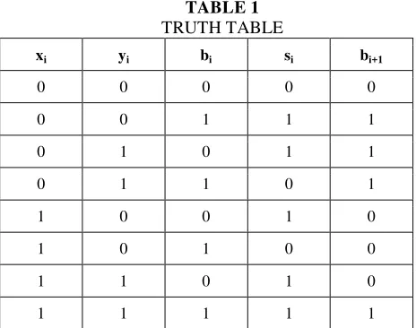
According to Table 1 show an example of truth table where the equation 1 until equation 4 input are used to find the
of
�0, �1,
�1 and��+1.
For example, theequation 2 . Just implement the value given in the truth table and obtain the value.
TABLE 1
TRUTH TABLE
xi yi bi si bi+1
0 0 0 0 0
0 0 1 1 1
0 1 0 1 1
0 1 1 0 1
1 0 0 1 0
1 0 1 0 0
1 1 0 1 0
1 1 1 1 1
Adder is most basic design that is used for subtraction [20]. For example to design a subtraction circuit, the binary value is complimented. Below are the circuit shown and Verilog coding of how it is implemented respectively. Figure 4 shows a design of a subtraction circuit and Figure 5 shows how to convert the subtraction circuit into Verilog coding.
Figure 4: Example design a subtraction circuit
Figure 5: Example Verilog coding
y0 y1 yn–1
y0
c0
cn
y1
yn–1
… … … … x0 x1 xn–1
x0
x1
xn–1
… s1 s0
sn–1
sn–1/dn–1 s1/d1 s0/d0 … adder add/sub ovf/unf 1 1
0
x
y
d
1 1
1
x
y
b
i i
ii
x
y
b
d
i i
ii i
i
x
y
x
y
b
b
1
0 0 1 x y
3.
METHODOLOGY
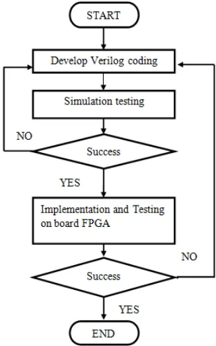
3.1.Methodology flowchart
The project methodology is illustrated in Figure 6. There are few steps that have been involved in order to achieve the objectives of the project. Each project needs suitable strategy on planning in order to run the project smoothly. As soon as the purpose and function of the project are clear, the method of the project is divided into several parts. In this system show the process of developing the coding of three bit subtraction circuit using the Verilog language. This coding is generating using the block diagram that was designed which includes logic gates. Furthermore, after designing the diagram the coding for the design of diagram is developed using the Xilinx ISE software to generate the circuit for three bits subtraction. Once the coding is successful run, the simulation test can be done using generate test bench to test in behavior implementation. If the simulations fail, the result at the waveform can be observed and redesign the test bench or the Verilog coding is needed. Once coding of three bit subtraction is fully finish. The coding will be testing on board FPGA.
Figure 6: Methodology flowchart
From the Figure 7 shows that several step used to design the overall process in designing three bit subtraction. For design entries, it describes each Xilinx constraint, including supported architectures, applicable elements, propagation rules, and syntax examples. It also describes constraint types and constraint entry methods. Provides strategies for using timing constraint and describes supported third party constraints. Design synthesis and behavioral simulation will provide a general overview of designing Field Programmable Gate Arrays (FPGA devices) with Hardware Description Languages (HDLs). It will also include design hints for the novice HDL designer, as well as for the experienced designer who is designing FPGA devices for the first time. Furthermore for design implementation it will describes Xilinx implementation tools and design flows, including the hierarchical flows such as Incremental Design, Modular Design, and Partial Reconfiguration. Includes reference information for Xilinx FPGA and CPLD command line tools, including syntax, input files, output files, and options. Xilinx device programming describes the function and operation of Spartan II devices. Moreover, describes how to achieve maximum density and performance using the special features of the devices which includes information on FPGA configuration techniques and printed circuit board (PCB) design considerations.
Figure 7: Step-by-step through the design process
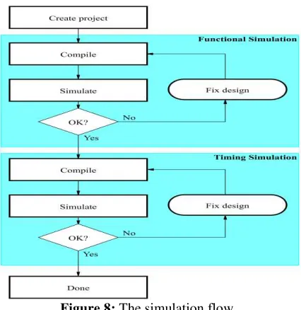
This simulation is fast and useful for checking the fundamental correctness of the designed circuit. The second step of the simulation process is the timing simulation. It is a more complex type of simulation, where logic components and wires take some time to respond to input. In addition to test the logical operation of the circuit.
Figure 8: The simulation flow
3.2.Setting up Xilinx software
Xilinx Tools can be started by clicking on the Project Navigator Icon on the Windows desktop. This should open up the Project Navigator window on the screen. This window shows the last accessed project. From Figure 8 File->New Project is selected to create a new project.
Figure 9: Window Form of Xilinx ISE 10.1
From Figure 9 new project initiations will appear and fill up the necessary entries as follows: Project
Name is used to write the name of new project. Furthermore, Project Location will indicate the entire directory where new project to be stored. HDL Top-level Source Type is chosen.
Figure 10: New Project Initiation window (snapshot from Xilinx ISE software)
From Figure 10 each of the properties given below need to be understood, click on the „value‟ area and select from the list of values that appear. Device Family is Family of the FPGA/CPLD used. In this project the Spartan II FPGA‟s is being used. Device is the number of the actual device. For this project XC2S50 is been enter. Package indicates the type of package with the number of pins. The Spartan FPGA used in this project is packaged in PQ208 package.
The Speed grade is “-6”. Synthesis Tool that was
selected is XST [VHDL/Verilog]. Simulator is the tool used to simulate and verify the functionality of the design. Finally click on NEXT to save the entries.
Figure 11: Device and Design Flow of Project
In the previous window, click on the NEW SOURCE then a window pops up as shown in Figure 12.
Figure 12: Create new source window (snapshot
from Xilinx ISE software)
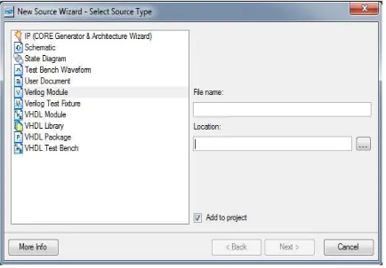
From Figure 13 Select Verilog Module and in the “File Name:” area, enter the name of the Verilog source file to be created. Also make sure that the option Add to project is selected so that the source need not be added to the project again. Then click on Next to accept the entries.
Figure 13: Creating Verilog-HDL source file (snapshot from Xilinx ISE software)
From Figure 14 In the Port Name column, enter the names of all input and output pins and specify the Direction accordingly. A Vector/Bus can be defined by entering appropriate bit numbers in the MSB/LSB columns. Then click on Next> to get a window showing all the new source information. If any changes are to be made, just click on <Back to go back and make changes. If everything
is acceptable, click on Finish > Next > Next > Finish to continue.
Figure 14: Define Verilog Source window (snapshot
from Xilinx ISE software)
From Figure 15 once Finish button is clicked, the source file will be displayed in the sources window in the Project Navigator. If a source has to be removed, just right click on the source file in the Sources in Project window in the Project Navigator and select Remove in that. Then select Project -> Delete Implementation Data from the Project Navigator menu bar to remove any related files.
Figure 15: New Project Information window
(snapshot from Xilinx ISE software)
Figure 16: Language Templates Verilog (from Xilinx ISE software)
3.4. Functional Simulation of Combinational Designs
3.4.1. Adding the test vectors
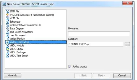
From Figure 17 to check the functionality of a design, testing vectors and simulating the circuit are applied. In order to apply test vectors, a test bench file is written. Essentially it will supply all the inputs to the module designed and will check the outputs of the module. Click „Next‟ to proceed. In the next window select the source file with which want to be associated the test bench.
Figure 17: Adding test vectors to the design (snapshot from Xilinx ISE software)
3.4.2. Simulating and Viewing the Output Waveforms
From Figure 18 now under the Processes window (making sure that the testbench file in the Sources window is selected) expand the ModelSim simulator Tab by clicking on the add sign next to it. Double Click on Simulate Behavioral Model. Compiler error will be in place at the screen. Answer “No” if abort simulation will be chosen. This should cause ModelSim to open. Wait for it to complete execution. If you wish to not receive the compiler error, right click on Simulate Behavioral Model and select
process properties. Mark the checkbox next to
“Ignore Pre-Complied Library Warning Check”.
Figure 18: Simulating the design (snapshot from Xilinx ISE software)
From Figure 19 shows that Verifying Functionality using Behavioral Simulation. Firstly create a test bench waveform containing input stimulus use to verify the functionality of the three bit subtraction module. The test bench waveform is view using graphical view design. In the Sources window, select the Behavioral Simulation view to see that the test bench waveform file is automatically added to the project. Verify that the three bit subtraction design functions as expect by performing behavior simulation. In the Processes tab, click the “+” to expand the Xilinx ISE Simulator process and double-click the Simulate Behavioral Model process. The ISE Simulator opens and runs the simulation to the end of the test bench. Lastly to view the simulation results, select the Simulation tab and zoom in on the transitions.
Figure 19:Simulation Results
3.4.3. Assigning Pins with Constraints
Constraints Editor (PACE) open. Finally select the Package Viewtab.
Figure 20: Construct the pin input output
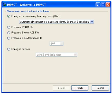
The next is connecting the 5V DC power cable to the power input on the demo board. Then connect the download cable between the PC and demo board. Select Implementation from the drop-down list in the Sources window. After that, select three bit subtraction in the Sources window. In the Process window, double-click the Configure Target Device process. The Xilinx WebTalk Dialog box will open during the process. Click Decline. iMPACT opens and the Configure Devices dialog box is displayed show at Figure 21. In the Welcome dialog box, select Configure devices using Boundary-Scan (JTAG). Verify that automatically connect to a cable and identify Boundary-Scan chain is selected. Then click finish. The devices connected to the JTAG chain on the board will be detected and displayed in the iMPACT window.
Figure 21: iMPACT Welcome Dialog Box
From Figure 22 and Figure 23 shows the last step in the design verification process. This section provides simple instructions for downloading the three bit
subtraction design to the Spartan-II Starter Kit demo board. The progress of the bit stream download will be displayed. The download operation should take less than a minute. When programming is complete, the Program Succeeded message will displayed at Figure 24.
Figure 22: Download of the bit stream to the FPGA
Figure 23: Progress of the bit stream download
Figure 24: Succeeded message
4.
RESULTS AND DISCUSSIONS
4.1.Design three bit subtraction
Implementation of 3 bit subtraction using Verilog HDL and its testing on the Spartan 2 FPGA. Starting the ISE Software. To start ISE, double-click the desktop icon, or start ISE from the Start menu by selecting: Start →All Programs →Xilinx ISE
10.1→Project Navigator Note that design start-up
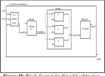
Figure 25 shows that the full block diagram of design which include Binary Adder –Subtraction, Half Adder and Full Adder. The gate level diagram of the 3 bit subtraction was obtained as follows: -
Figure 25: Block diagram for three bit subtraction circuit design
Among the functions encountered are the various arithmetic operations. The most basic arithmetic operation is the addition of two binary digits. This simple addition consists of four possible elementary operations. 0 + 0 = 0, 0 + 1 = 1, 1 + 0 = 1, 1 + 1 = 10. The first three operations produce sum of one digit, but when the both augends and addend bits are equal 1, the binary sum consists of two digits.
A binary adder-subtractor is a combinational circuit that performs the arithmetic operations of addition and subtraction with binary numbers. The circuit will be developed by means of a hierarchical design. The half adder design is carried out first, from which is developed the adder. Connecting n full adders in cascade produces a binary adder for two n-bit numbers. Meanwhile for Half Adder From the verbal explanation of a half adder, this circuit needs two binary inputs and two binary outputs. The input variables designated the augends and addend bits; the output variables produce the sum and carry. Symbols x and y are assigned to the inputs and S (for sum) and C (for carry) to the outputs. The truth table for the half adder is listed in Table 4.1. The C output is 1 only when both inputs are 1. The S output represents the least significant bit of the sum. The simplified Boolean functions for the two outputs can be obtained directly from the truth table. The simplified sum of products expressions are:
y y
xy y x
S (5)
xy
C (6)
The logic diagram of the half adder implemented in sum of product is shown in Figure 26. It can be also implemented with an exclusive-OR and AND gate. This form is used to show that two half adders can be used to construct a full adder.
TABLE 2
THE TRUTH TABLE FOR THE HALF ADDER
x y C S
0 0 0 0
0 1 0 1
1 0 0 1
1 1 1 0
Figure 26: Implementation of Half-Adder
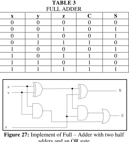
Physically, the binary signals of the inputs are considered binary digits to be added arithmetically to form a two-digit sum at output. On the other hand, the binary values are considered as variables of Boolean functions when expressed in the truth table or when the circuit is implemented with logic gates. Figure 27 shows the Implement of Full – Adder with two half adders and an OR gate.
TABLE 3
FULL ADDER
x y z C S
0 0 0 0 0
0 0 1 0 1
0 1 0 0 1
0 1 1 1 0
1 0 0 0 1
1 0 1 1 0
1 1 0 1 0
1 1 1 1 1
Figure 27: Implement of Full – Adder with two half adders and an OR gate
4.2.Analysis
Three Bit Subtraction circuit via FPGA was successfully designed and all the connection and configuration was able to communicate with each other. All the software and hardware was successfully design, simulation and testing on FPGA board. Briefly the system function will work when as the operation of subtraction started. For example 7-3=4 and the result will be show at the waveform that was generated. From the Figure 28 shows that the top module show that input output of the diagram which in the diagram, the input are a and b that both of the input are three bit. Meanwhile at the output the total sum is three bit.
Figure 28: RTL schematic for top module three bits
From Figure 29 shows that the top design of full operation and connection of three bit subtraction in design, in this design that shows the first complement in input b, and the second complement of Full Adder. In this full adder the input a and b have three bit input each of them. Meanwhile the output is three bit twos out where this output is connected to full adder to complete the operation of subtraction. E.g. 5-1=4.
Figure 29: Full RTL schematic
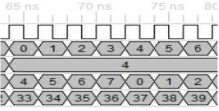
For the Figure 30 shows that operation of subtraction. Input a and b are respectively three bit. Minimum operation of subtraction could be calculated from range 0 to 7. For example a-b=total_sum. From the figure above if 3-0=3 and it will show at counter 4. If 4-1=3 it will show at counter13.
Figure 30: Simulation result of three bit subtraction
Figure 31: Simulation result of three bit subtraction
For the Figure 32 show that operation of subtraction of 5 – 4 = 1. It will show at counter 38. Any number from 0 to 7 can be calculated as input in order to do subtraction. This is because 2^(3 )=8.
Figure 32: Simulation result of three bit subtraction
5.
CONCLUSIONS
In conclusion, three bit subtraction circuit via FPGA has been successfully designed and developed. Furthermore, three bit subtraction circuit are involved in performing the subtraction for each bit by performs operation the arithmetic and logic unit, called the Arithmetic Logic Unit (ALU) example Addition, Subtraction, Multiplication and Division. The main benefit offered by the proposed system is it can simplify design the complex systems in FPGAs. In addition, the system proposed can build up more benefit to enhance better profit and minimized the human error. To have a complete system that is design by our own, one of the recommendation to enhance the possibility of this thesis is to develop the hardware equip with wireless technology. Since wireless technology is growing very fast in the modern world, it could be used in the proposed system to enhance better performance.
Acknowledgement
We are grateful to Universiti Teknikal Malaysia Melaka (UTeM) for their kind help for supplying the
electronic components and giving their laboratory facility to complete this study.
REFERENCES
[1] Steven Medina, Adders and Subtractors Design
with Verilog HDL. Fall, 2007.
[2] C. E. Cummings and S. W. B. Drive, “Correct Methods For Adding Delays To Verilog
Behavioral Models,” pp. 1–8, 1999.
[3] V. P. Orginos, “Algorithm for Multi
-operation-Logarithmic Number System
Subtraction and Addition Two Bit Compare
Four Bit,” in International Symposium On
Circuit and system, 2005, pp. 2001–2005. [4] A. Jaafar, A. H. Hamidon, A. A. Latiff, H.
Rafis, H. H. M. Yusof, and W. H. M. Saad,
“Modelling of swarm communication,”
International Journal of Advanced Research in Electrical, Electronics and Instrumentation Engineering, vol. 2, no. 8, pp. 3725–3731, 2013.
[5] Clive Maxfield, The Design Warrior’s Guide to
FPGAs: Devices, Tools and Flows. Elsevier, UK, 2004.
[6] Philip Simpson, FPGA Design: Best Practices for Team-Based Design, Third. Springer LTD, UK, 2010.
[7] Steve Kilts, Advance FPGA Design, Fourth.
John Wiley & Sons LTD, UK, 2007.
[8] N. M. Z. Hashim, M. H. A. Halim, H. Bakri,
S. H. Husin, and M. M. Said, “Vehicle Security System Using Zigbee,” International Journal of Scientific and Research Publications, vol. 3, no. 9, pp. 1–6, 2013. [9] N. M. Z. Hashim, A. F. Jaafar, Z. Zakaria, A.
Salleh, and R. A. Hamzah, “Smart Casing for Desktop Personal Computer,” International Journal Of Engineering And Computer Science (IJECS), vol. 2, no. 8, pp. 2337–2342, 2013. [10] N. M. Z. Hashim, N. A. Ali, A. Salleh, A. S. Ja,
and N. A. Z. Abidin, “Development of
Optimal Photosensors Based Heart Pulse
Detector,” International Journal of Engineering and Technology (IJET), vol. 5, no. 4, pp. 3601–3607, 2013.
[11] Samir Palnitkar, Verilog HDL: A Guide to
Digital Design and Synthesis, Second. Prentice Hall Profesional, UK., 2003.
[12] N. M. Z. Hashim, N. M. T. N. Ibrahim, Z.
Zakaria, F. Syahrial, and H. Bakri,
“Development New Press Machine using
Programmable Logic Controller,”
Computer Science (IJECS), vol. 2, no. 8, pp. 2310–2314, 2013.
[13] N. M. Z. Hashim, N. H. Mohamad, Z. Zakaria, H. Bakri, and F. Sakaguchi,
“Development of Tomato Inspection and
Grading System using Image Processing,”
International Journal Of Engineering And Computer Science (IJECS), vol. 2, no. 8, pp. 2319–2326, 2013.
[14] N. M. Z. Hashim, N. B. Hamdan, Z. Zakaria,
R. A. Hamzah, and A. Salleh, “Flood Detector Emergency Warning System,” International Journal Of Engineering And Computer Science (IJECS), vol. 2, no. 8, pp. 2332–2336, 2013. [15] P. D. Smith, David R. and Franzon, Verilog
Styles for Synthesis of Digital Systems. Prentice Hall, 2004.
[16] C. R. Mano, M. Morris and Kime, Logic and
Computer Design Fundamentals, Third. Pearson Prentice-Hall, 2004.
[17] Z. Brown, Stephen and Vranesic,
Fundamentals of Digital Logic with Verilog Design. McGraw-Hill, 2003.
[18] D. C. Hyde, “CSCI 320 Computer
Architecture Handbook on Verilog HDL,”
1997. [Online]. Available:
http://www.eg.bucknell.edu/~cs320/1995-fall/verilog-manual.html. .
[19] M. D. Ciletti, Advanced Digital Design with Verilog HDL. Prentice-Hall, 2003.
[20] H. A. A. Wahab, E. C. Tan, “CMAC Spectral