i
OPTIMIZATION OF POWER AND GAIN IN MOSFET MULTI-STAGE OPERATIONAL AMPLIFIER USING TAGUCHI’S APPROACH
NURHAZWANI BT HASHIM
This Report Is Submitted In Partial Fulfillment of Requirements for the Bachelor Degree of Electronic Engineering
(Industrial Electronic)
iii
“Saya akui laporan ini adalah hasil kerja saya sendiri kecuali ringkasan dan petikan yang tiap-tiap satunya telah saya jelaskan sumbernya .”
Tandatangan : ………..
Nama penulis : NURHAZWANI BT HASHIM
iv
“Saya/kami akui bahawa saya telah membaca karya ini pada pandangan saya/kami karya ini adalah memadai dari skop dan kualiti untuk tujuan penganugerahan Ijazah
Sarjana Muda Kejuruteraan Elektronik (Electronik Industri).”
Tandatangan : ………...
Nama Penyelia : ENGR. HAZLI RAFIS BIN ABDUL RAHIM
v
DEDICATION
vi
ACKNOWLEDGEMENT
“In the name of Allah, the most Gracious, most Powerful, and the most Merciful”
Firstly, praise to Allah SWT for guiding and blessing with perseverance and strength to complete the project. Without the strength gave to me from the God, this project report can’t be finish within the time provided. First of all, I would like to express my biggest appreciation to my beloved Project Supervisor; Engr. Hazli Rafis Bin Abdul Rahim for all his precious supports and advises during completing this project report. Furthermore, he guides me consistently and gives full dedication throughout the semester.
I also would like to thank my beloved parents especially my father and my mother for giving me the truly support and motivation to finish this project report. I am very appreciating of their understanding towards my commitment to finish the PSM report. Bundle of thanks to my friends especially to those who gave me the precious help and support in completing this project. Last but not least, I would like to thanks all the people who have involve directly and indirectly to give contribution to complete the PSM.
vii
ABSTRACT
viii
ABSTRAK
Tajuk bagi projek ini ialah pengoptimuman power dan gain dalam penguat operasional Multi-stage menggunakan kaedah Taguchi. Penguat operasional (op-amp) mempunyai nilai gain yang tinggi dan kebayakkannya digunakan dalam semua jenis alatan-alatan electronic pada masa kini. Ianya merupakan komponen asas dalam semua litar analog elektronik. Walaupun op-amp itu sendiri terdiri daripada pelbagai jenis mosfet, ia biasanya di kira sebagai satu litar yang ideal. Kecanggihan teknologi CMOS pada hari ini menyebabkan reka bentuk litar op-amp juga diubah untuk mendapatkan power dan gain yang optimum. Melalui pengurangan saiz panjang saluran mosfet, kadar
ix
TABLE OF CONTENTS
CHAPTER TITLE PAGES
PROJECT TITLE i
DECLARATION ii
DEDICATION v
ACKNOWLEDGEMENT vi
ABSTRACT vii
ABSTRAK viii
CONTENTS ix
LIST OF TABLES xi
LIST OF FIGURES xii
I INTRODUCTION
1.1 Introduction of project 1
1.12 Basic op-amp 2
1.2 Objectives of Projects 6
1.3 Project Statement 6
1.4 Scope of Projects 7
1.41 Software Design 7
1.42 Target User 7
1.5 Project Significance 8
1.6 Report Structure 8
II LITERATURE RIVIEW
2.1 Overview of Two-Stage Operational Amplifier 9
2.2 Optimization of Power 12
2.3 Taguchi Method Analysis 14
III METHODOLOGY
3.1 Project Methodology 16
3.1.1 Major project flow chart 16
3.1.2 Minor project flow chart 18
3.3 Overview of Cadence 21
3.3 Part 1: Re-design the two stage op-amp using Cadence 22
3.4 Part 2: Optimization approach 34
3.4.1 L9 (24)Array Design of Taguchi Method 36
IV RESULT AND DISCUSSION
x
4.2 Result
4.2.1 Design of Two-stage operational amplifier
38
4.2.2 Implementation of Taguchi method on 0.13 µm CMOS technology
42
4.2.2.1 Taguchi Analysis on Gain 42
4.2.2.2 Taguchi Analysis on Power Dissipation 45 4.3 Discussion
4.3.1 Confirmation Test
48
V CONCLUSION AND RECOMMENDATION
5.1 Conclusion 51
5.2 Recommendations 52
VI REFERENCES 53
xi
LIST OF TABLE
NO TITLE PAGE
1.1 Orthogonal Array 15
3.1 Specification of two stage 21
3.2 Transistor ratio 24
3.3 Value of the current 24
3.4 Process parameter and their Levels 35
3.5 Noise parameter 35
3.6 Taguchi experimental layout using L9 (24) 36
4.1 Saturated point of all transistors 39
4.2 Comparison between 0.13 µm and 0.18 µm CMOS technology 40
4.3 Gain values 42
4.4 Control factors of gain 43
4.5 Recommendable of S/N ratio of gain 43
4.7 Power dissipation values 45
4.8 Control factors of Power dissipation 46
4.9 Recommendable of S/N ratio of Power dissipation 46
4.10 Best setting of the process parameter 48
4.11 Comparison Power and Gain before and after apply Taguch i 49
xii
LIST OF FIGURE
NO TITLE PAGE
1.1 Operational Amplifier 2
1.2 Conventional op-amp topologies 3
1.3 Block Diagram 4
2.1 Two-stage Op-amp 10
2.2 Taguchi Method Procedure 13
2.3 Common orthogonal array 15
3.1 Major Project Methodology 17
3.2 Figure 3.2 Part 1 : Re-design process flow 18
3.3 Figure 3.3 Part 2: Optimization process flow 19
3.4 Figure 3.4 Cadence design tools 20
3.5 Figure 3.5 Schematic of two stage 21
3.6 Invoking cadence 25
3.7 Command Interpreter Window (CIW) 25
3.8 Library Manager 25
3.9 Virtuoso schematic window 26
3.10 Techfile 27
xiii
3.12 Adding PMOS and NMOS transistors 28
3.13 Error checking 29
3.14 DC operating point 31
3.15 AC analysis 31
3.16 Create equation for gain (dB) 32
3.17 Gain expression 32
3.18 Gain 33
3.19 Setting power expression 33
4.1 Design of two-stage operational amplifier 38
4.2 Gain of 0.13 µm and 0.18 µm CMOS technology 40
4.3 Chart of the each factors 44
4.4 Pareto chart of % factor effects on S/N ratio 46
4.5 Chart of the each factors 47
4.6 Pareto chart of % factor effects on S/N ratio 47
xiv
LIST OF APPENDIXES
NO TITLE PAGE
1 APPENDIX A 56
1
CHAPTER 1
INTRODUCTION
Chapter 1 covers about the introduction part of this Final Year Project of Degree. It contains subchapter of objectives, problem statements, scopes of project and project significance.
1.1Introduction of Project
2
The common IC operational amplifier is one which has very high gain and finds widespread use in many electronics. Its application is not limited to linear amplification system, but includes digital logic system as well. A common IC takes the form of an operational-amplifier (op-amp) which provides various choices in its applications e.g. the input can be either or non-inverting.
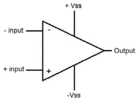
[image:16.612.268.409.301.401.2]Similarly, op-amp can be used as differential amplifiers in which the output signal is proportional to the difference of two input signals. It is quite usual that a single amplifier cannot provide the gain which we desire. We therefore use two or more cascode amplifier.
Figure 1.1 Operational amplifier
1.12 Basic op-amp
There are several of op-amp exist in basic literature, each having the positive and negative aspects in terms of performances. Below are few types of op-amp:
I. Telescopic amplifier II. Folded cascode amplifier III. Two stage amplifier
3
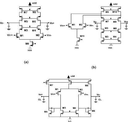
(a)
[image:17.612.120.535.71.465.2](b)
Figure 1.2 Conventional op-amp topologies (a) Telescopic amplifier (b) Folded-cascade amplifier (c) Two-stage amplifier
A. Telescopic amplifier
It is simply similar to differential amplifier but typically has higher frequency and consumes less power than other topologies. It is extension of differential amplifier where input and load are replaced by cascode pairs so as to increases the gain of the output given as:
Av = gm1 [(gm3.ro3.ro1)|| (gm5.ro5.ro7)]
Even it has high gain, this amplifier is not used due to its small voltage swing which is controlled by the overdrive voltage of cascode.
4
B. Folded cascode amplifier
It is used quite widely compare to telescopic topologies, because of the input and outputs can be shorted together and the choice of the input common-mode level is easier. This amplifier is used to increase the output swing by folds the input transistor to either to Vdd or ground and two tail current sources. The gain is:
Av = gm1 {[(gm3.ro3.(ro1|| ro5)] || [gm7.ro7.ro9]}
C. Two-stage amplifier
A single stage has low frequency gain which is Av = gm1 (ro1 || ro3)
[image:18.612.256.472.432.485.2]compare to two-stage amplifier. It can gives good gain but lesser in swing output. Hence, the two-stage can be designed in such that the gain and swing are independent. At the first stage, it can provide a high gain whereas at second stage it can gives a high swing and each can be controlled independently.
Figure 1.3 Block Diagram
Av, first stage = gm1,2(ro1,2 || ro3,4)
Av, second stage = gm5,6(ro5,6 || ro7,8)
Overall gain Av = Av, first stage × Av, second stage
5
provide higher caliber of quality in products and accommodations for incrementing market continue competitively among the manufacturers to ascertain customer gratification. Optimization is needed as it result in better performances and reducing cost. After all, optimizing the parameters has become mandatory now a day in operational amplifier design.
There are a lot of methods have been developed to optimize parameters in a circuit to achieve high gain and low power such as
I. Geometric Programming II. Gain-Boosted Op-Amp (GBO) III. Taguchi Method
The feature of geometric programs introduced new method for determining components values an transistor dimensions for CMOS op-amp. It can be used to synthesize robust design that is design guaranteed to meet the specifications for a variety of process conditions and parameters. [2]
The methodology of gain-boosted op-amp (GBO) allows the optimization in terms of ac response and settling performance and is incorporated into an automatic computer-aided design (CAD) tool, called GBOPCAD. [3]
Taguchi method is based on statistical approach and it will be used to optimize selected parameters such as W/L ratio of transistors, chopping frequency, size of chopper modulator and bias current to achieve low noise and low offset. [4]
6
1.2Objective of Project
The main objective of this study is to optimize power and gain in MOSFET multi-stage op-amp. This objective is supported by the following sub objectives:
I. To design new multi-stage op-amp
II. To investigate the performances of Multistage using CMOS 0.13 µm, 0.18 µm and 0.2 µm technology.
III. To apply Taguchi method on the best CMOS technology
1.3Problem Statement
Designing high-performance analog circuits is crucially important and challenging with the insistent trend toward reduced supply voltages. Operational amplifier is used in this project due to it offers good voltage gain, good common mode range and good output swings. Nevertheless, there are few problems arise within those topologies, some have a very high gain but less speed and swing, some have good speed but the gain is imbalance. From the background research, two-stage operational amplifier gives the better output compare to others topologies because gain and swing can be control independently.
7
1.4Scope of Project
The scope of this study had been identified. The problem characteristics will be on; I. The investigation of two stage op-amp using the Taguchi approach.
II. Redesign and simulate the circuit by using the Cadence software and until the schematic result with layout.
III. Analyze the performance of op-amp based on CMOS technology
1.4.1 Software Design
This project focuses on the redesign circuit using Cadence software. It is an essential role in the creation of today’s electronics such as software, hardware and expertise to verify today’s mobile. In short it is tools for designing full-custom integrated circuits of operational amplifier.
1.4.2 Target User
8
1.5 Project Significance
The optimization of power and gain will improve the modeling accuracy for sub-micron technologies especially in operational amplifier. Hence, the new modeling design of multi stage op-amp will optimize power and gain such as in signal processing circuit and instrumentation. As for Taguchi method, it is an efficient problem solving tools which can improve the performance of the product, process design, and system with the experimental time and cost.
1.5Report Structure
The report consists of five chapters which is Chapter 1 will discusses about the introduction of the project which includes the objectives of the project, problem statements, scope of the project, project significance and report structure. The problem statement describes the problem that faced by the performance of each topologies and follow by the discussion of the scope and significance of the project.
Chapter 2 is discussed about Literature review. The first part is about the importance of optimization in power and gain in each device. Then, analyze the effect of redesign two-stage operational amplifier and the process involving Taguchi method.
The next chapter, chapter 3 discusses about Project Methodology of the project. The methodology involved system analysis, system design, and system testing.
Then, chapter 4 discusses about Result and Discussion of the project. It is about result full decision after the completion of this project.
9
CHAPTER 2
LITERATURE REVIEW
This chapter presents an overview of the previous works on the related topic for providing the background of this study.
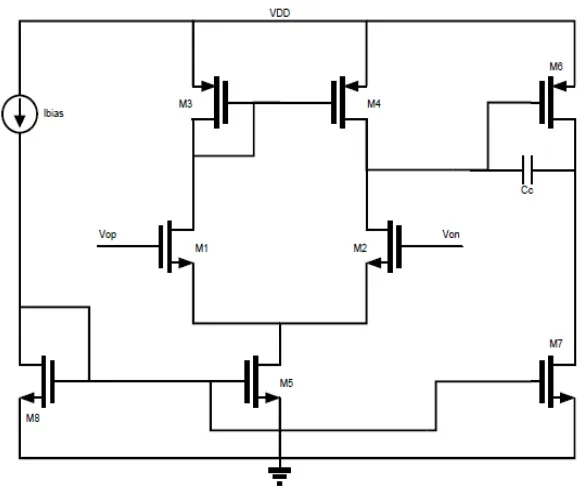
2.1 Overview of two-stage operational amplifier
Two stage op-amp consists of a cascade of V to I and I to V stages [5]. It is divided into two parts; first stage and two stage as shown in Figure 2.1. The first stage consists of a differential amplifier which is convert the differential input voltages to differential currents. These differential currents are applied to a current-mirror load by replacing the differential voltage [7]. This is known as differential voltage amplifier. The second stage consists of a common-source MOSFET that convert the second stage input voltage to current known as current-sink inverter. This two stage op-amp is so widely used in current technology
10
Figure 2.1 Two-stage op-amp
Node 1 forms the output of the first stage of the op amp. The second stage consists of M6 which is a common-source amplifier actively loaded with the transistor M7. The transistor M7 does not provide biasing for M6, instead M6 is biased from the gate side. The capacitor CC known as Miller compensation is to increase the phase margin of the system [6]. The design parameters of the two stage op-amp are discussed below:
I. The minimum value for the tail current (I5) from the largest of the two values is determined.
I5 =SR.Cc
I5 is nearly equal to
S SS DD
T V V
2
|) | (