MICRO HOLE DRLLING BY INDUSTRIAL CO2 LASER
MOHD KAMAL BIN MOHD KASIM
B051010151
UNIVERSITI TEKNIKAL MALAYSIA MELAKA
UNIVERSITI TEKNIKAL MALAYSIA MELAKA
This report submitted in accordance with requirement of the Universiti Teknikal Malaysia Melaka (UTeM) for the Bachelor Degree of Manufacturing Engineering
(Manufacturing Process) (Hons.)
by
MOHD KAMAL BIN MOHD KASIM B051010151
910428-06-5079
FACULTY τF MAσUFACTURIσG EσGIσEERIσG 2014
UNIVERSITI TEKNIKAL MALAYSIA MELAKA
BORANG PENGESAHAN STATUS LAPORAN PROJEK SARJANA MUDA
TAJUK: Micro Hole Drilling by Industrial CO2 Laser SESI PENGAJIAN: 2013/14 Semester 2
Saya MOHD KAMAL BIN MOHD KASIM
mengaku membenarkan Laporan PSM ini disimpan di Perpustakaan Universiti Teknikal Malaysia Melaka (UTeM) dengan syarat-syarat kegunaan seperti berikut:
1. Laporan PSM adalah hak milik Universiti Teknikal Malaysia Melaka dan penulis. 2. Perpustakaan Universiti Teknikal Malaysia Melaka dibenarkan membuat salinan
untuk tujuan pengajian sahaja dengan izin penulis.
3. Perpustakaan dibenarkan membuat salinan laporan PSM ini sebagai bahan
pertukaran antara institusi pengajian tinggi.
4. **Sila tandakan ( )
SULIT
TERHAD
TIDAK TERHAD
(Mengandungi maklumat yang berdarjah keselamatan atau kepentingan Malaysia sebagaimana yang termaktub
DECLARATION
I hereby, declared this report entitled “Micro Hole Drilling by Industrial Cτ2 Laser" is the results of my own research except as cited in references.
Signature μ ……….
Author’s σame μ Mohd Kamal Bin Mohd Kasim
APPROVAL
This report is submitted to the Faculty of Manufacturing Engineering of UTeM as a partial fulfillment of the requirements for the degree of Bachelor of Manufacturing Engineering (Manufacturing Process) (Hons). The member of the supervisory is as followμ
………..
i
1.
ABSTRAK
Pemesinan Laser adalah salah satu kemajuan pemesinan yang paling popular di dunia ini. Pada masa kini, pemesinan micro laser digunakan dalam pengeluaran MEMS untuk mengambil alih kaedah tradisional seperti proses punaran yang memerlukan tempoh masa untuk menyelesaikan proses tersebut. τbjektif kajian ini adalah untuk menyiasat keupayaan penggerudian laser industri, laser Cτ2, dalam pemprodedan
silikon wafer. Dalam karya ini, lubang-lubang digerudi pada wafer silikon jenis-P
dengan ketebalan 525 m dan 100 mm diameter. Lubang-lubang diperhatikan dengan
ii
2.
ABSTRACT
Laser machining is one of the most popular advance machining in this world. σowadays, laser micromachining is currently used in the MEMS production to take over the traditional method such as etching process that needs a period of time to finish the process. The objective of this study is to investigate the drilling capability of industrial laser, Cτ2 laser, in silicon wafer processing. In this work, the holes were
drilled on P-type silicon wafer with thickness 525 µm and 100 mm diameter. The
iii
DEDICATION
To my beloved father and mother
iv
3.
ACKNOWLEDGEMENT
vi
2.11 Laser Parameter 25
2.11.1 Laser Power 26
2.11.2 Pulse Frequency 26
2.11.3 Duty Cycle 27
2.12 Entrance Diameter (dentrance) 27
2.13 Silicon Surface Preparation 28
4.2 Investigation of Entrance Diameter of Drilling Holes 48
4.3 Experimental Result of Laser Drilling Process 48
vii
4.4.1 τptimization 56
4.5 The Spatter Deposition Area of Laser Drilling Hole 58
CHAPTER 5 : CONCLUSION 61
5.1 Conclusion 61
5.2 Recommendation 62
6. APPENDIX A 70
7. APPENDIX B 73
viii
4.
LIST OF FIGURES
2.0μ Micromotor as one of the MEMS product 5
2.1μ Basic formation of laser λ
2.2μ Electromagnetic spectrum wavelength for several laser types λ
2.3μ Absorption mechanism 10
2.10μ Difference number of cycle that produce in one second 26
2.11μ Laser pulse 27
2.12μ Measuring process of hole diameter on silicon wafer 28
3.0μ Research flow chart 31
3.1μ Central composite design 35
3.2μ Box-behnken design for three factors 35
3.3μ Experimental parameters setup 37
3.4μ Experiment response setup 37
3.5μ Table of run for experiment 38
3.6μ Laser cutting machine (Helius 2513) 3λ
3.7μ The experimental setup flow chart 40
3.8μ AUTτCAD drawing for the laser drilling process 42
3.λμ Schematic diagram of Cτ2 laser micromachining setup 43
3.10μ Laser beam nozzle 43 3.11μ X and Y direction of drilling hole 45
ix
4.0μ Drilled hole on a silicon wafer 47
4.1μ The experimental value and predicted value of dentrance 52
4.2μ Effects of Laser power to the dentrance of drilling holes 53
4.3μ Effects of pulse frequency to the dentrance of drilling holes 54
4.4μ Effects of duty cycle on the dentrance of drilled hole 55
4.5μ Interaction of laser power and pulse frequency to the dentrance 56
4.6μ Suggested parameter value of laser drilling process 57
4.7μ Predicted entrance diameter of drilling hole 58
x
5.
LIST OF TABLES
2.0μ Types of laser with wavelength and average power range. 16
2.1μ Typical carbon dioxide (Cτ2) laser parameters. 18
2.2μ Standard on silicon wafer sizes and thickness. 21
2.3 (a)μ Mechanical properties of silicon. 22
2.3 (b)μ Thermal properties of silicon 22
2.4μ Laser input and output parameters 23
2.5μ Frequency for laser input and output parameters 24
2.6μ Descend order of input and output laser parameters 24
2.7μ Summary of laser input and output parameters 25
3.0μ Parameter used for experiment 33
3.1μ Basic specification of laser machine Helius - 2531 3λ
4.0μ Experiment run and test result for laser drilling process 4λ
4.1μ Experiment result after run eliminating process 50
4.2μ Table of AστVA for dentrance holes 51
4.3μ τptimization solution proposed by Design Expert 57
xi
6.
LIST OF SYMBOLS
mm - Millimetre
nm - nanometer
In - Inch
W - Watt
KW - Kilowatt
oC - Celcius
µ - Micron, 1 x 10⁻⁶
Hz - Hertz
% - Percent
σ - σitrogen
τ2 - τxygen
Cτ2 - Carbon Dioxide
1
1.
CHAPTER 1
INTRODUCTION
1.1 Introduction
This chapter explains about several sections which include the background of study, problem statements, research objectives, research scope and completed by limitations of research.
1.2 Background of Study
In the world today, the manufacturing industries need advanced machining techniques to follow the rigorous design requirement and to machine the hard-to
-machine material such as titanium, steel, super alloy materials, composite and ceramics. Laser machining is one of the most popular advances machining in this world. Lasers are broadly applied in industry as cutting tools due to ultra-flexibility of the cutting conditions, quick set up, obtaining a high quality end product, the small size of the heat affected zone, and non-mechanical contact between the workpiece and the tool (Yilbas, 2004).
There are a lot of laser resource types that commonly used in manufacturing industries and the current types of laser used are Cτ2 and σdμ YAG laser. σearly λ0
percent of all industrial laser material processing used both types of lasers. Basically, both types of laser have different capabilities cut or drill a piece of materials by
2
electronics, aerospace, biomedical, MEMS, and other applications because it provides rapid, precise, clean, flexible, and efficient process (Han et al, 2004).
Micro-electromechanical system (MEMS) is a technology used to create small
integrated devices or systems that merges mechanical and electrical components. This technology has abilities to sense, control and actuate on the micro scale, and generate effects on the macro scale. There are four types of MEMS component which is micro sensors, micro actuators, microelectronics and microstructure. The primary material used in MEMS is Silicon (Jiang et al, 200λ). MEMS application includes the process control and automation, automotive industry, scientific and medical instrumentation, and telecommunication.
1.3 Problem Statement
In recent year, majority of MEMS manufacturing companies likes to use σdμ YAG laser for drilling micro hole on the silicon wafer. By applying σdμ YAG lasers which produce short pulses and the UV wavelength, this permit a reduction of thermal effects like heat affected zones (HAZ) and deposition of molten material at the cutting edge (Klozbach.U et al, 2011).
The wavelength of a Cτ2 laser is 10.64 m and not absorbed by silicon material
(Chung et al, 2006). Silicon is not an active optical material. This material is only effective in detecting light and the emission of light is difficult to achieve. So, this is difficult to apply the drilling technique by using Cτ2 laser because this laser
provides a long pulse and wavelength that cannot absorb by silicon material.
Cτ2 laser is typically used to drill holes larger than 100 m in diameter and cannot
drill holes smaller than 75 m (Luziusa et al, 2013). Furthermore, there is still less research done regarding the laser drilling process on a silicon wafer by using Cτ2
3
material will have different properties that allowed the laser move throughout the material.
This project is about the experimental studies of the micro laser drilling of silicon wafers by using Cτ2 laser. Laser parameters such as laser power, pulse frequency,
and duty cycle will be set up to drill holes on 525 µm thickness of silicon wafers. Entrance diameter of drilling holes will be analyzed. This project results will provide a common advice in generating micro holes on the MEMS structure on silicon wafers using Cτ2 laser.
1.4 Objectives of the Research
The objectives of this research are toμ
i. Investigate the drilling capability of Cτ2 laser in silicon wafer processing. ii. Model the laser processing of silicon wafer.
iii. τptimize the develop model.
1.5 Scope of the Study
This research will be conducted by using Helius 2513 Laser Cutting Machine with rated power of 3000 watts. P-types silicon wafer with 525 µm thickness and 100 mm
4
2.
CHAPTER 2
LITERATURE REVIEW
2.1 Introduction
In this chapter, the research review is focused on several main sections such as the Micro Electro Mechanical System (MEMS), types of machine and material, and the methods used to design an experiment. This information is useful so that appropriate parameters of laser machining can be chosen based on previous research, in order to drill silicon wafer.
2.2 Micro Electro Mechanical System (MEMS)
Micro-electromechanical system or known as MEMS is one of the process
technology applied to produce smaller devices or systems that bring together the electrical and mechanical components. In the United States, the technology is known as micro-electromechanical system (MEMS) but in Europe, it is known as
5
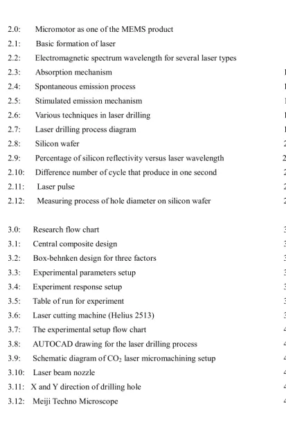
Figure 2.0μ Micromotor as one of the MEMS product (Hsu 2002).
This technology basically made up using integrated circuit (IC) and can be in several of sizes from a few micrometres to millimeters. MEMS contains components of sizes in ranges of 1 micrometer to 1 milimeter (σadim Maluf, 2004). MEMS are a developing technology which applies integrated circuit (IC) fabrication methods to create integrated microsensor, microactuators, and microelectronics to make micron size devices which can sense and act on the local environment (Simon, 2010). There
were several types of MEMS components which consisting of mechanical
microstructures, microsensors, microactuators and microelectronics. All of this form was integrated onto the same silicon chip.
2.2.1 Application of MEMS
σowadays, MEMS is an unknown and famous technology used in the world. Smartphone industries are not neglecting to apply MEMS in producing new models of Smartphone. Smart phones were generally provided with tri-axis magnetometer
and tri-axis MEMS accelerometer such as the start adding tri-axis MEMS gyroscope,
6 MEMS technology also has been used in the automotive sectors in term of sensors. There were above 100 sensors used involving gyroscopes for higher fuel efficiency, MEMS Tire Pressure Monitoring System (TPMS) and other purposes (Chun et al, 2012). For the Electronic Stability Program (ESP) or vehicle dynamic system (VDC), this system was the most effective active safety systems in the automotive domain, supporting the driver to retain the vehicle on the intended path, thus helping to avoid accidents (Marek, 2011). The MEMS technology also can help in the vehicle fuel consumption. The vehicle based pressure sensors such as manifold
pressure sensor are used to determine the air intake of the engine. With the help of a barometric pressure sensor, combustion algorithms can be adjusted in correlation with the ambient air pressure (Finkbeiner, 2007).
For the medical sectors, accelerometers and pressure sensors remain the largest two market segments for MEMS products and technology. These components can be applied to determine the human blood pressure accurately only in several second time. For the efficiency of computer using in medical application, MEMS accelerometers and fiber optic sensors have produced as an interface between a user and a computer. The movement of user's body can be measured directly by wearing these types of sensors. In the biomedical application, optical MEMS also have been applying in multifunctional endoscope that used for advanced diagnosis and endoscopic surgery (Miyajima, 2002).
2.2.2 Fabrication of MEMS
Laser micromachining of dielectrics and metals is a multipurpose fabrication and repair tool for applications in MEMS, microelectronics, and micro-fluidics,
7 Bulk micromachining is a process of removal of material from the bulk substrates to form the desired three dimensional geometry of the microstructure. This is
sometimes done to “undercut” structures that compulsory to physically move which is to produce membranes on one side of a wafer and to make a mixture of trenches, holes, or other structures. These types of micromachining basically consist of several
techniques which is wet etchant and dry etchant.
Then in the surface micromachining technique, the material is removed by physical or chemical means and the micromachining surface will build microstructure by adding material layer by layer on top of the substrate. Surface micromachining technique many benefits which a low-cost technique, batch-manufacturing process, and can achieve much higher alignment accuracy than is possible by conventional passive-alignment techniques.
In the LIGA process, this process begins with deep x-ray lithography that sets the
desired pattern of a thick film of photoresist. After the substrates and photoresists material have been chosen, the electroplating process will be done. In many micromachining technologies, photolithography techniques are used to transfer the desired pattern from a mask to the structural material. As one of the cheapest and most capable surface-micromachining processes, LIGA has concerned much attention for millimeter-wave and microwave device (Yun et al, 2002).
2.3 Laser Micromachining
8 Different issues when used laser micromachining to replace the traditional etching process that result will be faster, accurate and high production rate. The application areas of laser micro machining involved of manufacturing methods like cutting, drilling, welding as well as ablation and material surface texturing, whereby it is possible to get a very fine surface structure ranging in the micrometer domain (Klozbach. U et al, 2011). The established laser micromachining method has minimized normal problems in laser micromachining such as the laser polarization effect, material recast (microcracks to the sidewall of structures), and Heat Affected Zone (HAZ), (Zhu et al, 2002).
There were many types of lasers used in the laser micromachining process. There are from microsecond pulsed infrared Cτ2 gas laser at a wavelength between λ.3-11µm
to nanosecond pulsed excimer gas laser in the 157-353 µm UV wavelength range. In
silicon etching process, Cτ2 laser with wavelength 10.64 m have been used with glass attached to the Si backside because the pure silicon cannot absorb the laser wavelength (Chung et al, 2006).
The increasing of the laser pulse is continuing from Femto-second to nanosecond
pulsed solid state laser between wavelengths of 266 - 1060 σM. A micro-structuring of SiO2 thin film on Si have been applied by using Femto-second laser pulse with 150 femtosecond pulse duration and a maximum energy up to 3mJ/pulse. Actually, all of the laser types are used depending on the types of material to be processed.
2.4 Fundamental principle of Laser