LAMPIRAN
$regfile = "m8535.dat"
$crystal = 4000000
Config Adc = Single , Prescaler = Auto , Reference = Avcc
Config Lcdpin = Pin , Rs = Portb.0 , E = Portb.1 , Db4 = Portb.2 , Db5 = Portb.3 , Db6 = Portb.4 , Db7 = Portb.5
Config Lcd = 20 * 4
Dim Suhulm35 As Word , Probepeha As Word , Suhu As Single , Lm35 As Byte
Dim Samples As Word , Maks As Word , Minm As Word , I As Byte , This_sample As Word , Diff As Word
Dim Pehaakhir As Single , Pengali As Single , Nilaipeha As Byte , Cekph As Single
Dim Karakter1 As String * 6
Dim Karakter2 As String * 6
Dim Detik As Integer , Menit As Integer , Jam As Integer
Dim Hari As Integer , Bulan As Integer , Tahun As Integer
Dim Weekday As Byte
Const Ds1307w = &HD0 ' Addresses of Ds1307 clock
Config Sda = Portc.1
Config Scl = Portc.0
Config Clock = User
Ddrd.4 = 1
Ddrd.5 = 1
Pompa_asam Alias Portd.4
Pompa_basa Alias Portd.5
Ddrc.2 = 0
Ddrc.3 = 0
Level_asam Alias Pinc.2
Level_basa Alias Pinc.3
Ddrc.4 = 1
Buzzer Alias Portc.4
Ddrc.5 = 1
Ddrc.6 = 1
Led_level_asam Alias Portc.5
Led_level_basa Alias Portc.6
Dim Tampung As Word , Liter As Byte , Limit_put As Word
Dim Tampung2 As Word , Liter2 As Byte , Limit_put2 As Word
Cursor Off
Cursor Noblink
'default 1 = OFF --> low active
Led_level_asam = 1
Led_level_basa = 0
'default 1 = OFF --> low active
Buzzer = 1
Config Int0 = Rising
Config Int1 = Rising
'Set up timer to track time
Config Timer1 = Timer , Prescale = 256
Stop Timer1
'Preload Timer Constant For 1 Second Duration At 4 Mhz for 256 prescale
Const Timer1pre = 49911
Timer1 = Timer1pre
'Handle time overflow (occurs every second)
On Timer1 Pulse
Start Timer0
Start Timer1
Enable Interrupts
Enable Timer1
Enable Int0
Enable Int1
On Int0 Hitung
On Int1 Hitung2
Led_level_asam = 1
Led_level_basa = 1
Buzzer = 1
Cls
Cursor Off
Cursor Noblink
Tampung = 0
Tampung2 = 0
Liter = 0
Limit_put = 0
Dim Cek_peha As String * 5
'_sec = 0
'_min = 50
'_hour = 17
'Wait 1
'Gosub Settime
'_sec = 14
'_min = 59
'_hour = 7
'Gosub Clock_init
'Wait 1
'Gosub Settime
Const 1putaran = 150
Limit_put = 1000
' 1 --> pump OFF
Pompa_asam = 1
Pompa_basa = 1
Dim Mmenit As Byte
Mmenit = 0
Utama:
Do
Locate 1 , 1
Lcd "Monitoring pH System"
Gosub Disply_seting
Deflcdchar 0 , 6 , 9 , 9 , 6 , 32 , 32 , 32 , 32
Locate 3 , 1
Lcd "LM35:" ; Lm35 ; Chr(0) ; "C " ; "| pH:" ; Karakter2 ; " "
'Lcd "Count:" ; Tampung ; " " ; "Nilai:" ; Liter ; " "
Gosub Cek_sensor_peha
Gosub Cek_level_liquid
'utk debug saja
Locate 2 , 16
Lcd Mmenit
Locate 4 , 1
'Lcd "pH Real:" ; Pehaakhir
If Mmenit = 2 Then
Mmenit = 0
Gosub Scan_pompa_asam
Cls
End If
If Detik = 0 Then 'realnya detik diganti menit
Wait 1
Incr Mmenit
End If
Waitms 200
End
Cek_level_liquid:
If Level_asam = 1 Or Level_basa = 1 Then
Buzzer = Not Buzzer
Waitms 500
Buzzer = 1
End If
If Level_asam = 1 Then
Led_level_asam = Not Led_level_asam
Waitms 100
Led_level_asam = 1
Else
Led_level_asam = 1
End If
If Level_basa = 1 Then
Led_level_basa = Not Led_level_basa
Waitms 100
Led_level_basa = 1
Else
Led_level_basa = 1
End If
Return
Cls
Waitms 100
If Pehaakhir >= 6.79 And Pehaakhir <= 6.95 Then
Buzzer = 0
Waitms 100
Buzzer = 1
Do
Pompa_asam = 0
Locate 1 , 1
Lcd "Monitoring pH System"
Gosub Lm35
Gosub Disply_seting
Gosub Cek_sensor_peha
Deflcdchar 0 , 6 , 9 , 9 , 6 , 32 , 32 , 32 , 32
Locate 3 , 1
Lcd "LM35:" ; Lm35 ; Chr(0) ; "C " ; "| pH:" ; Karakter2 ; " "
Locate 4 , 1
Lcd "Pulse: " ; Tampung ; " "
Loop Until Tampung >= 4565
Pompa_asam = 1
Tampung = 0
Goto Utama
End If
If Pehaakhir >= 6.59 And Pehaakhir <= 6.78 Then
Buzzer = 0
Buzzer = 1
Do
Pompa_asam = 0
Locate 1 , 1
Lcd "Monitoring pH System"
Gosub Lm35
Gosub Disply_seting
Gosub Cek_sensor_peha
Deflcdchar 0 , 6 , 9 , 9 , 6 , 32 , 32 , 32 , 32
Locate 3 , 1
Lcd "LM35:" ; Lm35 ; Chr(0) ; "C " ; "| pH:" ; Karakter2 ; " "
Locate 4 , 1
Lcd "Pulse: " ; Tampung ; " "
Loop Until Tampung >= 5375
Pompa_asam = 1
Tampung = 0
Goto Utama
End If
If Pehaakhir >= 6.39 And Pehaakhir <= 6.58 Then
Buzzer = 0
Waitms 100
Buzzer = 1
Do
Pompa_asam = 0
Locate 1 , 1
Gosub Lm35
Gosub Disply_seting
Gosub Cek_sensor_peha
Deflcdchar 0 , 6 , 9 , 9 , 6 , 32 , 32 , 32 , 32
Locate 3 , 1
Lcd "LM35:" ; Lm35 ; Chr(0) ; "C " ; "| pH:" ; Karakter2 ; " "
Locate 4 , 1
Lcd "Pulse: " ; Tampung ; " "
Loop Until Tampung >= 11000
Pompa_asam = 1
Tampung = 0
Goto Utama
End If
If Pehaakhir >= 6.19 And Pehaakhir <= 6.38 Then
Buzzer = 0
Waitms 100
Buzzer = 1
Do
Pompa_asam = 0
Locate 1 , 1
Lcd "Monitoring pH System"
Gosub Lm35
Gosub Disply_seting
Gosub Cek_sensor_peha
Deflcdchar 0 , 6 , 9 , 9 , 6 , 32 , 32 , 32 , 32
Lcd "LM35:" ; Lm35 ; Chr(0) ; "C " ; "| pH:" ; Karakter2 ; " "
Locate 4 , 1
Lcd "Pulse: " ; Tampung ; " "
Loop Until Tampung >= 12500
Pompa_asam = 1
Tampung = 0
Goto Utama
End If
'=============================================================
'basa
If Pehaakhir >= 7.5 And Pehaakhir <= 7.6 Then
Buzzer = 0
Waitms 100
Buzzer = 1
Do
Pompa_basa = 0
Locate 1 , 1
Lcd "Monitoring pH System"
Gosub Lm35
Gosub Disply_seting
Gosub Cek_sensor_peha
Deflcdchar 0 , 6 , 9 , 9 , 6 , 32 , 32 , 32 , 32
Locate 3 , 1
Lcd "LM35:" ; Lm35 ; Chr(0) ; "C " ; "| pH:" ; Karakter2 ; " "
Locate 4 , 1
Loop Until Tampung2 >= 2000
Pompa_basa = 1
Tampung2 = 0
Goto Utama
End If
If Pehaakhir >= 7.61 And Pehaakhir <= 7.7 Then
Buzzer = 0
Waitms 100
Buzzer = 1
Do
Pompa_basa = 0
Locate 1 , 1
Lcd "Monitoring pH System"
Gosub Lm35
Gosub Disply_seting
Gosub Cek_sensor_peha
Deflcdchar 0 , 6 , 9 , 9 , 6 , 32 , 32 , 32 , 32
Locate 3 , 1
Lcd "LM35:" ; Lm35 ; Chr(0) ; "C " ; "| pH:" ; Karakter2 ; " "
Locate 4 , 1
Lcd "Pulse: " ; Tampung2 ; " "
Loop Until Tampung2 >= 3000
Pompa_basa = 1
Tampung2 = 0
Goto Utama
If Pehaakhir >= 7.71 And Pehaakhir <= 7.8 Then
Buzzer = 0
Waitms 100
Buzzer = 1
Do
Pompa_basa = 0
Locate 1 , 1
Lcd "Monitoring pH System"
Gosub Lm35
Gosub Disply_seting
Gosub Cek_sensor_peha
Deflcdchar 0 , 6 , 9 , 9 , 6 , 32 , 32 , 32 , 32
Locate 3 , 1
Lcd "LM35:" ; Lm35 ; Chr(0) ; "C " ; "| pH:" ; Karakter2 ; " "
Locate 4 , 1
Lcd "Pulse: " ; Tampung2 ; " "
Loop Until Tampung2 >= 4000
Pompa_basa = 1
Tampung2 = 0
Goto Utama
End If
If Pehaakhir >= 7.81 And Pehaakhir <= 7.9 Then
Buzzer = 0
Waitms 100
Do
Pompa_basa = 0
Locate 1 , 1
Lcd "Monitoring pH System"
Gosub Lm35
Gosub Disply_seting
Gosub Cek_sensor_peha
Deflcdchar 0 , 6 , 9 , 9 , 6 , 32 , 32 , 32 , 32
Locate 3 , 1
Lcd "LM35:" ; Lm35 ; Chr(0) ; "C " ; "| pH:" ; Karakter2 ; " "
Locate 4 , 1
Lcd "Pulse: " ; Tampung2 ; " "
Loop Until Tampung2 >= 4000
Pompa_basa = 1
Tampung2 = 0
Goto Utama
End If
If Pehaakhir >= 7.91 And Pehaakhir <= 8.0 Then
Buzzer = 0
Waitms 100
Buzzer = 1
Do
Pompa_basa = 0
Locate 1 , 1
Lcd "Monitoring pH System"
Gosub Disply_seting
Gosub Cek_sensor_peha
Deflcdchar 0 , 6 , 9 , 9 , 6 , 32 , 32 , 32 , 32
Locate 3 , 1
Lcd "LM35:" ; Lm35 ; Chr(0) ; "C " ; "| pH:" ; Karakter2 ; " "
Locate 4 , 1
Lcd "Pulse: " ; Tampung2 ; " "
Loop Until Tampung2 >= 5000
Pompa_basa = 1
Tampung2 = 0
Goto Utama
End If
Cls
Return
Pulse:
Stop Timer0
Stop Timer1
Counter0 = 0
Timer1 = Timer1pre
Start Timer0
Start Timer1
Return
Incr Tampung
Return
Hitung2:
Incr Tampung2
Return
Lm35:
Suhulm35 = Getadc(0)
Suhu = Suhulm35 * 5
Suhu = Suhu / 1024
Suhu = Suhu * 100
Lm35 = Suhu
Return
Cek_sensor_peha:
Samples = 2000
Maks = 0
Minm = 1024
For I = 0 To Samples Step 1
Probepeha = Getadc(1)
If Probepeha > Maks Then
Maks = Probepeha
Elseif Probepeha < Minm Then
Minm = Probepeha
End If
Next I
Pehaakhir = -0.029 * Maks
Pehaakhir = Pehaakhir + 21.1
'Pehaakhir = Pehaakhir
Nilaipeha = Pehaakhir
Karakter2 = Fusing(pehaakhir , "#.#") ' y = -0.03x + 22
Return
Disply_seting:
Gosub Getdatetime
Jam = _hour
Menit = _min
Detik = _sec
Locate 2 , 5
If Jam < 10 Then
Lcd "0" ; Jam ; ":" ;
Else
Lcd Jam ; ":" ;
End If
If Menit < 10 Then
Else
Lcd Menit ; ":" ;
End If
If Detik < 10 Then
Lcd "0" ; Detik
Else
Lcd Detik
End If
Return
Getdatetime:
I2cstart
I2cwbyte Ds1307w
I2cwbyte 0
I2cstart
I2cwbyte Ds1307r
I2crbyte _sec , Ack
I2crbyte _min , Ack
I2crbyte _hour , Ack
I2crbyte Weekday , Ack
I2crbyte _day , Ack
I2crbyte _month , Ack
I2crbyte _year , Nack
I2cstop
_sec = Makedec(_sec) : _min = Makedec(_min) : _hour = Makedec(_hour)
Return
Settime:
_sec = Makebcd(_sec) : _min = Makebcd(_min) : _hour = Makebcd(_hour)
I2cstart
I2cwbyte Ds1307w
I2cwbyte 0
I2cwbyte _sec
I2cwbyte _min
I2cwbyte _hour
I2cstop
Return
Setdate:
_day = Makebcd(_day) : _month = Makebcd(_month) : _year = Makebcd(_year)
I2cstart
I2cwbyte Ds1307w
I2cwbyte 4
I2cwbyte _day
I2cwbyte _month
I2cwbyte _year
I2cstop
Return
Clock_init:
I2cstart
I2cwbyte &H00
I2cwbyte &H00 And &B01111111
I2cstop
I2cstart
I2cwbyte Ds1307w
I2cwbyte &H07
I2cwbyte &B10010000
I2cstop
1/7
®
BTA/BTB12 and T12 Series
SNUBBERLESS™, LOGIC LEVEL & STANDARD
12A TRIAC
S
September 2000 - Ed: 3
MAIN FEATURES:
DESCRIPTION
Available either in through-hole or surface-mount packages, the BTA/BTB12 and T12 triac series is suitable for general purpose AC switching. They can be used as an ON/OFF function in applications such as static relays, heating regulation, induction motor starting circuits... or for phase control operation in light dimmers, motor speed controllers,...
The snubberless versions (BTA/BTB...W and T12 series) are specially recommended for use on inductive loads, thanks to their high commutation performances. By using an internal ceramic pad, the BTA series provides voltage insulated tab (rated at 2500V RMS) complying with UL standards (File ref.: E81734)
Symbol Value Unit
IT(RMS) 12 A
VDRM/VRRM 600 and 800 V
IGT (Q
1) 10 to 50 mA
ABSOLUTE MAXIMUM RATINGS
Symbol Parameter Value Unit
IT(RMS) RMS on-state current (full sine wave) D²PAK/TO-220AB Tc = 105°C
12 A
TO-220AB Ins. Tc = 90°C
ITSM Non repetitive surge peak on-state current (full cycle, Tj initial = 25°C)
F = 50 Hz t = 20 ms 120 A
F = 60 Hz t = 16.7 ms 126
I²t I²t Value for fusing tp = 10 ms 100 A²s
dI/dt Critical rate of rise of on-state current I
G = 2 x IGT , tr ≤ 100 ns F = 120 Hz Tj = 125°C 50 A/µs
VDSM/VRSM Non repetitive surge peak off-state
voltage tp = 10 ms Tj = 25°C
VDRM/VRRM
+ 100 V
IGM Peak gate current tp = 20 µs Tj = 125°C 4 A
PG(AV) Average gate power dissipation Tj = 125°C 1 W
Tstg Tj
Storage junction temperature range Operating junction temperature range
- 40 to + 150
- 40 to + 125 °C
G A2 A1 G A2 A2 A1 A2 A2 A1 G
BTA/BTB12 and T12 Series
2/7
ELECTRICAL CHARACTERISTICS (Tj = 25°C, unless otherwise specified)
■ SNUBBERLESS™ and LOGIC LEVEL (3 Quadrants)
■ STANDARD (4 Quadrants)
STATIC CHARACTERISTICS
Note 1: minimum IGT is guaranted at 5% of IGT max.
Note 2: for both polarities of A2 referenced to A1
Symbol Test Conditions Quadrant T12 BTA/BTB12
Unit
T1235 SW CW BW
IGT (1)
VD = 12 V RL = 30 Ω I - II - III MAX. 35 10 35 50 mA
VGT I - II - III MAX. 1.3 V
VGD VD = VDRM RL = 3.3 kΩ Tj = 125°C
I - II - III MIN. 0.2
V
IH (2) IT = 100 mA MAX. 35 15 35 50 mA
IL IG = 1.2 IGT I - III MAX. 50 25 50 70 mA
II 60 30 60 80
dV/dt (2) VD = 67 %VDRM gate open
Tj = 125°C MIN. 500 40 500 1000 V/µs
(dI/dt)c (2) (dV/dt)c = 0.1 V/µs Tj = 125°C MIN. - 6.5 - - A/ms
(dV/dt)c = 10 V/µs Tj = 125°C - 2.9 -
-Without snubber Tj = 125°C 6.5 - 6.5 12
Symbol Test Conditions Quadrant BTA/BTB06
Unit
C B
IGT (1)
VD = 12 V RL = 30 Ω
I - II - III
IV MAX. 25 50 50 100 mA
VGT ALL MAX. 1.3 V
VGD VD = VDRM RL = 3.3 kΩ Tj = 125°C ALL MIN. 0.2 V
IH (2) IT = 500 mA MAX. 25 50 mA
IL IG = 1.2 IGT I - III - IV MAX. 40 50 mA
II 80 100
dV/dt (2) VD = 67 %VDRM gate open Tj = 125°C MIN. 200 400 V/µs
(dV/dt)c (2) (dI/dt)c = 5.3 A/ms Tj = 125°C MIN. 5 10 V/µs
Symbol Test Conditions Value Unit
VT (2) ITM = 17 A tp = 380 µs Tj = 25°C MAX. 1.55 V
Vto (2) Threshold voltage Tj = 125°C MAX. 0.85 V
Rd (2) Dynamic resistance Tj = 125°C MAX. 35 mΩ
IDRM IRRM
VDRM = VRRM Tj = 25°C
MAX.
5 µA
BTA/BTB12 and T12 Series
3/7
THERMAL RESISTANCES
S = Copper surface under tab
PRODUCT SELECTOR
BTB: non insulated TO-220AB package
ORDERING INFORMATION
Symbol Parameter Value Unit
Rth(j-c) Junction to case (AC) D²PAK/TO-220AB 1.4 °C/W
TO-220AB Insulated 2.3
Rth(j-a) Junction to ambient S = 1 cm² D²PAK 45 °C/W
TO-220AB
TO-220AB Insulated 60
Part Number
Voltage (xxx)
Sensitivity Type Package
600 V 800 V
BTA/BTB12-xxxB X X 50 mA Standard TO-220AB
BTA/BTB12-xxxBW X X 50 mA Snubberless TO-220AB
BTA/BTB12-xxxC X X 25 mA Standard TO-220AB
BTA/BTB12-xxxCW X X 35 mA Snubberless TO-220AB
BTA/BTB12-xxxSW X X 10 mA Logic level TO-220AB
T1235-xxxG X X 35 mA Snubberless D²PAK
BT A 12 - 600 BW
TRIAC SERIES
INSULATION: A: insulated B: non insulated
CURRENT: 12A
SENSITIVITY & TYPE B: 50mA STANDARD BW: 50mA SNUBBERLESS C: 25mA STANDARD CW: 35mA SNUBBERLESS SW: 10mA LOGIC LEVEL VOLTAGE:
600: 600V 800: 800V
T 12 35 - 600 G (-TR)
TRIACSERIES
SENSITIVITY: 35: 35mA
VOLTAGE: 600: 600V 800: 800V CURRENT: 12A
PACKAGE: G: D PAK2
BTA/BTB12 and T12 Series
4/7
OTHER INFORMATION
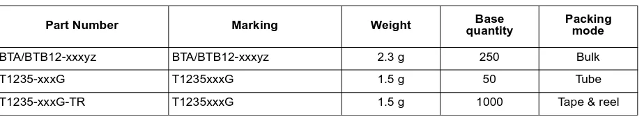
Note: xxx = voltage, yy = sensitivity, z = type
Part Number Marking Weight quantityBase Packingmode
BTA/BTB12-xxxyz BTA/BTB12-xxxyz 2.3 g 250 Bulk
T1235-xxxG T1235xxxG 1.5 g 50 Tube
T1235-xxxG-TR T1235xxxG 1.5 g 1000 Tape & reel
Fig. 1: Maximum power dissipation versus RMS
on-state current (full cycle).
Fig. 2-1: RMS on-state current versus case
temperature (full cycle).
Fig. 2-2: RMS on-state current versus ambient
temperature (printed circuit board FR4, copper thickness: 35µm),full cycle.
Fig. 3: Relative variation of thermal impedance
versus pulse duration.
0 1 2 3 4 5 6 7 8 9 10 11 12
0 2 4 6 8 10 12 14 16 P (W) IT(RMS)(A)
0 25 50 75 100 125
0 1 2 3 4 5 6 7 8 9 10 11 12 13 14 IT(RMS) (A) BTA BTB/T12 Tc(°C)
0 25 50 75 100 125
0.0 0.5 1.0 1.5 2.0 2.5 3.0 3.5 Tamb(°C) IT(RMS) (A) D PAK (S=1cm ) 2 2
1E-3 1E-2 1E-1 1E+0 1E+1 1E+2 5E+2
BTA/BTB12 and T12 Series
5/7
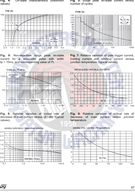
Fig. 4: On-state characteristics (maximum
values).
Fig. 5: Surge peak on-state current versus
number of cycles.
Fig. 6: Non-repetitive surge peak on-state
current for a sinusoidal pulse with width tp < 10ms, and corresponding value of I²t.
Fig. 7: Relative variation of gate trigger current,
holding current and latching current versus junction temperature (typical values).
Fig. 8: Relative variation of critical rate of
decrease of main current versus (dV/dt)c (typical values).
Fig. 9: Relative variation of critical rate of
decrease of main current versus junction temperature.
0.5 1.0 1.5 2.0 2.5 3.0 3.5 4.0 4.5 5.0
1 10 100 ITM (A) Tj=25°C Tj max Tj max. Vto = 0.85 V Rd = 35 mΩ VTM(V)
1 10 100 1000
0 10 20 30 40 50 60 70 80 90 100 110 120 130 ITSM (A) Non repetitive Tj initial=25°C Repetitive Tc=90°C One cycle t=20ms
Number of cycles
0.01 0.10 1.00 10.00
10 100 1000
ITSM (A), I²t (A²s)
Tj initial=25°C ITSM I²t dI/dt limitation: 50A/µs tp (ms)
-40 -20 0 20 40 60 80 100 120 140
0.0 0.5 1.0 1.5 2.0 2.5
IGT,IH,IL[Tj] / IGT,IH,IL [Tj=25°C]
IGT
IH & IL
Tj(°C)
0.1 1.0 10.0 100.0
0.0 0.4 0.8 1.2 1.6 2.0 2.4 2.8
(dI/dt)c [(dV/dt)c] / Specified (dI/dt)c
BW/CW/T1235 C
B SW
(dV/dt)c (V/µs)
0 25 50 75 100 125
BTA/BTB12 and T12 Series
6/7
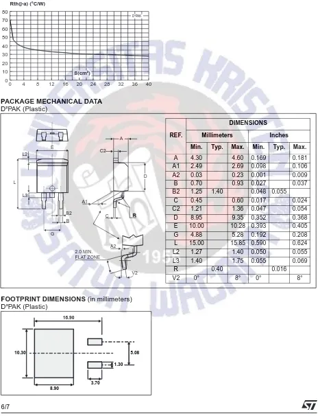
Fig. 10: D²PAK Thermal resistance junction to
ambient versus copper surface under tab (printed circuit board FR4, copper thickness: 35µm).
0 4 8 12 16 20 24 28 32 36 40
0 10 20 30 40 50 60 70 80 S(cm²) Rth(j-a) (°C/W) D²PAK
PACKAGE MECHANICAL DATA
D²PAK (Plastic)
REF.
DIMENSIONS
Millimeters Inches
Min. Typ. Max. Min. Typ. Max.
A 4.30 4.60 0.169 0.181
A1 2.49 2.69 0.098 0.106
A2 0.03 0.23 0.001 0.009
B 0.70 0.93 0.027 0.037
B2 1.25 1.40 0.048 0.055
C 0.45 0.60 0.017 0.024
C2 1.21 1.36 0.047 0.054
D 8.95 9.35 0.352 0.368
E 10.00 10.28 0.393 0.405
G 4.88 5.28 0.192 0.208
L 15.00 15.85 0.590 0.624
L2 1.27 1.40 0.050 0.055
L3 1.40 1.75 0.055 0.069
R 0.40 0.016
V2 0° 8° 0° 8°
A C2 D R 2.0 MIN. FLAT ZONE A2 V2 C A1 G L L3 L2 B B2 E
FOOTPRINT DIMENSIONS (in millimeters)
BTA/BTB12 and T12 Series
7/7
PACKAGE MECHANICAL DATA
TO-220AB / TO-220AB Ins.
REF.
DIMENSIONS
Millimeters Inches
Min. Typ. Max. Min. Typ. Max.
A 15.20 15.90 0.598 0.625
a1 3.75 0.147
a2 13.00 14.00 0.511 0.551
B 10.00 10.40 0.393 0.409
b1 0.61 0.88 0.024 0.034
b2 1.23 1.32 0.048 0.051
C 4.40 4.60 0.173 0.181
c1 0.49 0.70 0.019 0.027
c2 2.40 2.72 0.094 0.107
e 2.40 2.70 0.094 0.106
F 6.20 6.60 0.244 0.259
I 3.75 3.85 0.147 0.151
I4 15.80 16.40 16.80 0.622 0.646 0.661
L 2.65 2.95 0.104 0.116
l2 1.14 1.70 0.044 0.066
l3 1.14 1.70 0.044 0.066
M 2.60 0.102
M B
l4
C
b2
a2 l2
c2
l3
b1
a1 A
F L
I
e
c1
Information furnished is believed to be accurate and reliable. However, STMicroelectronics assumes no responsibility for the consequences of use of such information nor for any infringement of patents or other rights of third parties which may result from its use. No license is granted by implication or otherwise under any patent or patent rights of STMicroelectronics. Specifications mentioned in this publication are subject to change without notice. This publication supersedes and replaces all information previously supplied. STMicroelectronics products are not authorized for use as critical components in life support devices or systems without express written approval of STMicroelectronics.
© The ST logo is a registered trademark of STMicroelectronics
© 2000 STMicroelectronics - Printed in Italy - All Rights Reserved
STMicroelectronics GROUP OF COMPANIES
Australia - Brazil - China - Finland - France - Germany - Hong Kong - India - Italy - Japan - Malaysia - Malta - Morocco Singapore - Spain - Sweden - Switzerland - United Kingdom
TL/H/5516
LM35/LM35A/LM35C/LM35CA/LM35D
Precision
Centigrade
Temperature
Sensors
December 1994LM35/LM35A/LM35C/LM35CA/LM35D
Precision Centigrade Temperature Sensors
General Description
The LM35 series are precision integrated-circuit tempera-ture sensors, whose output voltage is linearly proportional to the Celsius (Centigrade) temperature. The LM35 thus has
an advantage over linear temperature sensors calibrated in§
Kelvin, as the user is not required to subtract a large con-stant voltage from its output to obtain convenient Centi-grade scaling. The LM35 does not require any external
cali-bration or trimming to provide typical accuracies ofg(/4§C
at room temperature andg*/4§C over a fullb55 toa150§C
temperature range. Low cost is assured by trimming and calibration at the wafer level. The LM35’s low output imped-ance, linear output, and precise inherent calibration make interfacing to readout or control circuitry especially easy. It can be used with single power supplies, or with plus and
minus supplies. As it draws only 60mA from its supply, it has
very low self-heating, less than 0.1§C in still air. The LM35 is
rated to operate over a b55§ to a150§C temperature
range, while the LM35C is rated for a b40§ to a110§C
range (b10§with improved accuracy). The LM35 series is
available packaged in hermetic TO-46 transistor packages, while the LM35C, LM35CA, and LM35D are also available in the plastic TO-92 transistor package. The LM35D is also available in an 8-lead surface mount small outline package and a plastic TO-202 package.
Features
Y Calibrated directly in§Celsius (Centigrade)
Y Lineara10.0 mV/§C scale factor
Y 0.5§C accuracy guaranteeable (ata25§C)
Y Rated for fullb55§toa150§C range
Y Suitable for remote applications
Y Low cost due to wafer-level trimming
Y Operates from 4 to 30 volts
Y Less than 60mA current drain
Y Low self-heating, 0.08§C in still air
Y Nonlinearity onlyg(/4§C typical
Y Low impedance output, 0.1Xfor 1 mA load
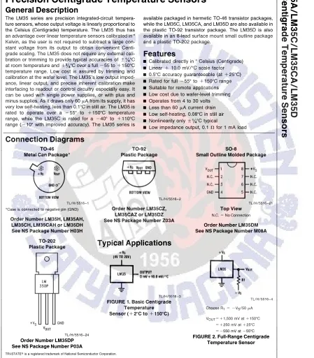
Connection Diagrams
TO-46 Metal Can Package*
TL/H/5516 – 1
*Case is connected to negative pin (GND)
Order Number LM35H, LM35AH, LM35CH, LM35CAH or LM35DH See NS Package Number H03H
TO-92 Plastic Package
TL/H/5516 – 2
Order Number LM35CZ, LM35CAZ or LM35DZ See NS Package Number Z03A
SO-8
Small Outline Molded Package
TL/H/5516 – 21
Top View N.C.eNo Connection
Order Number LM35DM See NS Package Number M08A
TO-202 Plastic Package
TL/H/5516 – 24
Order Number LM35DP See NS Package Number P03A
Typical Applications
TL/H/5516 – 3
FIGURE 1. Basic Centigrade Temperature Sensor (a2§C toa150§C)
TL/H/5516 – 4
Choose R1e bVS/50mA
VOUTe a1,500 mV ata150§C
e a250 mV ata25§C
e b550 mV atb55§C FIGURE 2. Full-Range Centigrade
Temperature Sensor
TRI-STATEÉis a registered trademark of National Semiconductor Corporation.
Absolute Maximum Ratings(Note 10)
If Military/Aerospace specified devices are required, please contact the National Semiconductor Sales Office/Distributors for availability and specifications.
Supply Voltage a35V tob0.2V
Output Voltage a6V tob1.0V
Output Current 10 mA
Storage Temp., TO-46 Package, b60§C toa180§C
TO-92 Package, b60§C toa150§C
SO-8 Package, b65§C toa150§C
TO-202 Package, b65§C toa150§C
Lead Temp.:
TO-46 Package, (Soldering, 10 seconds) 300§C
TO-92 Package, (Soldering, 10 seconds) 260§C
TO-202 Package, (Soldering, 10 seconds) a230§C
SO Package (Note 12):
Vapor Phase (60 seconds) 215§C
Infrared (15 seconds) 220§C
ESD Susceptibility (Note 11) 2500V
Specified Operating Temperature Range: TMINto TMAX
(Note 2)
LM35, LM35A b55§C toa150§C
LM35C, LM35CA b40§C toa110§C
LM35D 0§C toa100§C
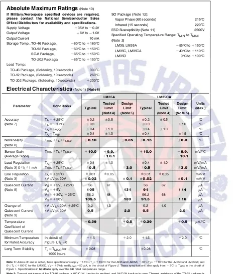
Electrical Characteristics(Note 1)(Note 6)
LM35A LM35CA
Parameter Conditions Tested Design Tested Design Units
Typical Limit Limit Typical Limit Limit (Max.)
(Note 4) (Note 5) (Note 4) (Note 5)
Accuracy TAe a25§C g0.2 g0.5 g0.2 g0.5 §C
(Note 7) TAeb10§C g0.3 g0.3 g1.0 §C
TAeTMAX g0.4 g1.0 g0.4 g1.0 §C
TAeTMIN g0.4 g1.0 g0.4 g1.5 §C
Nonlinearity TMINsTAsTMAX g0.18 g0.35 g0.15 g0.3 §C
(Note 8)
Sensor Gain TMINsTAsTMAX a10.0 a9.9, a10.0 a9.9, mV/§C
(Average Slope) a10.1 a10.1
Load Regulation TAe a25§C g0.4 g1.0 g0.4 g1.0 mV/mA
(Note 3) 0sILs1 mA TMINsTAsTMAX g0.5 g3.0 g0.5 g3.0 mV/mA
Line Regulation TAe a25§C g0.01 g0.05 g0.01 g0.05 mV/V
(Note 3) 4VsV
Ss30V g0.02 g0.1 g0.02 g0.1 mV/V
Quiescent Current VSe a5V,a25§C 56 67 56 67 mA
(Note 9) VSe a5V 105 131 91 114 mA
VSe a30V,a25§C 56.2 68 56.2 68 mA
VSe a30V 105.5 133 91.5 116 mA
Change of 4VsVSs30V,a25§C 0.2 1.0 0.2 1.0 mA
Quiescent Current 4VsVSs30V 0.5 2.0 0.5 2.0 mA
(Note 3)
Temperature a0.39 a0.5 a0.39 a0.5 mA/§C
Coefficient of Quiescent Current
Minimum Temperature In circuit of a1.5 a2.0 a1.5 a2.0 §C
for Rated Accuracy Figure 1 , ILe0
Long Term Stability TJeTMAX, for g0.08 g0.08 §C
1000 hours
Note 1:Unless otherwise noted, these specifications apply:b55§CsTJsa150§C for the LM35 and LM35A;b40§sTJsa110§C for the LM35C and LM35CA; and
0§sTJsa100§C for the LM35D. VSe a5Vdc and ILOADe50mA, in the circuit ofFigure 2. These specifications also apply froma2§C to TMAXin the circuit of Figure 1 . Specifications inboldfaceapply over the full rated temperature range.
Note 2:Thermal resistance of the TO-46 package is 400§C/W, junction to ambient, and 24§C/W junction to case. Thermal resistance of the TO-92 package is 180§C/W junction to ambient. Thermal resistance of the small outline molded package is 220§C/W junction to ambient. Thermal resistance of the TO-202 package is 85§C/W junction to ambient. For additional thermal resistance information see table in the Applications section.
Electrical Characteristics(Note 1)(Note 6)(Continued)
LM35 LM35C, LM35D
Parameter Conditions Tested Design Tested Design Units
Typical Limit Limit Typical Limit Limit (Max.)
(Note 4) (Note 5) (Note 4) (Note 5)
Accuracy, TAe a25§C g0.4 g1.0 g0.4 g1.0 §C
LM35, LM35C TAeb10§C g0.5 g0.5 g1.5 §C
(Note 7) TAeTMAX g0.8 g1.5 g0.8 g1.5 §C
TAeTMIN g0.8 g1.5 g0.8 g2.0 §C
Accuracy, TAe a25§C g0.6 g1.5 §C
LM35D TAeTMAX g0.9 g2.0 §C
(Note 7) TAeTMIN g0.9 g2.0 §C
Nonlinearity TMINsTAsTMAX g0.3 g0.5 g0.2 g0.5 §C
(Note 8)
Sensor Gain TMINsTAsTMAX a10.0 a9.8, a10.0 a9.8, mV/§C
(Average Slope) a10.2 a10.2
Load Regulation TAe a25§C g0.4 g2.0 g0.4 g2.0 mV/mA
(Note 3) 0sILs1 mA TMINsTAsTMAX g0.5 g5.0 g0.5 g5.0 mV/mA
Line Regulation TAe a25§C g0.01 g0.1 g0.01 g0.1 mV/V
(Note 3) 4VsVSs30V g0.02 g0.2 g0.02 g0.2 mV/V
Quiescent Current VSe a5V,a25§C 56 80 56 80 mA
(Note 9) VSe a5V 105 158 91 138 mA
VSe a30V,a25§C 56.2 82 56.2 82 mA
VSe a30V 105.5 161 91.5 141 mA
Change of 4VsVSs30V,a25§C 0.2 2.0 0.2 2.0 mA
Quiescent Current 4VsV
Ss30V 0.5 3.0 0.5 3.0 mA
(Note 3)
Temperature a0.39 a0.7 a0.39 a0.7 mA/§C
Coefficient of Quiescent Current
Minimum Temperature In circuit of a1.5 a2.0 a1.5 a2.0 §C
for Rated Accuracy Figure 1 , ILe0
Long Term Stability TJeTMAX, for g0.08 g0.08 §C
1000 hours
Note 3:Regulation is measured at constant junction temperature, using pulse testing with a low duty cycle. Changes in output due to heating effects can be computed by multiplying the internal dissipation by the thermal resistance.
Note 4:Tested Limits are guaranteed and 100% tested in production.
Note 5:Design Limits are guaranteed (but not 100% production tested) over the indicated temperature and supply voltage ranges. These limits are not used to calculate outgoing quality levels.
Note 6:Specifications inboldfaceapply over the full rated temperature range.
Note 7:Accuracy is defined as the error between the output voltage and 10mv/§C times the device’s case temperature, at specified conditions of voltage, current, and temperature (expressed in§C).
Note 8:Nonlinearity is defined as the deviation of the output-voltage-versus-temperature curve from the best-fit straight line, over the device’s rated temperature range.
Note 9:Quiescent current is defined in the circuit ofFigure 1 .
Note 10:Absolute Maximum Ratings indicate limits beyond which damage to the device may occur. DC and AC electrical specifications do not apply when operating the device beyond its rated operating conditions. See Note 1.
Note 11:Human body model, 100 pF discharged through a 1.5 kXresistor.
Note 12:See AN-450 ‘‘Surface Mounting Methods and Their Effect on Product Reliability’’ or the section titled ‘‘Surface Mount’’ found in a current National Semiconductor Linear Data Book for other methods of soldering surface mount devices.
[image:30.612.81.533.93.670.2]Typical Performance Characteristics
Thermal Resistance
Junction to Air Thermal Time Constant
Thermal Response in Still Air
Thermal Response in Stirred Oil Bath
Minimum Supply Voltage vs. Temperature
Quiescent Current vs. Temperature (In Circuit ofFigure 1 .)
TL/H/5516 – 17
Quiescent Current vs. Temperature (In Circuit ofFigure 2 .)
Accuracy vs. Temperature (Guaranteed)
Accuracy vs. Temperature (Guaranteed)
TL/H/5516 – 18
Start-Up Response Noise Voltage
TL/H/5516 – 22
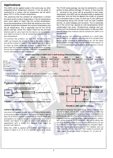
Applications
The LM35 can be applied easily in the same way as other integrated-circuit temperature sensors. It can be glued or cemented to a surface and its temperature will be within
about 0.01§C of the surface temperature.
This presumes that the ambient air temperature is almost the same as the surface temperature; if the air temperature were much higher or lower than the surface temperature, the actual temperature of the LM35 die would be at an inter-mediate temperature between the surface temperature and the air temperature. This is expecially true for the TO-92 plastic package, where the copper leads are the principal thermal path to carry heat into the device, so its tempera-ture might be closer to the air temperatempera-ture than to the sur-face temperature.
To minimize this problem, be sure that the wiring to the LM35, as it leaves the device, is held at the same tempera-ture as the surface of interest. The easiest way to do this is to cover up these wires with a bead of epoxy which will insure that the leads and wires are all at the same tempera-ture as the surface, and that the LM35 die’s temperatempera-ture will not be affected by the air temperature.
The TO-46 metal package can also be soldered to a metal surface or pipe without damage. Of course, in that case the
Vbterminal of the circuit will be grounded to that metal.
Alternatively, the LM35 can be mounted inside a sealed-end metal tube, and can then be dipped into a bath or screwed into a threaded hole in a tank. As with any IC, the LM35 and accompanying wiring and circuits must be kept insulated and dry, to avoid leakage and corrosion. This is especially true if the circuit may operate at cold temperatures where condensation can occur. Printed-circuit coatings and var-nishes such as Humiseal and epoxy paints or dips are often used to insure that moisture cannot corrode the LM35 or its connections.
These devices are sometimes soldered to a small light-weight heat fin, to decrease the thermal time constant and speed up the response in slowly-moving air. On the other hand, a small thermal mass may be added to the sensor, to give the steadiest reading despite small deviations in the air temperature.
Temperature Rise of LM35 Due To Self-heating (Thermal Resistance)
TO-46, TO-46, TO-92, TO-92, SO-8 SO-8 TO-202 TO-202*** no heat sink small heat fin* no heat sink small heat fin** no heat sink small heat fin** no heat sink small heat fin Still air 400§C/W 100§C/W 180§C/W 140§C/W 220§C/W 110§C/W 85§C/W 60§C/W Moving air 100§C/W 40§C/W 90§C/W 70§C/W 105§C/W 90§C/W 25§C/W 40§C/W Still oil 100§C/W 40§C/W 90§C/W 70§C/W
Stirred oil 50§C/W 30§C/W 45§C/W 40§C/W (Clamped to metal,
Infinite heat sink) (24§C/W) (55§C/W) (23§C/W)
*Wakefield type 201, or 1×disc of 0.020×sheet brass, soldered to case, or similar.
**TO-92 and SO-8 packages glued and leads soldered to 1×square of(/16×printed circuit board with 2 oz. foil or similar.
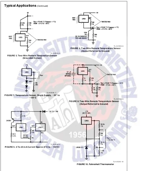
Typical Applications(Continued)
TL/H/5516 – 19
FIGURE 3. LM35 with Decoupling from Capacitive Load
TL/H/5516 – 20
FIGURE 4. LM35 with R-C Damper
CAPACITIVE LOADS
Like most micropower circuits, the LM35 has a limited ability to drive heavy capacitive loads. The LM35 by itself is able to drive 50 pf without special precautions. If heavier loads are anticipated, it is easy to isolate or decouple the load with a
resistor; seeFigure 3 . Or you can improve the tolerance of
capacitance with a series R-C damper from output to
ground; seeFigure 4 .
When the LM35 is applied with a 200X load resistor as
shown inFigure 5, 6, or 8, it is relatively immune to wiring
capacitance because the capacitance forms a bypass from ground to input, not on the output. However, as with any linear circuit connected to wires in a hostile environment, its performance can be affected adversely by intense electro-magnetic sources such as relays, radio transmitters, motors with arcing brushes, SCR transients, etc, as its wiring can act as a receiving antenna and its internal junctions can act as rectifiers. For best results in such cases, a bypass
capac-itor from VINto ground and a series R-C damper such as
75Xin series with 0.2 or 1mF from output to ground are
often useful. These are shown inFigures 13, 14, and 16.
[image:32.612.83.532.66.692.2]Typical Applications(Continued)
TL/H/5516 – 5
FIGURE 5. Two-Wire Remote Temperature Sensor (Grounded Sensor)
TL/H/5516 – 6
FIGURE 6. Two-Wire Remote Temperature Sensor (Output Referred to Ground)
TL/H/5516 – 7
FIGURE 7. Temperature Sensor, Single Supply,b55§to
a150§C
TL/H/5516 – 8
FIGURE 8. Two-Wire Remote Temperature Sensor (Output Referred to Ground)
TL/H/5516 – 9
FIGURE 9. 4-To-20 mA Current Source (0§C toa100§C)
TL/H/5516 – 10
FIGURE 10. Fahrenheit Thermometer
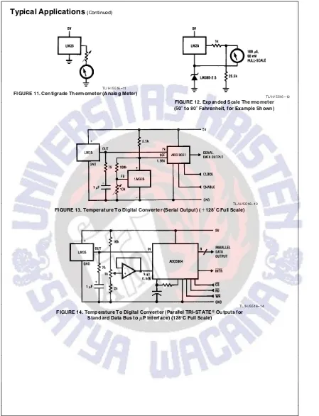
[image:33.612.57.533.67.632.2]Typical Applications(Continued)
TL/H/5516 – 11
FIGURE 11. Centigrade Thermometer (Analog Meter)
TL/H/5516 – 12
FIGURE 12. Expanded Scale Thermometer
(50§to 80§Fahrenheit, for Example Shown)
TL/H/5516 – 13
FIGURE 13. Temperature To Digital Converter (Serial Output) (a128§C Full Scale)
TL/H/5516 – 14
FIGURE 14. Temperature To Digital Converter (Parallel TRI-STATEÉOutputs for
Standard Data Bus tomP Interface) (128§C Full Scale)
[image:34.612.85.534.69.655.2]Typical Applications(Continued)
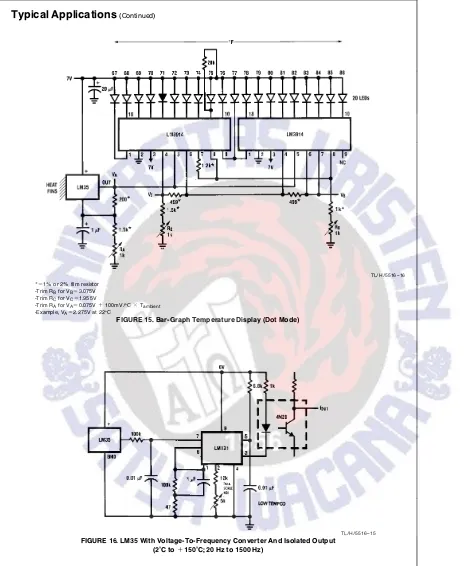
TL/H/5516 – 16
*e1% or 2% film resistor -Trim RBfor VBe3.075V
-Trim RCfor VCe1.955V
-Trim RAfor VAe0.075Va100mV/§CcTambient
-Example, VAe2.275V at 22§C
FIGURE 15. Bar-Graph Temperature Display (Dot Mode)
TL/H/5516 – 15
FIGURE 16. LM35 With Voltage-To-Frequency Converter And Isolated Output (2§C toa150§C; 20 Hz to 1500 Hz)
[image:35.612.60.535.71.637.2]Block Diagram
TL/H/5516 – 23
Physical Dimensionsinches (millimeters)
TO-46 Metal Can Package (H) Order Number LM35H, LM35AH, LM35CH,
LM35CAH, or LM35DH NS Package Number H03H
SO-8 Molded Small Outline Package (M) Order Number LM35DM NS Package Number M08A
Physical Dimensionsinches (millimeters) (Continued)
Power Package TO-202 (P) Order Number LM35DP NS Package Number P03A
LM35/LM35A/LM35C/LM35CA/LM35D
Precision
Centigrade
Temperature
Sensors
Physical Dimensionsinches (millimeters) (Continued)
TO-92 Plastic Package (Z) Order Number LM35CZ, LM35CAZ or LM35DZ
NS Package Number Z03A
LIFE SUPPORT POLICY
NATIONAL’S PRODUCTS ARE NOT AUTHORIZED FOR USE AS CRITICAL COMPONENTS IN LIFE SUPPORT DEVICES OR SYSTEMS WITHOUT THE EXPRESS WRITTEN APPROVAL OF THE PRESIDENT OF NATIONAL SEMICONDUCTOR CORPORATION. As used herein:
1. Life support devices or systems are devices or 2. A critical component is any component of a life
systems which, (a) are intended for surgical implant support device or system whose failure to perform can
into the body, or (b) support or sustain life, and whose be reasonably expected to cause the failure of the life
failure to perform, when properly used in accordance support device or system, or to affect its safety or
with instructions for use provided in the labeling, can effectiveness.
be reasonably expected to result in a significant injury to the user.
National Semiconductor National Semiconductor National Semiconductor National Semiconductor National Semiconductores National Semiconductor Corporation GmbH Japan Ltd. Hong Kong Ltd. Do Brazil Ltda. (Australia) Pty, Ltd.
2900 Semiconductor Drive Livry-Gargan-Str. 10 Sumitomo Chemical 13th Floor, Straight Block, Rue Deputado Lacorda Franco Building 16 P.O. Box 58090 D-82256 F4urstenfeldbruck Engineering Center Ocean Centre, 5 Canton Rd. 120-3A Business Park Drive
Santa Clara, CA 95052-8090 Germany Bldg. 7F Tsimshatsui, Kowloon Sao Paulo-SP Monash Business Park
Tel: 1(800) 272-9959 Tel: (81-41) 35-0 1-7-1, Nakase, Mihama-Ku Hong Kong Brazil 05418-000 Nottinghill, Melbourne TWX: (910) 339-9240 Telex: 527649 Chiba-City, Tel: (852) 2737-1600 Tel: (55-11) 212-5066 Victoria 3168 Australia
Fax: (81-41) 35-1 Ciba Prefecture 261 Fax: (852) 2736-9960 Telex: 391-1131931 NSBR BR Tel: (3) 558-9999
Tel: (043) 299-2300 Fax: (55-11) 212-1181 Fax: (3) 558-9998
Fax: (043) 299-2500
µ
A7800 SERIES
POSITIVE-VOLTAGE REGULATORS
SLVS056J – MAY 1976 – REVISED MAY 2003
1
POST OFFICE BOX 655303 • DALLAS, TEXAS 75265
D
3-Terminal RegulatorsD
Output Current up to 1.5 AD
Internal Thermal-Overload ProtectionD
High Power-Dissipation CapabilityD
Internal Short-Circuit Current LimitingD
Output Transistor Safe-Area CompensationKTE PACKAGE (TOP VIEW) OUTPUT COMMON INPUT COMMON OUTPUT
KC (TO-220) PACKAGE (TOP VIEW)
INPUT
COMMON
COMMON OUTPUT
KCS (TO-220) PACKAGE (TOP VIEW)
INPUT
COMMON
COMMON
description/ordering information
This series of fixed-voltage integrated-circuit voltage regulators is designed for a wide range of applications. These applications include on-card regulation for elimination of noise and distribution problems associated with single-point regulation. Each of these regulators can deliver up to 1.5 A of output current. The internal current-limiting and thermal-shutdown features of these regulators essentially make them immune to overload. In addition to use as fixed-voltage regulators, these devices can be used with external components to obtain adjustable output voltages and currents, and also can be used as the power-pass element in precision regulators.
ORDERING INFORMATION
TJ VO(NOM)(V) PACKAGE† ORDERABLE
PART NUMBER
TOP-SIDE MARKING
POWER-FLEX (KTE) Reel of 2000 µA7805CKTER µA7805C
5 TO-220 (KC) Tube of 50 µA7805CKC
µA7805C
TO-220, short shoulder (KCS) Tube of 20 µA7805CKCS µA7805C
POWER-FLEX (KTE) Reel of 2000 µA7808CKTER µA7808C
8 TO-220 (KC) Tube of 50 µA7808CKC
µA7808C
TO-220, short shoulder (KCS) Tube of 20 µA7808CKCS µA7808C
10 POWER-FLEX (KTE) Reel of 2000 µA7810CKTER µA7810C
0°C to 125°C
10
TO-220 (KC) Tube of 50 µA7810CKC µA7810C
0°C to 125°C
POWER-FLEX (KTE) Reel of 2000 µA7812CKTER µA7812C
12 TO-220 (KC) Tube of 50 µA7812CKC
µA7812C
TO-220, short shoulder (KCS) Tube of 20 µA7812CKCS µA7812C
POWER-FLEX (KTE) Reel of 2000 µA7815CKTER µA7815C
15 TO-220 (KC) Tube of 50 µA7815CKC
µA7815C
TO-220, short shoulder (KCS) Tube of 20 µA7815CKCS µA7815C
24 POWER-FLEX (KTE) Reel of 2000 µA7824CKTER µA7824C
24
TO-220 (KC) Tube of 50 µA7824CKC µA7824C
† Package drawings, standard packing quantities, thermal data, symbolization, and PCB design guidelines are available at www.ti.com/sc/package.
Please be aware that an important notice concerning availability, standard warranty, and use in critical applications of Texas Instruments semiconductor products and disclaimers thereto appears at the end of this data sheet.
Copyright 2003, Texas Instruments Incorporated
µ
A7800 SERIES
POSITIVE-VOLTAGE REGULATORS
SLVS056J – MAY 1976 – REVISED MAY 2003
2 POST OFFICE BOX 655303 • DALLAS, TEXAS 75265
schematic
INPUT
OUTPUT
COMMON
absolute maximum ratings over virtual junction temperature range (unless otherwise noted)†
Input voltage, VI: µA7824C . . . 40 V All others . . . 35 V Operating virtual junction temperature, TJ 150. . . °C Lead temperature 1,6 mm (1/16 inch) from case for 10 seconds . . . 260°C Storage temperature range, Tstg. . . –65°C to 150°C
† Stresses beyond those listed under “absolute maximum ratings” may cause permanent damage to the device. These are stress ratings only, and functional operation of the device at these or any other conditions beyond those indicated under “recommended operating conditions” is not implied. Exposure to absolute-maximum-rated conditions for extended periods may affect device reliability.
package thermal data (see Note 1)
PACKAGE BOARD θJC θJA
POWER-FLEX (KTE) High K, JESD 51-5 3°C/W 23°C/W
TO-220 (KC/KCS) High K, JESD 51-5 3°C/W 19°C/W
µ
A7800 SERIES
POSITIVE-VOLTAGE REGULATORS
SLVS056J – MAY 1976 – REVISED MAY 2003
3
POST OFFICE BOX 655303 • DALLAS, TEXAS 75265
recommended operating conditions
MIN MAX UNIT
µA7805C 7 25
µA7808C 10.5 25
VI Input voltage µA7810C 12.5 28 V
VI Input voltage
µA7812C 14.5 30 V
µA7815C 17.5 30
µA7824C 27 38
IO Output current 1.5 A
TJ Operating virtual junction temperature µA7800C series 0 125 °C
electrical characteristics at specified virtual junction temperature, VI = 10 V, IO = 500 mA (unless otherwise noted)
PARAMETER TEST CONDITIONS T † µA7805C UNIT
PARAMETER TEST CONDITIONS TJ†
MIN TYP MAX UNIT
Output voltage IO = 5 mA to 1 A, VI = 7 V to 20 V, 25°C 4.8 5 5.2 V
Output voltage O ,
PD ≤ 15 W
I ,
0°C to 125°C 4.75 5.25 V
Input voltage regulation VI = 7 V to 25 V 25°C 3 100 mV
Input voltage regulation
VI = 8 V to 12 V 25°C 1 50 mV
Ripple rejection VI = 8 V to 18 V, f = 120 Hz 0°C to 125°C 62 78 dB
Output voltage regulation IO = 5 mA to 1.5 A 25°C 15 100 mV
Output voltage regulation
IO = 250 mA to 750 mA 25°C 5 50 mV
Output resistance f = 1 kHz 0°C to 125°C 0.017 Ω
Temperature coefficient of output voltage IO = 5 mA 0°C to 125°C –1.1 mV/°C
Output noise voltage f = 10 Hz to 100 kHz 25°C 40 µV
Dropout voltage IO = 1 A 25°C 2 V
Bias current 25°C 4.2 8 mA
Bias current change VI = 7 V to 25 V 0°C t 125°C
1.3 mA Bias current change
IO = 5 mA to 1 A 0°C to 125°C 0.5 mA
Short-circuit output current 25°C 750 mA
Peak output current 25°C 2.2 A
µ
A7800 SERIES
POSITIVE-VOLTAGE REGULATORS
SLVS056J – MAY 1976 – REVISED MAY 2003
4 POST OFFICE BOX 655303 • DALLAS, TEXAS 75265
electrical characteristics at specified virtual junction temperature, VI = 14 V, IO = 500 mA (unless otherwise noted)
PARAMETER TEST CONDITIONS T † µ
A7808C
UNIT
PARAMETER TEST CONDITIONS TJ†
MIN TYP MAX UNIT
Output voltage IO = 5 mA to 1 A, VI = 10.5 V to 23 V, 25°C 7.7 8 8.3 V
Output voltage O ,
PD ≤ 15 W
I ,
0°C to 125°C 7.6 8.4 V
Input voltage regulation VI = 10.5 V to 25 V 25°C 6 160 mV
Input voltage regulation
VI = 11 V to 17 V 25°C 2 80 mV
Ripple rejection VI = 11.5 V to 21.5 V, f = 120 Hz 0°C to 125°C 55 72 dB
Output voltage regulation IO = 5 mA to 1.5 A 25°C 12 160 mV
Output voltage regulation
IO = 250 mA to 750 mA 25°C 4 80 mV
Output resistance f = 1 kHz 0°C to 125°C 0.016 Ω
Temperature coefficient of output voltage IO = 5 mA 0°C to 125°C –0.8 mV/°C
Output noise voltage f = 10 Hz to 100 kHz 25°C 52 µV
Dropout voltage IO = 1 A 25°C 2 V
Bias current 25°C 4.3 8 mA
Bias current change VI = 10.5 V to 25 V 0°C to 125°C 1 mA
Bias current change
IO = 5 mA to 1 A 0°C to 125°C 0.5 mA
Short-circuit output current 25°C 450 mA
Peak output current 25°C 2.2 A
† Pulse-testing techniques maintain the junction temperature as close to the ambient temperature as possible. Thermal effects must be taken into account separately. All characteristics are measured with a 0.33-µF capacitor across the input and a 0.1-µF capacitor across the output.
electrical characteristics at specified virtual junction temperature, VI = 17 V, IO = 500 mA (unless otherwise noted)
PARAMETER TEST CONDITIONS T † µ
A7810C
UNIT
PARAMETER TEST CONDITIONS TJ†
MIN TYP MAX UNIT
Output voltage IO = 5 mA to 1 A, VI = 12.5 V to 25 V, 25°C 9.6 10 10.4 V
Output voltage O ,
PD ≤ 15 W
I ,
0°C to 125°C 9.5 10 10.5 V
Input voltage regulation VI = 12.5 V to 28 V 25°C 7 200 mV
Input voltage regulation
VI = 14 V to 20 V 25°C 2 100 mV
Ripple rejection VI = 13 V to 23 V, f = 120 Hz 0°C to 125°C 55 71 dB
Output voltage regulation IO = 5 mA to 1.5 A 25°C 12 200 mV
Output voltage regulation
IO = 250 mA to 750 mA 25°C 4 100 mV
Output resistance f = 1 kHz 0°C to 125°C 0.018 Ω
Temperature coefficient of output voltage IO = 5 mA 0°C to 125°C –1 mV/°C
Output noise voltage f = 10 Hz to 100 kHz 25°C 70 µV
Dropout voltage IO = 1 A 25°C 2 V
Bias current 25°C 4.3 8 mA
Bias current change VI = 12.5 V to 28 V 0°C to 125°C 1 mA
Bias current change
IO = 5 mA to 1 A 0°C to 125°C 0.5 mA
Short-circuit output current 25°C 400 mA
Peak output current 25°C 2.2 A
µ
A7800 SERIES
POSITIVE-VOLTAGE REGULATORS
SLVS056J – MAY 1976 – REVISED MAY 2003
5
POST OFFICE BOX 655303 • DALLAS, TEXAS 75265
electrical characteristics at specified virtual junction temperature, VI = 19 V, IO = 500 mA (unless otherwise noted)
PARAMETER TEST CONDITIONS T † µ
A7812C
UNIT
PARAMETER TEST CONDITIONS TJ†
MIN TYP MAX UNIT
Output voltage IO = 5 mA to 1 A, VI = 14.5 V to 27 V, 25°C 11.5 12 12.5 V
Output voltage O ,
PD ≤ 15 W
I ,
0°C to 125°C 11.4 12.6 V
Input voltage regulation VI = 14.5 V to 30 V 25°C 10 240 mV
Input voltage regulation
VI = 16 V to 22 V 25°C 3 120 mV
Ripple rejection VI = 15 V to 25 V, f = 120 Hz 0°C to 125°C 55 71 dB
Output voltage regulation IO = 5 mA to 1.5 A 25°C 12 240 mV
Output voltage regulation
IO = 250 mA to 750 mA 25°C 4 120 mV
Output resistance f = 1 kHz 0°C to 125°C 0.018 Ω
Temperature coefficient of output voltage IO = 5 mA 0°C to 125°C –1 mV/°C
Output noise voltage f = 10 Hz to 100 kHz 25°C 75 µV
Dropout voltage IO = 1 A 25°C 2 V
Bias current 25°C 4.3 8 mA
Bias current change VI = 14.5 V to 30 V 0°C t 125°C
1 mA Bias current change
IO = 5 mA to 1 A 0°C to 125°C 0.5 mA
Short-circuit output current 25°C 350 mA
Peak output current 25°C 2.2 A
† Pulse-testing techniques maintain the junction temperature as close to the ambient temperature as possible. Thermal effects must be taken into account separately. All characteristics are measured with a 0.33-µF capacitor across the input and a 0.1-µF capacitor across the output.
electrical characteristics at specified virtual junction temperature, VI = 23 V, IO = 500 mA (unless otherwise noted)
PARAMETER TEST CONDITIONS T † µ
A7815C
UNIT
PARAMETER TEST CONDITIONS TJ†
MIN TYP MAX UNIT
Output voltage IO = 5 mA to 1 A, VI = 17.5 V to 30 V, 25°C 14.4 15 15.6 V
Output voltage O ,
PD ≤ 15 W
I ,
0°C to 125°C 14.25 15.75 V
Input voltage regulation VI = 17.5 V to 30 V 25°C 11 300 mV
Input voltage regulation
VI = 20 V to 26 V 25°C 3 150 mV
Ripple rejection VI = 18.5 V to 28.5 V, f = 120 Hz 0°C to 125°C 54 70 dB
Output voltage regulation IO = 5 mA to 1.5 A 25°C 12 300 mV
Output voltage regulation
IO = 250 mA to 750 mA 25°C 4 150 mV
Output resistance f = 1 kHz 0°C to 125°C 0.019 Ω
Temperature coefficient of output voltage IO = 5 mA 0°C to 125°C –1 mV/°C
Output noise voltage f = 10 Hz to 100 kHz 25°C 90 µV
Dropout voltage IO = 1 A 25°C 2 V
Bias current 25°C 4.4 8 mA
Bias current change VI = 17.5 V to 30 V 0°C to 125°C 1 mA
Bias current change
IO = 5 mA to 1 A 0°C to 125°C 0.5 mA
Short-circuit output current 25°C 230 mA
Peak output current 25°C 2.1 A
µ
A7800 SERIES
POSITIVE-VOLTAGE REGULATORS
SLVS056J – MAY 1976 – REVISED MAY 2003
6 POST OFFICE BOX 655303 • DALLAS, TEXAS 75265
electrical characteristics at specified virtual junction temperature, VI = 33 V, IO = 500 mA (unless otherwise noted)
PARAMETER TEST CONDITIONS T † µ
A7824C
UNIT
PARAMETER TEST CONDITIONS TJ†
MIN TYP MAX UNIT
Output voltage IO = 5 mA to 1 A, VI = 27 V to 38 V, 25°C 23 24 25 V
Output voltage O ,
PD ≤ 15 W
I ,
0°C to 125°C 22.8 25.2 V
Input voltage regulation VI = 27 V to 38 V 25°C 18 480 mV
Input voltage regulation
VI = 30 V to 36 V 25°C 6 240 mV
Ripple rejection VI = 28 V to 38 V, f = 120 Hz 0°C to 125°C 50 66 dB
Output voltage regulation IO = 5 mA to 1.5 A 25°C 12 480 mV
Output voltage regulation
IO = 250 mA to 750 mA 25°C 4 240 mV
Output resistance f = 1 kHz 0°C to 125°C 0.028 Ω
Temperature coefficient of output voltage IO = 5 mA 0°C to 125°C –1.5 mV/°C
Output noise voltage f = 10 Hz to 100 kHz 25°C 170 µV
Dropout voltage IO = 1 A 25°C 2 V
Bias current 25°C 4.6 8 mA
Bias current change VI = 27 V to 38 V 0°C to 125°C 1 mA
Bias current change
IO = 5 mA to 1 A 0°C to 125°C 0.5 mA
Short-circuit output current 25°C 150 mA
Peak output current 25°C 2.1 A
µ
A7800 SERIES
POSITIVE-VOLTAGE REGULATORS
SLVS056J – MAY 1976 – REVISED MAY 2003
7
POST OFFICE BOX 655303 • DALLAS, TEXAS 75265
APPLICATION INFORMATION
+VO +V
0.1 µF 0.33 µF
µA78xx
Figure 1. Fixed-Output Regulator
OUT IN
G
–VO COM
+
–
VI IL
µA78xx
Figure 2. Positive Regulator in Negative Configuration (VI Must Float)
R1
0.33 µF
Input µA78xx Output
0.1 µF IO
R2
VO+Vxx)
ǒ
Vxx
R1)IQ
Ǔ
R2NOTE A: The following formula is used when Vxx is the nominal output voltage (output to common) of the fixed regulator:
Figure 3. Adjustable-Output Regulator
VO(Reg) R1 Input
IO IO = (VO/R1) + IO Bias Current
0.33 µF µA78xx
[image:46.612.73.527.71.640.2]Output
µ
A7800 SERIES
POSITIVE-VOLTAGE REGULATORS
SLVS056J – MAY 1976 – REVISED MAY 2003
8 POST OFFICE BOX 655303 • DALLAS, TEXAS 75265
APPLICATION INFORMATION
µA7815C
0.1 µF 1N4001
0.1 µF
1N4001 0.33 µF
2 µF
1N4001 1N4001
VO = 15 V
VO = –15 V 20-V Input
–20-V Input µA7915C
[image:47.612.126.500.81.317.2]1 µF
Figure 5. Regulated Dual Supply
operation with a load common to a voltage of opposite polarity
In many cases, a regulator powers a load that is not connected to ground but, instead, is connected to a voltage source of opposite polarity (e.g., operational amplifiers, level-shifting circuits, etc.). In these cases, a clamp diode should be connected to the regulator output as shown in Figure 6. This protects the regulator from output polarity reversals during startup and short-circuit operation.
µA78xx +VO
+VI
–VO 1N4001
[image:47.612.91.519.368.510.2]or Equivalent
Figure 6. Output Polarity-Reversal-Protection Circuit
reverse-bias protection
Occasionally, the input voltage to the regulator can collapse faster than the output voltage. This can occur, for example, when the input supply is crowbarred during an output overvoltage condition. If the output voltage is greater than approximately 7 V, the emitter-base junction of the series-pass element (internal or external) could break down and be damaged. To prevent this, a diode shunt can be used as shown in Figure 7.
µA78xx +VO
VI
[image:47.612.205.382.561.646.2]MECHANICAL DATA
MPFM001E – OCTOBER 1994 – REVISED JANUARY 2001
1
POST OFFICE BOX 655303 • DALLAS, TEXAS 75265
KTE (R-PSFM-G3) PowerFLEX PLASTIC FLANGE-MOUNT
0.360 (9,14) 0.350 (8,89)
0.080 (2,03) 0.070 (1,78)
0.010 (0,25) NOM 0.040 (1,02)
Seating Plane 0.050 (1,27)
0.001 (0,03) 0.005 (0,13)
0.010 (0,25) NOM
Gage Plane
0.010 (0,25)
0.031 (0,79) 0.041 (1,04)
4073375/F 12/00 NOM
3 1
0.350 (8,89)
0.220 (5,59) 0.360 (9,14)
0.295 (7,49) NOM
0.320 (8,13) 0.310 (7,87)
0.025 (0,63) 0.031 (0,79)
Thermal Tab (See Note C)
0.004 (0,10)
M
0.010 (0,25) 0.100 (2,54)
3°– 6° 0.410 (10,41)
0.420 (10,67)
0.200 (5,08)
0.365 (9,27) 0.375 (9,52)
NOTES: A. All linear dimensions are in inches (millimeters). B. This drawing is subject to change without notice.
C. The center lead is in electrical contact with the thermal tab.
D. Dimensions do not include mold protrusions, not to exceed 0.006 (0,15). E. Falls within JEDEC MO-169
IMPORTANT NOTICE
Texas Instruments Incorporated and its subsidiaries (TI) reserve the right to make corrections, modifications, enhancements, improvements, and other changes to its products and services at any time and to discontinue any product or service without notice. Customers should obtain the latest relevant information before placing orders and should verify that such information is current and complete. All products are sold subject to TI’s terms and conditions of sale supplied at the time of order acknowledgment.
TI warrants performance of its hardware products to the specifications applicable at the time of sale in accordance with TI’s standard warranty. Testing and other quality control techniques are used to the extent TI deems necessary to support this warranty. Except where mandated by government requirements, testing of all parameters of each product is not necessarily performed.
TI assumes no liability for applications assistance or customer product design. Customers are responsible for their products and applications using TI components. To minimize the risks associated with customer products and applications, customers should provide adequate design and operating safeguards.
TI does not warrant or represent that any license, either express or implied, is granted under any TI patent right, copyright, mask work right, or other TI intellectual property right relating to any combination, machine, or process in which TI products or services are used. Information published by TI regarding third-party products or services does not constitute a license from TI to use such products or services or a warranty or endorsement thereof. Use of such information may require a license from a third party under the patents or other intellectual property of the third party, or a license from TI under the patents or other intellectual property of TI.
Reproduction of information in TI data books or data sheets is permissible only if reproduction is without alteration and is accompanied by all associated warranties, conditions, limitations, and notices. Reproduction of this information with alteration is an unfair and deceptive business practice. TI is not responsible or liable for such altered documentation.
Resale of TI products or services with statements different from or beyond the parameters stated by TI for that product or service voids all express and any implied warranties for the associated TI product or service and is an unfair and deceptive business practice. TI is not responsible or liable for any such statements.
Following are URLs where you can obtain information on other Texas Instruments products and application solutions:
Products Applications
Amplifiers amplifier.ti.com Audio www.ti.com/audio
Data Converters dataconverter.ti.com Automotive www.ti.com/automotive
DSP dsp.ti.com Broadband www.ti.com/broadband
Interface interface.ti.com Digital Control www.ti.com/digitalcontrol
Logic logic.ti.com Military www.ti.com/military
Power Mgmt power.ti.com Optical Networking www.ti.com/opticalnetwork
Microcontrollers microcontroller.ti.com Security www.ti.com/security
Telephony www.ti.com/telephony
Video & Imaging www.ti.com/video
Wireless www.ti.com/wireless
Mailing Address: Texas Instruments
Post Office Box 655303 Dallas, Texas 75265