Electrical characterization of P3 isolation lines patterned with a UV laser
incident from the film side on thin-film silicon solar cells
S. Ku
a,b, B.E. Pieters
b,n, S. Haas
b, A. Bauer
b, Q. Ye
a, U. Rau
b aDepartment of Physics, Shanghai Jiao Tong University, 200240 Shanghai, China
bIEK5-Photovoltaik, Forschungszentrum J¨ulich, Germany
a r t i c l e
i n f o
Article history:
Received 13 June 2012 Received in revised form 7 September 2012
Accepted 17 September 2012 Available online 11 October 2012
Keywords:
Laser scribing
a-Si:H=mc-Si:H solar modules Direct ablation
a b s t r a c t
We investigate the properties of P3 isolation lines ina-Si:H=mc-Si:H solar modules, prepared with a
nano-second pulsed UV laser incident from the film side of the solar module. For the electrical characterization of the P3 lines we developed a method which allows us to distinguish between leakage currents directly across the P3 line, leakage currents along the laser line side walls and to monitor changes in conductivity of the TCO underneath the line. We applied the developed characterization method to a series of P3 lines where we systematically varied the used laser parameters. In addition we analyzed selected P3 lines using Scanning Electron Microscopy. From the systematic variation we find that a high leakage current directly across the P3 lines is observed when the back contact is not fully removed. The best P3 lines have the back contact fully removed but an incomplete removal of the silicon in the line. When the silicon layer stack is fully removed in the P3 line we observe an increase in leakage current along the side walls of the laser lines. The best P3 laser line we obtained exhibits a very low leakage current density of only 1:5mA cm1at 1 V.
&2012 Elsevier B.V. All rights reserved.
1. Introduction
One of the advantages of thin-film solar cells is the possibility to monolithically interconnect the module during the deposition process. To this end, deposition processes and scribing processes are applied alternately. In the commonly used laser scribing methods for thin film silicon solar modules the laser beam is incident through the (transparent) superstrate to remove the film. However, there are emerging flexible thin-film technologies where the solar cells are deposited on substrates such as plastics
and metal foils[1–4]. For modules with opaque substrates the
active layer and back contact layer cannot be removed with a laser beam incident through the substrate. Also for some trans-parent substrates a substrate incidence may be undesirable (e.g. some plastics or textured glass). In these cases a laser beam incident directly from the film side is required. The laser scribing of flexible thin-film solar modules faces several challenges like
difficulties of producing abrupt edges of scribing grooves [5,6]
and plume shielding[7]. Furthermore, on conductive substrates a
monolithic interconnection requires the deposition of an insulat-ing layer before producinsulat-ing the solar cell. All these issues make the film-side scribing more difficult to realize. These and other issues
are discussed in detail in Refs.[4,8–10].
In this work we will discuss P3 laser scribing of thin-film silicon modules from the film side. A schematic drawing of the standard series connection in a thin-film silicon solar module in
superstrate configuration is shown in Fig. 1. In the figure three
laser lines are indicated, P1, P2 and P3, where the number refers to the processing order (i.e. P1 line is the first laser scribing process, P2 the second, etc.). The P1 line isolates the TCO electrodes of two neighboring cells. Similarly, the P3 lines isolate the back electrode of two neighboring cells. The P2 line is located between the two isolation lines and serves to make a contact between the front and back electrode. The P1 line is scribed before the deposition of the active layers. After the subsequent active layer deposition the P2 line is scribed. After the P2 step the back contact is deposited, followed by the P3 scribing step. In previous work we discussed the P1 and P2 scribing processes
from the film side[9,11].
In this work we will focus on the last scribing step. Commonly,
a green laser with wavelength of
l
¼532 nm is used for P3 linesfrom the glass side. By scribing through the glass, the laser energy is absorbed in the silicon, starting from the interface between the silicon and the transparent conductive oxide (TCO). The silicon evaporates at the interface which causes an explosion which results in a clean removal of the silicon and the back contact. The laser energy required is much less than that is needed to
thermally evaporate all the layers[12–14].
In this paper we use an optically pumped Nd:YVO4laser at the
third harmonic with a wavelength of
l
¼355 nm to patternContents lists available atSciVerse ScienceDirect
journal homepage:www.elsevier.com/locate/solmat
Solar Energy Materials & Solar Cells
0927-0248/$ - see front matter&2012 Elsevier B.V. All rights reserved. http://dx.doi.org/10.1016/j.solmat.2012.09.017
n
Corresponding author.
P3 line from the film side. The advantage of using a shorter wavelength (UV) laser is the higher absorption coefficient in silicon and thus a shorter penetration depth. The UV laser is commercially available and has a pulse duration in the range of 10–20 ns.
We developed a method for the analysis of the quality of P3 lines. Using this analysis we characterize the P3 lines in terms of the separation of the back electrode, the introduction of shunts at the laser lines and the possible damage to the front electrode under the line. We systematically varied scribing parameters for P3 lines. The properties of the P3 lines where then electrically analyzed with the developed method. Furthermore, selected samples were analyzed using Scanning Electron Microscopy (SEM).
The paper is organized as follows. InSection 2we present our
experimental setup. The method we developed for the analysis of
P3 lines is introduced inSection 3. InSections 4and5we present
and discuss our results.
2. Experimental
2.1. Experimental setup
For the experimental P3 lines from the film-side we used a
diode-pumped Q-switched Nd:YVO4laser source from Rofin-Sinar
Technologies Inc. with a wavelength of
l
¼355. The laser sourcewas working in TEM00 mode. The full width at half maximum
pulse duration was
t
pulse¼ 10–20 ns. The laser power wasadjusted with an external attenuator. In this work the laser pulse
repetition frequency was f¼15 kHz. A split-axis system allows
positioning on the substrate plane with a resolution of 1
mm. The
scanning speed of theXY-axis is up to 1 m/s. A linearZ-axis makes
it possible to adjust the beam focus plane to the film surface. Apart from the experimental laser lines we also applied our standard P1, P2 and P3 laser processes from the glass side. For these processes our laser setup is equipped with several
diode-pumped Q-switched Nd:YVO4 laser sources from Rofin-Sinar
Technologies Inc. For the P1 process we used a laser with wavelength 355 nm. For the standard P2 and P3 processes we use the frequency doubled laser with a wavelength of 532 nm. More information on the standard laser patterning process see
Refs.[15,16].
2.2. Pulsed laser patterning
Each laser pulse leaves a crater with radiusron the substrate.
A laser beam with pulse repetition frequency fscans along the
substrate with speedv, which gives a distance ofd¼v=fbetween
two neighboring crater centers (see Fig. 2). The pulse overlap
number is defined as
O¼2rf
v ð1Þ
To pattern a continuous laser line, we need to adjust the scanning
speed or pulse repetition frequency such thatOZ1. The overlap
number is the number of laser pulses the center of the laser line receives during the scribing of the line. In order to achieve high-speed laser patterning (high scanning speed or high pulse repetition frequency), a low overlap number is favorable.
However, depending on the layer thickness and the laser pulse energy, a certain minimum overlap ratio may be required to remove enough material from the line.
2.3. Substrate preparation
We patterned in-house developed thin-film a-Si:H=
m
c-Si:Hsolar cells on commercially available rough Asahi U-type SnO2
substrates. The Asahi U-type substrates have a thickness of around 850 nm with a root-mean-square (RMS) roughness of
40–50 nm. The a-Si:H=
m
c-Si:H tandem cells were preparedwithout an intermediate reflector. The a-Si:H=
m
c-Si:H layerswere deposited with plasma enhanced chemical vapor deposition (PECVD) with a thickness of around 1300 nm (for more details,
see Refs.[17,18]). The module back contact consists of sputtered
ZnO (80 nm)/Ag(200 nm)/ZnO (80 nm) stacks.
Three series of experiments are applied to the samples where
we varied the number of scribes for a line,S, the overlap number,
O, and the laser pulse power,P. When we vary the number of
scribes we set the pulse power toP¼345 mW (the total energy of
a laser pulse isEP¼23
m
J) and the pulse overlap ratio toO¼1.The number of scribes for the line is varied between S¼1 and
S¼18. In the overlap ratio series, we set the same pulse power
(P¼345 mW) and we setS¼1. We adjusted the laser scanning
speed to change the pulse overlap number. The overlap number is
varied fromO¼1 toO¼9. For the pulse power series we varied
the power from P¼43 mW to P¼860 mW (EP¼2:9
mJ to
EP¼81:3
mJ). As the pulse power is not sufficient to remove the
layer stack in a single pulse we set the overlap ratio toO¼2 and
scribed twice (S¼2).
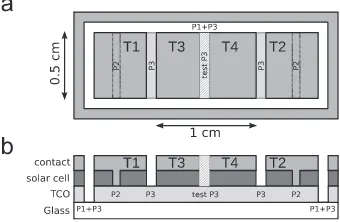
3. Electrical characterization of P3 isolation lines
To characterize test P3 isolation lines we developed the
test structure depicted in Fig. 3. Shown are the top view in
Fig. 3(a) and the cross-sectional view in Fig. 3(b). The test structure has four terminals, T1–4. We first deposit the absorber Fig. 1.Schematic drawing of series interconnection of thin-film silicon solar
module.
Fig. 2.Schematic illustration of pulsed laser patterning of laser lines.
layer on the glass/TCO substrate and two P2 lines are scribed using standard process. After the scribing of the P2 lines the ZnO/ Ag/ZnO back contact layer stack is deposited. After this deposition
we make the standard P3 lines from the glass side (c.f.Fig. 3). In a
final step we isolate the test structure by scribing a line around the test structure removing the entire layer stack, this line is
indicated with ‘‘P1þP3’’ inFig. 3. For details on the standard
process see reference [15]. The last scribe is the test P3 line
scribed with a UV laser from the film side, which separates terminals T3 and T4. However, before we make the test scribe we measure several current/voltage characteristics so we can monitor the changes the scribing of the test line induces.
Before scribing the test P3 line we measure the current/voltage
characteristics between terminals T1 and T2ðJVb
12Þ terminals T1
and T3ðJVb13Þand terminals T2 and T4ðJV
b
24Þ. CharacteristicJV
b 12 reflects the conductivity of the TCO layer before the test scribe.
Characteristics JVb
13 and JVb24 both reflect the current/voltage
characteristics of the solar cell before scribing the test line. After scribing the test P3 line we measure again over terminals
T1 and T2ðJVa
12) terminals T1 and T3ðJVa13) and terminals T2 and
T4 (JVa24). In addition we measure the separation over terminals
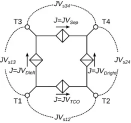
T3 and T4 (JVa34). The resulting four current/voltage characteristics
are modeled with the electrical circuit shown inFig. 4. The model
consists of four Voltage Controlled Current Sources (VCCSs), which are used to model the DC behavior of a two terminal
device with an arbitrary current/voltage (JV) characteristic. The
top component (JVSep) represents the connection between the
back contacts of the two adjacent cells. Ideally, a P3 line separates the back contacts of two adjacent cells and thus the top compo-nent represents a parasitic leakage current that flows directly across the P3 line between the back electrodes. The bottom VCCS
(JVTCO) represents the connection between terminals T1 and T2
via the TCO after the test line. The left and right VCCS components
(JVDleftandJVDright) represent the left solar cell and the right solar
cell, respectively. These current/voltage characteristics include possible damage caused by the scribing of the test P3 line.
We developed an iterative algorithm to separate the electrical characteristics of each individual component in the circuit. First, we assume an initial JV characteristics for each component in the circuit. We then simulate the same four current/voltage charac-teristics we measured using a circuit simulator. The circuit simulator takes tabular voltage/current pairs as input data to form a piece wise linear current/voltage characteristic for each of the VCCS components in the circuit. We then iteratively adapt current/voltage characteristics of each component in the circuit to match the measured and simulated characteristics of the device.
We used the following iterative corrections:
JViþ1,j
where ansin a subscript indicates the current/voltage
character-istics are simulated, the indexirefers to the iteration andJVjis the
j-th current in the tabular set of current/voltage data. The
parameter n is used to enhance convergence of the algorithm
where the largernis the smaller the iterative adaptions to eachJV
characteristic. Typically we initializenwith a large value (e.g. 10)
to avoid oscillations in the iterative adaptions and gradually
reduce the value ofnto 0 as the number of iterations progress.
The algorithm is very simple to implement. We used the
GNUcap circuit simulator for the circuit simulations [19]. The
circuit simulator is called from a GNU Octave [20]script which
implements the iterative algorithm. The method has the advan-tage that we directly use tabular data to describe the current/ voltage characteristics of the components in the circuit, thereby making minimal assumptions about the nature of our devices. However, we did impose one restriction to the current/voltage characteristics of the components, namely that the current is monotonously increasing with applied voltage. This ensures that there is only one unique solution for the currents and voltages in the circuit and generally also improves the numerical stability of the circuit simulation. This restriction is implemented by sorting the current data in ascending order after each iterative refine-ment, without re-ordering the voltages.
We found in working with experimental data that our method initially converges monotonously, i.e. the discrepancy between measured and simulated current/voltage characteristics reduces steadily. However, after the initial convergence the error between simulation and experiment becomes rather erratic, varying see-mingly random from iteration to iteration. However, in many cases the fit can still be improved upon at this stage by letting the algorithm iterate for a while and afterwards selecting the best fit from all previous iterations.
As a last step we compare the device before and after scribing the test P3 line. A change in conductivity of the TCO can be seen
directly from a change inJV12before and after the test line. The
test P3 line may also induce damage to the solar cell in the line and its direct vicinity. We therefore compute the current that flows along one sidewall of the test line (the line has two sidewalls, left and right)
where JVbD is the current/voltage characteristic of the solar cell
before the test line which is computed by averaging the currents
inJVb
13andJVb24. Note that we compare the solar cell before the
test scribe with the sum of the currents through the two solar
cells after the test scribe (i.e., T3þT4) where we neglect the
loss of surface area of the test P3 line as its surface is small
compared to the area of T3þT4 (the area of T3þT4 is 5
101cm2 compared to the area of the test P3 line which is
2:5103cm2). Note that the total leakage current induced by
a P3 line consists ofJsh¼JswþJSep.
Fig. 4.Schematic of the circuit used to model the test device with the terminals T1–4 corresponding to the test structure inFig. 3. Indicated are the four VCCS components,JVTCO,JVDleft,JVDright, andJVSep. Using the circuit the JV curves are simulated over terminals T1 and T2,JVa
s12, T1 and T3,JVas13, T2 and T4,JVas24, and T3
4. Results
In Fig. 5(a) we show a typical measurement of the four current/voltage characteristics after scribing a test P3 line. The typical measurement comes from the overlap number series and
corresponds toO¼5. The characteristicJVa12 has an ohmic
char-acter and exhibits the highest conductivity of the measured JV
characteristics. The JV characteristics JVa13 and JV
a
24 both show
properties of a diode. For voltages above 1.1 V,JVa13andJV
a 24 are approximately the same, whereas at lower bias voltages both exhibit the characteristics of a parallel resistance. The parallel
resistance inJVa13 is smaller than the parallel resistance inJV
a 24.
The separation measured over terminals T3 and T4 (JVa34) is
approximately ohmic and below a voltage of 1.1 V this
character-istic coincides withJVa24.
The dashed lines inFig. 5(a) are the simulated current/voltage
characteristics with the procedure outlined inSection 3. A
con-sistent fit is obtained with an Root-Mean-Square (RMS) relative
error of about 7%. In Fig. 5(b) we show the extracted current/
voltage characteristics of the components in the equivalent circuit of Fig. 4. CharacteristicJVTCO is more or less the same asJVa12.
Furthermore, the left side of solar cell,JVDleftis approximately the
same asJVa
13, indicating thatJVa13is dominated by the left side of
the solar cell. However, the right side of the solar cell,JVDrightdoes
not coincide with JVa24. The separation, JVSep, is approximately
identical to JVa
34. From this it follows that the current in the
characteristic JVa24 below 1.1 V flows predominantly via the
componentsJVSep,JVDleftandJVTCO, rather than directly through
JVDright.
We compare the properties of the test structure before and
after scribing the test line. We find no difference betweenJVa12
andJVb
12(not shown). We therefore conclude the TCO under the
test line is not damaged to the extend it is relevant for the series
connection.Fig. 5(c) shows the diode before the test line,JVbD, and
the diode on the left and right side of the test line,JVDleft and
JVDright, respectively. Using Eq. (6) we determine the sidewall
current density. Note that the sidewall current is the average current flowing along the left and right sidewalls. We cannot distinguish between the left and right sidewall currents because we cannot distinguish between the left and right side of the diode before the scribing of the test line. However, in this case the diode before the test line exhibits lower currents for voltages below 0.8 V than both diodes on the left and right side of the test scribe.
This indicates that the differences between theJVDleftandJVDright
below 0.8 V stem from differences between the left and right side of the sidewall.
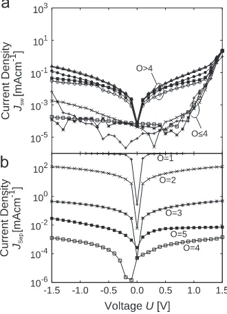
In Fig. 6(a) we show the current density along a sidewalls of the test P3 lines for the overlap number series. In the series we
varied the overlap number fromO¼1 toO¼9. A clear distinction
can be made betweenOr4 and O44. For an overlap number
larger than 4 the sidewall current is considerably larger than for an overlap number below 4 for voltages up to 1.2 V.
Fig. 6(b) shows the separation characteristic. The separation
current density decreases with the overlap number for Or4.
The difference in the separation current density is almost 4 orders
of magnitude between O¼1 and O¼4. For an overlap number
O45 the JVSep cannot be determined accurately because the
current density in JVa
34 is then dominated by the current that
flows viaJVDleft,JVTCO, andJVDright. For this reason we omittedJVSep
fromFig. 6(b) forO45.
The other two series show similar trend to the overlap number series. With increasing pulse power or number of scribes the
Fig. 5.(a) Typical JV measurements and simulation of a test structure. Shown are the four current/voltage measurements (symbols) and the corresponding simu-lated current/voltage characteristics (lines) on the test structure after scribing the test P3 line. The figure corresponds to the P3 line scribed with an overlap number of 5. (b) The components,JVTCO,JVDleft, JVDright, andJVSepas extracted with the iterative scheme of Eqs.(2)–(5). (c) Comparison ofJVDleftandJVDrightwith the solar cell before scribing the test line (JVb
D). From the difference we infer the shunt
induced by the sidewalls of the test line,JVswaccording to Eq.(6).
separation improves. Beyond a certain pulse power or number of scribes, the side wall currents increase. The total parasitic leakage
current induced by a P3 line consists ofJsh¼JswþJSep.
In Fig. 7 we plot Jsh at 1 V for the different series. In all series the leakage current starts high due to insufficient separa-tion of the back contact. For increasing overlap number, pulse power, or number of scribes, the separation improves. An optimum is reached in all series with a leakage current density of 1:8
mA cm
1 for the overlap number series, and 1:5mA cm
1 for both the pulse power and number of scribes series.For comparison, typical short circuit current densities for a-Si:
H=
m
c-Si:H solar modules are in the range of 10–15 mA cm1fora 1 cm width of the cells stripes. Beyond the optimum the sidewall current increases for all series. The side wall currents increase the most for an increasing overlap number. Beyond the optimum the highest leakage current density for the overlap
number series is 0:12 mA cm1, whereas the highest sidewall
leakage current densities beyond the optimum are 17
mA cm
1and 25
mA cm
1for the pulse power and number of scribes series,respectively. For 14 scribes and beyond (marked by open symbols in Fig. 7) the conductivity of the TCO is severely affected after the test scribes, indicating the TCO layer is removed under the P3 line, making these parameters unsuitable for achieving a series connection.
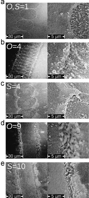
InFig. 8(a) we show SEM images of laser lines produced with
O¼1 andS¼1 (note that the parameters forO¼1 andS¼1 are
identical). The image shows there is much molten and re-solidified material in the line that could be the remains of the
back contact. The optimal laser lines from theOseries (O¼4) and
the scribing times series (S¼4) are shown in Fig. 8(b) and (c),
respectively. The images show less debris in the laser line than in
Fig. 8(a), however some re-solidified material in the line is clearly visible. From optical microscopy images (not shown) it is observed that for these laser lines not all silicon from the laser lines is removed. This re-solidified material is thus probably
silicon. In Fig. 8(d) we show the SEM images of the laser lines
produced withO¼9 and inFig. 8(e) forS¼10. For these lines all
the silicon in the lines is removed. Considering the seemingly flat
surface of the SnOx in the laser lines the SnOx appears to be
molten and re-solidified. Comparing the side of theO¼9 line with
theS¼10 laser line it can be seen that the irregular structures at
the side of the line with O¼9 are wider than for the line with
S¼10.
5. Discussion
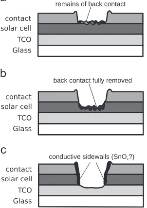
For all the series a low power, a low pulse overlap, or a low number of scribes, lead to a poor separation of the back contacts of the cells. Increasing the power, overlap number or the number of scribes improves the separation. Beyond a certain power, overlap number or the number of scribes, the separation does not improve anymore. Beyond this point the leakage current along the sidewall of the test line increases. We propose the following explanation of the observations. For low power/overlap number/number of scribes the back contact is not completely
removed (seeFig. 9(a)). Increasing total laser energy delivered to
the line to the point where the back contact is completely removed, leads to a good separation of the back contacts (see
Fig. 9(b)). At this point the optimum is reached in terms of a low leakage current. Further increasing the power delivered to the line leads to the complete removal of the silicon layer stack. This complete removal of the silicon leads to an increase in leakage current as the (conductive) sidewalls now connect the front and back electrodes. Indeed optical microscopy images (not shown) confirm that in all series the increase in leakage current beyond the optimum coincides with the silicon layer stack being com-pletely removed from areas within the line. The SEM images for
lines withO¼9 andS¼10 inFig. 8(c) indicate the SnOxin the line
was molten. We therefore speculate that the conductivity of the
sidewalls is in part due to SnOxsplashing out of the laser line over
and onto the sidewalls. The increase in leakage current is strongest for an increasing overlap number, which is likely because with increasing the overlap number the laser power density in the line increases, leading to increasing temperatures in and around the line. For the number of scribes series, however, Fig. 7.The parasitic leakage current density at 1 V (Jsh¼JswþJSep). Note the broken
y-axis and the differenty-axis scales at either side of the break. (a) The leakage current density for the overlap number series, (b) The leakage current density for the pulse power series, and (c) The leakage current density for the number of scribes series. For 14 scribes and beyond the conductivity of the TCO is severely reduced indicating the TCO under the P3 line is removed.
there is a long time between successive scribes leaving ample time for the line to cool down. The higher temperatures for a high overlap number lead to more damage to the sidewalls and/or TCO splashed out of the line.
6. Conclusions
In this paper we investigated laser scribing of P3 isolation lines
for a-Si:H=
m
c-Si:H solar modules from the film side with anano-second pulsed UV laser. We developed a method to char-acterize the electrical properties of the experimental P3 lines. With this method we can distinguish between leakage currents directly across the P3 line, leakage currents along the laser line sidewalls and monitor changes in conductivity of the TCO under-neath the line. We systematically varied scribing parameters for P3 isolation lines with a UV laser incident from the film-side. The properties of the resulting P3 lines where electrically analyzed with the developed method. In addition we examined selected P3 lines using Scanning Electron Microscopy images. We find that the best P3 lines have the back contact fully removed but an incomplete removal of the silicon in the line. If the silicon in the line is fully removed we observe an increase in the leakage current which we could ascribe to currents flowing along the sidewalls of the laser lines. For an incomplete removal of the back contact we observe a leakage current directly across the P3 line.
The best P3 laser line we obtained with the systematic variation of laser parameters exhibits a very low leakage current density of
only 1:5
mA cm
1at 1 V (current per unit laser line length).References
[1] M. Van den Donker, A. Gordijn, H. Stiebig, F. Finger, B. Rech, B. Stannowski, R. Bartl, E. Hamers, R. Schlatmann, G. Jongerden, Flexible amorphous and microcrystalline silicon tandem solar modules in the temporary superstrate concept, Solar Energy Materials and Solar Cells 91 (7) (2007) 572–580. [2] A. Gordijn, M. van den Donker, F. Finger, E. Hamers, G. Jongerden, W. Kessels, R.
Bartl, A. van Mol, J. Rath, B. Rech, et al., Flexiblea-Si=mc-Si tandem modules in the helianthos project, in: Conference Record of the 2006 IEEE 4th World Conference on Photovoltaic Energy Conversion, vol. 2, IEEE, 2006, pp. 1716–1719. [3] J. Rath, Y. Liu, A. Borreman, E. Hamers, R. Schlatmann, G. Jongerden,
R. Schropp, Thin film silicon modules on plastic superstrates, Journal of Non-Crystalline Solids 354 (19) (2008) 2381–2385.
[4] A. Vijh, X. Yang, W. Du, X. Deng, Triple-junction amorphous silicon-based flexible solar minimodule with integrated interconnects, Solar Energy Mate-rials and Solar Cells 90 (16) (2006) 2657–2664.
[5] P. Westin, U. Zimmermann, M. Edoff, Laser patterning of P2 interconnect via in thin-film CIGS PV modules, Solar Energy Materials and Solar Cells 92 (10) (2008) 1230–1235.
[6] P.-O. Westin, U. Zimmermann, M. Ruth, M. Edoff, Next generation inter-connective laser patterning of CIGS thin film modules, Solar Energy Materials and Solar Cells 95 (4) (2011) 1062–1068, http://dx.doi.org/10.1016/ j.solmat.2010.11.015.
[7] I. Zinovik, A. Povitsky, Dynamics of multiple plumes in laser ablation: modeling of the shielding effect, Journal of Applied Physics 100 (2) (2006) 024911, http://dx.doi.org/10.1063/1.2217108.
[8] R. Bartlome, B. Strahm, Y.Y. Sinquin, A. Feltrin, C. Ballif, Laser applications in thin-film photovoltaics, Applied Physics B: Laser and Optics 100 (2) (2009) 427–436.http://dx.doi.org/10.1007/s00340-009-3890-4.
[9] S. Ku, S. Haas, B.E. Pieters, U. Zastrow, A. Besmehn, Q. Ye, U. Rau, Investigation of laser scribing ofa-Si:H from the film side for solar modules using a UV laser with ns pulses, Applied Physics A: Materials Science& Processing 105 (2) (2011) 355–362, http://dx.doi.org/10.1007/s00339-011-6585-8.
[10] S. Lauzurica, J. Garca-Ballesteros, M. Colina, I. Snchez-Aniorte, C. Molpeceres, Selective ablation with UV lasers ofa-Si:H thin film solar cells in direct scribing configuration, Applied Surface Science 257 (12) (2011) 5230–5236, h ttp://dx.doi.org/10.1016/j.apsusc.2010.09.088.
[11] S. Ku, S. Haas, G. Schoepe, B. Pieters, Q. Ye, U. Rau, Direct ablation of ZnO with UV and IR laser for thin film solar modules, Journal of Optoelectronics and Advanced Materials 12 (3) (2010) 616–620.
[12] C. Dunsky, F. Colville, Solid state laser applications in photovoltaic manu-facturing, in: Proceedings of the SPIE, vol. 6871, 2008, p. 87129.
[13] J. Bovatsek, A. Tamhankar, R. Patel, N. Bulgakova, J. Bonse, Effects of pulse duration on the ns-laser pulse induced removal of thin film materials used in photovoltaics, in: Proceedings of the SPIE, vol. 7201, 2009, pp. 720116-1. [14] J. Bovatsek, A. Tamhankar, R. Patel, N. Bulgakova, J. Bonse, Thin film removal
mechanisms in ns-laser processing of photovoltaic materials, Thin Solid Films 518 (10) (2010) 2897–2904.
[15] S. Haas, A. Gordijn, H. Stiebig, High speed laser processing for monolithical series connection of silicon thin-film modules, Progress in Photovoltaics: Research and Applications 16 (3) (2008) 195, http://dx.doi.org/10.1002/ pip.792.
[16] S. Haas, G. Sch ¨ope, C. Zahren, H. Stiebig, Analysis of the laser ablation processes for thin-film silicon solar cells, Applied Physics A 92 (4) (2008) 755, http://dx.doi.org/10.1007/s00339-008-4560-9.
[17] T. Repmann, B. Sehrbrock, C. Zahren, H. Siekmann, B. Rech, Microcrystalline silicon thin film solar modules on glass, Solar Energy Materials and Solar Cells 90 (18) (2006) 3047–3053.
[18] B. Rech, T. Repmann, M. Van den Donker, M. Berginski, T. Kilper, J. H ¨upkes, S. Calnan, H. Stiebig, S. Wieder, Challenges in microcrystalline silicon based solar cell technology, Thin Solid Films 511 (2006) 548–555.
[19]/gnucap.org/S.
[20] J.W. Eaton, GNU Octave Manual, Network Theory Limited, Bristol, United Kingdom, 2002.