arXiv:1709.05852v1 [physics.app-ph] 18 Sep 2017
Z.K. Bishop,∗ A.P. Foster, B. Royall, C. Bentham, M.S. Skolnick, and L.R. Wilson
Department of Physics and Astronomy, University of Sheffield, Sheffield S3 7RH, United Kingdom
E. Clarke
Department of Electronic and Electrical Engineering, University of Sheffield, Sheffield S1 3JD, United Kingdom
The electro-mechanical control of an on-chip GaAs optical router operating at the single-photon level is demonstrated. The routing of single photons is achieved by electro-mechanical tuning of the splitting ratio of an optical beam splitter in the form of a nanobeam waveguide directional coupler (DC). One of the two waveguides forming the DC is located at the free end of a cantilever, which can be displaced vertically downwards by applying an actuation voltage, Vact, between the
cantilever and the substrate. The resulting out-of-plane separation between the waveguides is used to control the splitting ratio of the DC. In the absence ofVact, photons emitted by an InGaAs
self-assembled quantum dot embedded within the fixed arm of the device are split 83:17 between the co-planar through and drop ports of the DC respectively. AsVactis applied the drop port displaces
downwards by over 400 nm causing the splitting ratio to approach 100:0. The single-photon nature of the collected emission is verified with autocorrelation measurements. The proposed system is compact, easy to fabricate and scalable with applications in on-chip photon routing as well as in-situ fine tuning of photonic elements.
Micro-opto-electro-mechanical systems (MOEMS) have been widely studied for a variety of applications in semiconductor integrated photonic circuits. The vast majority of work has been carried out in silicon where on-chip tuning of the optical properties of essential circuit components is possible by displacing them mechanically with the application of an electrostatic field. Lateral displacement has been used in phase modulators, [1, 2] resonance tuning of nanobeam photonic-crystal cavities (PhCCs) [3, 4] and microtoroid resonators. [5] More complicated structures such as comb-drive actuators have also been developed to allow for larger displacements, [6–10] attractive for optical switching applications. [11–14] Recently, scalable out-of-plane actuation methods have also been demonstrated at room temperature based on a cantilever geometry. [15]
MOEMS based on III-V semiconductors are now emerging for applications in quantum information pro-cessing (QIP). Initial work has focused on tuning of PhCC modes into resonance with quantum emitters in order to enhance their emission. In-plane [16] as well as double-membrane out-of-plane actuation methods have been reported, [17–19] both of which offer small dis-placements. Beam splitters, realized on chip using di-rectional couplers (DCs), are another vital component of integrated linear quantum optical circuits, with post-fabrication control of their optical properties likely re-quired for efficient QIP applications. [20, 21] In this con-text, electro-mechanical tuning of DCs has so far only been considered theoretically by Liu et al., [22] using
∗Author to whom correspondence should be addressed. E-mail:
a double-membrane actuation approach. In this Letter we demonstrate the electro-mechanical control of an on-chip beam splitter operating at low temperature using emission from an embedded single photon source. The proposed device is compact, easy-to-fabricate and scal-able [15] with large achievscal-able out-of-plane displacements of over 400 nm.
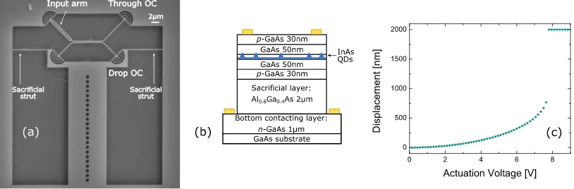
Our device, shown in Fig. 1(a), consists of a nanobeam waveguide DC, which acts as an on-chip optical beam splitter, and a 35µm long and 7.5µm wide cantilever. One arm of the DC is fixed to the bulk of the sam-ple, while the other is located on the free end of the cantilever. Single photons incoming from the input arm of the fixed waveguide are split by the DC between the through and drop ports. This occurs due to evanescent coupling between the waveguides in the 7µm long cou-pling region, in which the in-plane separation of the arms of the DC is nominally 40 nm. The nanobeam waveguides of the DC are designed to be 280 nm wide and 160 nm thick in order to ensure operation in a single (TE) po-larization. Each arm of the DC is terminated with a Bragg output-coupler (OC) to enable out-of-plane col-lection of transmitted photons. The free end of the can-tilever is supported on either side with a 300 nm wide sacrificial strut during sample fabrication and transport. The struts are removed before measurements commence using local laser ablation, releasing the cantilever.
FIG. 1. (a) Top-view scanning electron microscope image of a typical device. The sacrificial struts are removed at low temperature before the opto-electro-mechanical measurements. (b) Schematic diagram of the wafer structure. The position of contacts is marked by gold rectangles. (c) Calculated displacement of the free end of the 35µm long and 7.5µm wide cantilever as actuation voltage is increased.
FIG. 2. Results of the modeling of a directional coupler consisting of 160 nm thick and 280 nm wide waveguides, separated laterally by 80 nm in a 7µm long coupling region. (a) The contour plot shows how the fraction of light evanescently coupled from one channel to the other depends on the wavelength of the transmitted light and the out-of-plane separation between the waveguides. (b) Changes to the signal transmitted (through) in the fixed arm and coupled to the moving arm (drop) as a function of out-of-plane displacement for a wavelength of 910 nm. (c) The overall percentage of light (for a wavelength of 910 nm) transmitted to the through output-coupler increases from 83 % to 100 % as the separation between the waveguides is increased to over 300 nm.
the system. Then-GaAs substrate was isolated from the membrane by a 2µm thick intrinsic Al0.6Ga0.4As layer, which was removed from underneath the device using an HF etch to create the suspended structure. Ni:Au con-tacts were made to the top p- and the bottom n-GaAs layers in order to allow for electro-mechanical control of the cantilever. The row of holes in the center of the de-vice (see Fig. 1(a)) allowed for faster under-etching of the cantilever.
We first present modeling of the electro-mechanical be-havior of the cantilever. Applying an actuation voltage,
Vact, between the cantilever and the substrate results in a capacitive force, which causes the cantilever to deflect towards the substrate. This introduces a vertical out-of-plane separation between the two arms of the DC. Fig-ure 1(c) shows the displacement of the free end of the can-tilever asVact is increased, calculated using an analytical model which determines the displacement for a givenVact by minimizing the total energy of the system (compris-ing strain and electrostatic energies). The model assumes that the cantilever’s vertical displacement is a quadratic function of position along its length. [23] The theoreti-cal maximum controllable displacement of the cantilever
is 1/3 of the initial distance between the cantilever and the substrate,z0. [24] Once this displacement is reached at the so-called pull-in voltage,Vpull, the capacitive force becomes greater than the restoring force and the free end of the cantilever collapses onto the substrate. This intro-duces surface adhesion forces between the cantilever and the substrate. If these forces are smaller than the restor-ing force of the cantilever, the cantilever will be able to lift back up from the substrate atVact < Vpull resulting in a hysteresis behavior. [25, 26] For our systemVpull is calculated to occur at 7.5 V, when the discontinuity in the filled squares curve is observed between the displace-ment of 667 nm and 2000 nm (corresponding toz0/3 and
z0).
FIG. 3. Filtered PL collection map of the device with an overlaid device contour with (a) Vact = 0 V, and (b) Vact =
12.5 V.
could simply be related to the resistance of the contacts, which is not taken into account in the modeling.
Modeling of the optical properties of the DC was per-formed using MIT Photonic-Bands, a freely available eigenmode solver. The results for a DC of the nomi-nal waveguide dimensions discussed above, with a light source located in the fixed arm of the DC, are shown in Fig. 2. The in-plane separation of the arms of the DC in the coupling region was chosen to be 80 nm, so that the modeled optical response is in good quantitative agree-ment with our experiagree-mental results, as we show below. This value is also consistent with that determined from scanning electron microscope measurements of structures with the same designed separations. Depending on the wavelength of the light transmitted through the DC and the out-of-plane separation between its arms the light will be split differently between the two waveguides, vary-ing the percentage of signal exitvary-ing the through OC (see Fig. 2(a)). Figure 2(b) demonstrates this behavior for a single wavelength of 910 nm. When the two arms of the DC are co-planar the DC is undercoupled as 83 % of light is transmitted through the fixed waveguide while only 17 % is coupled to the moving arm, giving a splitting ra-tio (SR) of 83:17. As the out-of-plane separara-tion of the waveguides increases, less light is coupled to the moving arm until at a displacement of about 300 nm the waveg-uides are decoupled and all of the light is routed to the through port, resulting in a SR of 100:0 (see Fig. 2(c)).
The system was studied experimentally using micro-photoluminescence (µ-PL) spectroscopy with spatially resolved excitation and collection in an exchange gas cryostat at 4.2 K using a confocal microscope system. For the measurements of the SR we selected a bright and spectrally isolated QD embedded within the input arm of the DC, emitting at 910.6 nm. The QD was excited from above via the wetting layer using a Ti:Sapphire CW laser emitting at 840 nm. Figure 3 shows twoµ-PL maps, with the device contour overlaid, obtained by raster scanning the collection across the device while spectrally filtering at the QD wavelength. Figure 3(a) was obtained from the device with Vact = 0 V and emission can be seen from both the through and drop OCs. The µ-PL map in Fig. 3(b) was acquired for the device operated with
Vact= 12.5 V, and emission from the drop OC is observed to be heavily suppressed, while that from the through OC
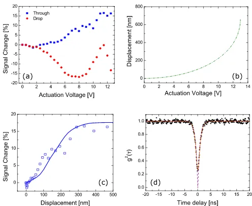
FIG. 4. (a) Measured changes to the QD signal collected from the through and drop OCs independently, as actuation volt-age is increased. The signal is normalized to the total signal recorded from both OCs atVact= 0 V. The peak in the signal
from the drop OC at aboutVact = 11 V is due to changing
optical interference from the moving OC during cantilever actuation. (b) Cantilever displacement as a function of ac-tuation voltage for the measured system, found using Eq. (2) with X = 2650. (c) Experimental results for the through OC from graph (a) as a function of displacement converted from actuation voltage using the relationship in Fig. 4(b). The blue continuous line is the theoretical curve already shown in Fig. 2(b) for ease of comparison. (d) Normalized second-order correlation function obtained by exciting the QD from above and collecting the spectrally filtered PL signal from the input OC. The orange continuous line is a fit to the experimental data (black points), while the dashed purple line represents a fit that takes into account the time response of the measure-ment system.
increases as expected.
To characterize the device at increasing out-of-plane waveguide separation, the routed QD emission was mea-sured simultaneously from the through (fixed) and the drop (moving) OCs using two independent collection paths asVact was increased. The SR for the device at
Vact = 0 V was measured to be 80:20. The absolute per-cent change to the measured signal is shown in Fig. 4(a) for the through and drop OCs separately. The signal is normalized to the total signal collected from both OCs at
Vact= 0 V. The change in the QD emission collected from the through OC increases monotonically until it saturates at 17% for Vact >11 V. The signal at the drop OC de-creases initially as expected, but then recovers and peaks at aboutVact = 11.5 V before decreasing again. This is caused by the downward movement of the drop OC as
In order to directly compare the controlled optical properties of the DC with the modeling (shown in Fig. 2),
Vact was converted to cantilever displacement. To do so, we balanced the capacitive force between the cantilever and the substrate with the restoring force of the can-tilever to obtain:
ǫ0A 2(z0−z)2
V2
act=kz, (1)
wherez0is the initial distance between the cantilever and the substrate (here 2000 nm),zis the displacement of the cantilever, ǫ0 is the permittivity of free space, A is the surface area of the cantilever, andkis a fitting parameter corresponding to an average stiffness of the cantilever. We thus derived the relationship between Vact and the displacement as follows:
Vact=
(z0−z)√z
X , (2)
whereX =pǫ0A/2k nm3/2V-2.
The parameterX for our measured device was found using Vpull = 13 V (the observed pull-in voltage) and the theoretical maximum displacement ofzpull= 667 nm. Equation (2) with X = 2650 was then used to convert
Vactto cantilever displacement and the resulting curve is shown in Fig. 4(b).
This conversion allows us to directly compare the ex-perimentally determined variation in the QD emission routed to the through OC with that calculated using the eigenmode solver (the results of which are presented in Fig. 2). The two curves, presented in Fig. 4(c) as a func-tion of cantilever displacement, are in good agreement with each other demonstrating monotonic increase of the QD signal until saturation at 17 % for displacements of over 300 nm. The achieved displacement of the cantilever was found to be over 400 nm before the pull-in occurs.
We verified the single-photon nature of the emission from this QD by performing an on-chip Hanbury Brown and Twiss experiment, which consists of cross-correlating the photons at the QD wavelength collected by two sep-arate paths from the input OC. The results are shown in Fig. 4(d), with normalizedg(2)(0) = 0.25
±0.02. By deconvolving the experimental data with the temporal re-sponse of our detection system (Gaussian, full-width-at-half-maximum of 874±4 ps) we obtaing(2)(0) = 0
±0.01, which indicates that the source is strongly antibunched. In addition to fine tuning of the integrated optical devices, such as the beam splitter, in situ, the electro-mechanical system presented here is also of interest for optical routing applications. Greater versatility and scal-ability of the system can be achieved through some im-provements to the sample design. [15] Fabricating this structure on ap-i-n-i-ndiode and depositing a third con-tact on the middlen-layer would enable tuning of the QD emission wavelength using the quantum-confined Stark effect [27] at the same time as controlling the beam split-ter electro-mechanically. The operating actuation volt-age could also be decreased by using a thinner AlGaAs sacrificial layer, reducing the initial distance between the two electrodes.
In conclusion, we have demonstrated electro-mechanical control of an on-chip beam splitter operating at low temperature using out-of-plane actuation, with large achievable displacements of over 400 nm. An embedded quantum emitter was used to probe the optical response of the system. The splitting ratio of our on-chip optical beam splitter was tuned from an initial 83:17 at Vact = 0 V (zero displacement) up to 100:0 at Vact = 11 V (300 nm displacement). The proposed device can operate as either a fine tuning element or an optical router and paves the way toward increased control of on-chip single photon devices using compact, easy-to-fabricate and scalable structures for use in III-V semiconductor integrated quantum optical circuits.
This work was funded by EPSRC Grants No. EP/J007544/1 and EP/N031776/1.
[1] K. Van Acoleyen, J. Roels, P. Mechet, T. Claes, D. Van Thourhout, and R. Baers, IEEE Photon. J.4,
779 (2012).
[2] M. Winger, T. D. Blasius, T. P. Alegre, A. H. Safavi-Naeini, S. Meenehan, J. Cohen, S. Stobbe, and O. Painter, Opt. Express19, 24905 (2011).
[3] P. B. Deotare, M. W. McCutcheon, I. W. Frank, M. Khan, and M. Lonˇcar, Appl. Phys. Lett.95, 031102
(2009).
[4] I. W. Frank, P. B. Deotare, M. W. McCutcheon, and M. Lonˇcar, Opt. Express18, 8705 (2010).
[5] C. G. Baker, C. Bekker, D. L. McAuslan, E. Sheridan, and W. P. Bowen, Opt. Express14, 20400 (2016).
[6] R. Legtenberg, A. W. Groeneveld, and M. Elwenspoek, J. Micromech. Microeng.6, 320 (1996).
[7] G. Zhou and P. Dowd, J. Micromech. Microeng.13, 178
(2003).
[8] X. Chew, G. Zhou, F. S. Chau, J. Deng, X. Tang, and Y. C. Loke, Opt. Lett.35, 2517 (2010).
[9] X. Chew, G. Zhou, H. Yu, F. S. Chau, J. Deng, L. Y. C., and X. Tang, Opt. Express18, 22232 (2010).
[10] P. Shi, G. Zhou, J. Deng, F. Tian, and F. S. Chau, Sci. Rep.5, 14379 (2015).
[11] E. Bulgan, Y. Kanamori, and K. Hane, Appl. Phys. Lett.
92, 101110 (2008).
[12] Y. Akihama, Y. Kanamori, and K. Hane, Opt. Express
[16] R. Ohta, Y. Ota, H. Takagi, N. Kumagai, K. Tanabe, S. Ishida, S. Iwamoto, and Y. Arakawa, Jpn. J. Appl. Phys.52, 04CG01 (2013).
[17] L. Midolo, P. J. van Veldhoven, M. A. D¨undar, R. N¨otzel, and A. Fiore, Appl. Phys. Lett.98, 211120 (2011).
[18] L. Midolo, S. N. Yoon, F. Pagliano, T. Xia, F. W. M. van Otten, M. Lermer, S. H¨ofling, and A. Fiore, Opt. Express20(2012).
[19] M. Petruzzella, T. Xia, F. Pagliano, S. Birindelli, L. Mi-dolo, Z. Zobenica, L. H. Li, E. H. Linfield, and A. Fiore, Appl. Phys. Lett.107(2015).
[20] E. Knill, R. Laflamme, and G. J. Milburn, Nature409,
46 (2001).
[21] H. J. Kimble, Nature453, 1023 (2008).
[22] T. Liu, F. Pagliano, and A. Fiore, Opt. Express 25,
10166 (2017).
[23] S. Tsuchitani and R. Kaneko, T. IEE Japan 118, 6
(1998).
[24] L. Midolo and A. Fiore, IEEE J. Quant. Electron.50,
404 (2014).
[25] J. O. Lee, Y.-H. Song, M.-W. Kim, M.-H. Kang, J.-S. Oh, H.-H. Yang, and J. B. Yoon, Nat. Nanotechnol.8,
36 (2013).
[26] O. Buchnev, N. Podoliak, T. Frank, M. Kaczmarek, L. Jiang, and V. A. Fedotov, ACS Nano 10, 11519
(2016).