H
Op Amp History
1
Op Amp Basics
1
Introduction
2
Op Amp Topologies
3
Op Amp Structures
4
Op Amp Specifications
5
Precision Op Amps
6
High Speed Op Amps
2
Specialty Amplifiers
3
Using Op Amps with Data Converters
4
Sensor Signal Conditioning
5
Analog Filters
6
Signal Amplifiers
CHAPTER 1: OP AMP BASICS
James Bryant, Walt Jung, Walt Kester
Within Chapter 1, discussions are focused on the basic aspects of op amps. After a brief introductory section, this begins with the fundamental topology differences between the two broadest classes of op amps, those using voltage feedback and current feedback. These two amplifier types are distinguished more by the nature of their internal circuit topologies than anything else. The voltage feedback op amp topology is the classic structure, having been used since the earliest vacuum tube based op amps of the 1940 and 1950’s, through the first IC versions of the 1960’s, and includes most op amp models produced today. The more recent IC variation of the current feedback amplifier has come into popularity in the mid-to-late 1980’s, when higher speed IC op amps were developed. Factors distinguishing these two op amp types are discussed at some length.
Details of op amp input and output structures are also covered in this chapter, with emphasis how such factors potentially impact application performance. In some senses, it is logical to categorize op amp types into performance and/or application classes, a process that works to some degree, but not altogether.
In practice, once past those obvious application distinctions such as "high speed" versus "precision," or "single" versus "dual supply," neat categorization breaks down. This is simply the way the analog world works. There is much crossover between various
classes, i.e., a high speed op amp can be either single or dual-supply, or it may even fit as a precision type. A low power op amp may be precision, but it need not necessarily be single-supply, and so on. Other distinction categories could include the input stage type, such as FET input (further divided into JFET or MOS, which in turn are further divided into NFET or PFET and PMOS and NMOS, respectively), or bipolar (further divided into NPN or PNP). Then, all of these categories could be further described in terms of the type of input (or output) stage used.
So, it should be obvious that categories of op amps are like an infinite set of analog gray scales; they don’t always fit neatly into pigeonholes, and we shouldn’t expect them to. Nevertheless, it is still very useful to appreciate many of the aspects of op amp design that go into the various structures, as these differences directly influence the optimum op amp choice for an application. Thus structure differences are application drivers, since we choose an op amp to suit the nature of the application, for example single-supply.
SECTION 1: INTRODUCTION
Walt Jung
As a precursor to more detailed sections following, this introductory chapter portion considers the most basic points of op amp operation. These initial discussions are
oriented around the more fundamental levels of op amp applications. They include: Ideal Op Amp Attributes, Standard Op Amp Feedback Hookups, The Non-Ideal Op Amp, Op amp Common Mode Dynamic Range(s), the various Functionality Differences of Single and Dual-Supply Operation, and the Device Selection process.
Before op amp applications can be developed, some first requirements are in order. These include an understanding of how the fundamental op amp operating modes differ, and whether dual-supply or single-supply device functionality better suits the system under consideration. Given this, then device selection can begin and an application developed.
Figure 1-1: The ideal op amp and its attributes
First, an operational amplifier (hereafter simply op amp) is a differential input, single ended output amplifier, as shown symbolically in Figure 1-1. This device is an amplifier intended for use with external feedback elements, where these elements determine the resultant function, or operation. This gives rise to the name "operational amplifier," denoting an amplifier that, by virtue of different feedback hookups, can perform a variety of operations.1 At this point, note that there is no need for concern with any actual
technology to implement the amplifier. Attention is focused more on the behavioral nature of this building block device.
An op amp processes small, differential mode signals appearing between its two inputs, developing a single ended output signal referred to a power supply common terminal. Summaries of the various ideal op amp attributes are given in the figure. While real op amps will depart from these ideal attributes, it is very helpful for first-level understanding of op amp behavior to consider these features. Further, although these initial discussions
1 The actual naming of the operational amplifier occurred in the classic Ragazinni, et al paper of 1947 (see
Reference 1). However analog computations using op amps as we know them today began with the work of
OP AMP
OP AMP INPUTS:
OP AMP OUTPUT:
High Input Impedance
Low Bias Current
Respond to Differential Mode Voltages
Ignore Common Mode Voltages
Low Source Impedance IDEAL OP AMP ATTRIBUTES:
Infinite Differential Gain
Zero Common Mode Gain
Zero Offset Voltage
Zero Bias Current
OUTPUT POSITIVE SUPPLY
NEGATIVE SUPPLY INPUTS
(+)
talk in idealistic terms, they are also flavored by pointed mention of typical "real world" specifications— for a beginning perspective.
It is also worth noting that this op amp is shown with five terminals, a number that happens to be a minimum for real devices. While some single op amps may have more than five terminals (to support such functions as frequency compensation, for example), none will ever have less. By contrast, those elusive ideal op amps don’t require power, and symbolically function with just four pins. 1
Ideal Op Amp Attributes
An ideal op amp has infinite gain for differential input signals. In practice, real devices will have quite high gain (also called open-loop gain) but this gain won’t necessarily be precisely known. In terms of specifications, gain is measured in terms of VOUT/VIN, and is
given in V/V, the dimensionless numeric gain. More often however, gain is expressed in decibel terms (dB), which is mathematically dB = 20 • log (numeric gain). For example, a numeric gain of 1 million (106 V/V) is equivalent to a 120 dB gain. Gains of 100-130 dB are common for precision op amps, while high speed devices may have gains in the 60-70 dB range.
Also, an ideal op amp has zero gain for signals common to both inputs, that is, common mode (CM) signals. Or, stated in terms of the rejection for these common mode signals, an ideal op amp has infinite CM rejection (CMR). In practice, real op amps can have CMR specifications of up to 130 dB for precision devices, or as low as 60-70 dB for some high speed devices.
The ideal op amp also has zero offset voltage (VOS=0), and draws zero bias current (IB=0)
at both inputs. Within real devices, actual offset voltages can be as low as a µV or less, or as high as several mV. Bias currents can be as low as a few fA, or as high as several µA. This extremely wide range of specifications reflects the different input structures used within various devices, and is covered in more detail later in this chapter.
The attribute headings within Figure 1-1 for INPUTS and OUTPUT summarize the above concepts in more succinct terms. In practical terms, another important attribute is the concept of low source impedance, at the output. As will be seen later, low source impedance enables higher useful gain levels within circuits.
To summarize these idealized attributes for a signal-processing amplifier, some of the traits might at first seem strange. However, it is critically important to reiterate that op amps simply are never intended for use without overall feedback! In fact, as noted, the connection of a suitable external feedback loop defines the closed-loop amplifier’s gain and frequency response characteristics.
Note also that all real op amps have a positive and negative power supply terminal, but rarely (if ever) will they have a separate ground connection. In practice, the op amp
output voltage becomes referred to a power supply common point. Note: This key point is further clarified with the consideration of typically used op amp feedback networks.
The basic op amp hookup of Figure 1-2 below applies a signal to the (+) input, and a (generalized) network delivers a fraction of the output voltage to the (−) input terminal. This constitutes feedback, with the op amp operating in closed-loop fashion. The
feedback network (shown here in general form) can be resistive or reactive, linear or non-linear, or any combination of these. More detailed analysis will show that the circuit gain characteristic as a whole follows the inverse of the feedback network transfer function.
Figure 1-2: A generalized op amp circuit with feedback applied
The concept of feedback is both an essential and salient point concerning op amp use. With feedback, the net closed-loop gain characteristics of a stage such as Fig. 1-2 become primarily dependent upon a set of external components (usually passive). Thus behavior is less dependent upon the relatively unstable amplifier open-loop characteristics.
Note that within Figure 1-2, the input signal is applied between the op amp (+) input and a common or reference point, as denoted by the ground symbol. It is important to note that this reference point is also common to the output and feedback network. By
definition, the op amp stage’s output signal appears between the output terminal/feedback network input, and this common ground. This single relevant fact answers the "Where is the op amp grounded?" question so often asked by those new to the craft. The answer is simply that it is grounded indirectly, by virtue of the commonality of its input, the feedback network, and the power supply, as is shown within Fig. 1-2.
To emphasize how the input/output signals are referenced to the power supply, dual supply connections are shown dotted, with the ± power supply midpoint common to the input/output signal ground. But do note, while all op amp application circuits may not show full details of the power supply connections, every real circuit will always use
INPUT
FEEDBACK NETWORK
Standard Op Amp Feedback Hookups
Virtually all op amp feedback connections can be categorized into just a few basic types. These include the two most often used, non-inverting and inverting voltage gain stages, plus a related differential gain stage.Having discussed above just the attributes of the ideal op amp, at this point it is possible to conceptually build basic gain stages. Using the concepts of infinite gain, zero input offset voltage, zero bias current, etc., standard op amp feedback hookups can be devised. For brevity, a full mathematical development of these concepts isn'tincluded below (but this follows in a subsequent section). The
end-of-section references also include such developments.
The Non-inverting Op Amp Stage
The op amp non-inverting gain stage, also known as a voltage follower with gain, or simply voltage follower, is shown below in Figure 1-3.
Figure 1-3: The non-inverting op amp stage (voltage follower)
This op amp stage processes the input VIN by a gain of G, so a generalized expression for
gain is:
IN OUT
V V G =
Eq. 1-1
Feedback network resistances RF and RG set the stage gain of the follower. For an ideal
op amp, the gain of this stage is:
G G F
R R R G = +
Eq. 1-2
For clarity, these expressions are also included in the figure. Comparison of this figure and the more general Figure 1-2 shows RF and RG here as a simple feedback network,
returning a fraction of VOUT to the op amp (−) input (note that some texts may show the
more general symbols ZF and ZG for these feedback components— both are correct,
depending upon the specific circumstances).
VIN VOUT
OP AMP
RF
RG
In fact, we can make some useful general points about the network RF – RG. We will
define the transfer expression of the network as seen from the top of RF to the output
across RG as β. Note that this usage is a general feedback network transfer term, not to be
confused with bipolar transistor forward gain. β can be expressed mathematically as:
G F
G
R R
R
β
+
=
Eq. 1-3
So, the feedback network returns a fraction of VOUT to the op amp (–) input. Considering
the ideal principles of zero offset and infinite gain, this allows some deductions on gain to be made. The voltage at the (–) input is forced by the op amp's feedback action to be equal to that seen at the (+) input, VIN. Given this relationship, it is relatively easy to
work out the ideal gain of this stage, which in fact turns out to be simply the inverse of β. This is apparent from a comparison of equations 1-2 and 1-3.
Thus an ideal non-inverting op amp stage gain is simply equal to 1/β, or:
β
1
G = Eq. 1-4
This non-inverting gain configuration is one of the most useful of all op amp stages, for several reasons. Because VIN sees the op amp’s high impedance (+) input, it provides an
ideal interface to the driving source. Gain can easily be adjusted over a wide range via RF
and RG, with virtually no source interaction.
A key point is the interesting relationship concerning RF and RG. Note that to satisfy the
conditions of Equation 1-2, only their ratio is of concern. In practice this means that stable gain conditions can exist over a range of actual RF – RG values, so long as they
provide the same ratio.
If RF is taken to zero and RG open, the stage gain becomes unity, and VOUT is then exactly
equal to VIN. This special non-inverting gain case is also called a unity gain follower, a
stage commonly used for buffering a source.
Note that this op amp example shows only a simple resistive case of feedback. As mentioned, the feedback can also be reactive, i.e., ZF, to include capacitors and/or
inductors. In all cases however, it must include a DC path, if we are to assume the op amp is being biased by the feedback (which is usually the case).
To summarize some key points on op amp feedback stages, we paraphrase from Reference 2 the following statements, which will always be found useful:
The summing point idiom is probably the most used phrase of the aspiring analog artificer, yet the least appreciated. In general, the inverting (−) input is called the
summing point, while the non-inverting (+) input is represented as the reference terminal. However, a vital concept is the fact that, within linear op amp applications,
The Inverting Op Amp Stage
The op amp inverting gain stage, also known simply as the inverter, is shown in Figure 1-4. As can be noted by comparison of Figures 1-3 and 1-4, the inverter can be viewed as similar to a follower, but with a transposition of the input voltage VIN. In the inverter the
signal is applied to RG of the feedback network, and the op amp (+) input is grounded.
The feedback network resistances, RF and RG set the stage gain of the inverter. For an
ideal op amp, the gain of this stage is:
G F
R R
G =− Eq. 1-5
For clarity, these expressions are again included in the figure. Note that a major
difference between this stage and the non-inverting counterpart is the input-to-output sign reversal, denoted by the minus sign in Equation 1-5. Like the follower stage, applying ideal op amp principles and some basic algebra can derive the gain expression of Eq. 1-5.
Figure 1-4: The inverting op amp stage (inverter)
The inverting configuration is also one of the more useful op amp stages. Unlike a non-inverting stage however, the inverter presents a relatively low impedance input for VIN,
i.e., the value of RG. This factor provides a finite load to the source. While the stage gain
can in theory be adjusted over a wide range via RF and RG, there is a practical limitation
imposed at high gain, when RG becomes relatively low. If RF is zero, the gain becomes
zero. RF can also be made variable, in which case the gain is linearly variable over the
dynamic range of the element used for RF. As with the follower gain stage, the gain is
ratio dependent, and is relatively insensitive to the exact RF and RG values.
The inverter’s gain behavior, due to the principles of infinite op amp gain, zero input offset, and zero bias current, gives rise to an effective node of zero voltage at the (−) input. The input and feedback currents sum at this point, which logically results in the term summing point. It is also called a virtual ground, because of the fact it will be at the same potential as the grounded reference input.
VIN
= - RF/RG
VOUT OP AMP
RF RG
Note that, technically speaking, all op amp feedback circuits have a summing point, whether they are inverters, followers, or a hybrid combination. The summing point is always the feedback junction at the (–) input node, as shown in Fig. 1-4. However in follower type circuits this point isn’t a virtual ground, since it follows the (+) input.
A special gain case for the inverter occurs when RF = RG, which is also called a unity
gain inverter. This form of inverter is commonly used for generating complementary VOUT signals, i.e., VOUT = −VIN. In such cases it is usually desirable to match RF to RG
accurately, which can readily be done by using a well-specified matched resistor pair.
A variation of the inverter is the inverting summer, a case similar to Figure 1-4, but with input resistors RG2, RG3, etc (not shown). For a summer individual input resistors are
connected to additional sources VIN2, VIN3, etc., with their common node connected to the
summing point. This configuration, called a summing amplifier, allows linear input current summation in RF.1 VOUT is proportional to an inverse sum of input currents.
The Differential Op Amp Stage
The op amp differential gain stage (also known as a differential amplifier, or subtractor) is shown in Figure 1-5.
Figure 1-5: The differential amplifier stage (subtractor)
Paired input and feedback network resistances set the gain of this stage. These resistors, RF –RG and RF′ – RG′, must be matched as noted, for proper operation. Calculation of
individual gains for inputs V1 and V2 and their linear combination derives the stage gain.
Note that the stage is intended to amplify the difference of voltages V1 and V2, so the net
input is VIN = V1 – V2. The general gain expression is then:
2 1-V
V
OUT
V G =
Eq. 1-6
1The very first general-purpose op amp circuit is described by Karl Swartzel in Reference 3, and is titled
"Summing Amplifier". This amplifier became a basic building block of the M9 gun director computer and fire control system used by Allied Forces in World War II. It also influenced many vacuum tube op amp
VIN = V1 - V2
= RF/RG
VOUT OP AMP
RF RG
G = VOUT/VIN
RF'
V2
V1
for RF'/RG' ≡ RF/RG
G1 G2
For an ideal op amp and the resistor ratios matched as noted, the gain of this differential stage from VIN to VOUT is:
G
R
F
R G =
Eq. 1-7
The great fundamental utility that an op amp stage such as this allows is the property of rejecting voltages common to V1-V2, i.e., common-mode (CM) voltages. For example, if
noise voltages appear between grounds G1 and G2, the noise will be suppressed by the common-mode rejection (CMR) of the differential amp. The CMR is however only as good as the matching of the resistor ratios allows, so in practical terms it implies
precisely trimmed resistor ratios are necessary. Another disadvantage of this stage is that the resistor networks load the V1-V2 sources, potentially leading to additional errors.
The Non-Ideal Op Amp— Static Errors Due to Finite Amplifier Gain
One of the most distinguishing features of op amps is their staggering magnitude of DC voltage gain. Even the least expensive devices have typical voltage gains of 100,000 (100dB), while the highest performance precision bipolar and chopper stabilized units can have gains as high 10,000,000 (140dB), or more. Negative feedback applied around this much voltage gain readily accomplishes the virtues of closed-loop performance, making the circuit dependent only on the feedback components.
Figure 1-6: Non-ideal op amp stage for gain error analysis
As noted above in the discussion of ideal op amp attributes, the behavioral assumptions follow from the fact that negative feedback, coupled with high open-loop gain, constrains the amplifier input error voltage (and consequently the error current) to infinitesimal values. The higher this gain, the more valid these assumptions become.
But in reality, op amps do have finite gain, and errors exist in practical circuits. The op amp gain stage of Figure 1-6 will be used to illustrate how these errors impact
performance. In this circuit the op amp is ideal except for the finite open-loop DC voltage gain, A, which is usually stated as AVOL.
β network
VOUT
OP AMP * ZF ZG
VIN
G1 G2
Noise Gain (NG)
The first aid to analyzing op amps circuits is to differentiate between noise gain and
signal gain. We have already discussed the differences between non-inverting and inverting stages as to their signal gains, which are summarized in Equations 1-2 and 1-4, respectively. But, as can be noticed from Fig. 1-6, the difference between an inverting and non-inverting stage can be as simple as just where the reference ground is placed. For a ground at point G1, the stage is an inverter; conversely, if the ground is placed at point G2 (with no G1) the stage is non-inverting.
Note however that in terms of the feedback path, there are no real differences. To make things more general, the resistive feedback components previously shown are replaced here with the more general symbols ZF and ZG, otherwise they function as before. The
feedback attenuation, β, is the same for both the inverting and non-inverting stages:
F
Noise gain can now be simply defined as: The inverse of the net feedback attenuation from the amplifier output to the feedback input. In other words, the inverse of the β network transfer function. This can ultimately be extended to include frequency dependence (covered later in this chapter). Noise gain can be abbreviated as NG.
As noted, the inverse of β is the ideal non-inverting op amp stage gain. Including the effects of finite op amp gain, a modified gain expression for the non-inverting stage is:
where GCL is the finite-gain stage's closed-loop gain, and AVOL is the op amp open-loop
voltage gain for loaded conditions.
It is important to note that this expression is identical to the ideal gain expression of Eq. 1-4, with the addition of the bracketed multiplier on the right side. Note also that this right-most term becomes closer and closer to unity, as AVOL approaches infinity.
Accordingly, it is known in some textbooks as the error multiplier term, when the expression is shown in this form. 1
It may seem logical here to develop another finite gain error expression for an inverting amplifier, but in actuality there is no need. Both inverting and non-inverting gain stages have a common feedback basis, which is the noise gain. So Eq. 1-9 will suffice for gain error analysis for both stages. Simply use the β factor as it applies to the specific case.
1 Some early discussions of this finite gain error appear in References 4 and 5. Terman uses the open-loop
It is useful to note some assumptions associated with the rightmost error multiplier term
This in turn leads to an estimation of the percentage error, ε, due to finite gain AVOL:
β
The closed-loop gain error predicted by these equations isn't in itself tremendously important, since the ratio ZF/ZG could always be adjusted to compensate for this error.
But note however that closed-loop gain stability is a very important consideration in most applications. Closed-loop gain instability is produced primarily by variations in open-loop gain due to changes in temperature, loading, etc.
β
insofar as the effect on closed-loop gain. This improvement in closed-loop gain stability is one of the important benefits of negative feedback.
Loop gain
The product AVOLβ which occurs in the above equations, is called loop gain, a
well-known term in feedback theory. The improvement in closed-loop performance due to negative feedback is, in nearly every case, proportional to loop gain.
The term "loop gain" comes from the method of measurement. This is done by breaking the closed feedback loop at the op amp output, and measuring the total gain around the loop. In Fig. 1-6 for example, this could be done between the amplifier output and the feedback path (see arrows). Approximately, closed-loop output impedance, linearity,
and gain instability errors reduce by the factor AVOL , β with the use of negative feedback.
Another useful approximation is developed as follows. A rearrangement of Eq. 1-9 is:
Consequently, in a given feedback circuit the loop gain, AVOLβ, is approximately the
numeric ratio (or difference, in dB) of the amplifier open-loop gain to the circuit closed-loop gain.
This loop gain discussion emphasizes that indeed, loop gain is a very significant factor in predicting the performance of closed-loop operational amplifier circuits. The open-loop gain required to obtain an adequate amount of loop gain will, of course, depend on the desired closed-loop gain.
For example, using Equation 1-14, an amplifier with AVOL = 20,000 will have an AVOLβ
≈ 2000 for a closed-loop gain of 10, but the loop gain will be only 20 for a closed-loop gain of 1000. The first situation implies an amplifier-related gain error the order of ≈0.05%, while the second would result in about 5% error. Obviously, the higher the required gain, the greater will be the required open-loop gain to support an AVOLβ for a
given accuracy.
Frequency Dependence of Loop Gain
Thus far, it has been assumed that amplifier open-loop gain is independent of frequency. Unfortunately, this isn't the case at all. Leaving the discussion of the effect of open-loop response on bandwidth and dynamic errors until later, let us now investigate the general effect of frequency response on loop gain and static errors.
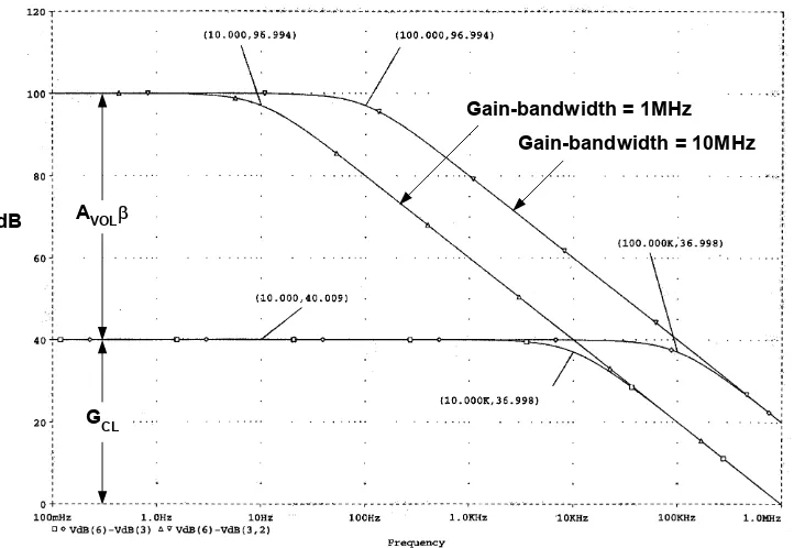
Figure 1-7: Op amp closed-loop gain and loop gain interactions with typical open-loop responses
The open-loop frequency response for a typical operational amplifier with superimposed closed-loop amplifier response for a gain of 100 (40dB), illustrates graphically these results, in Figure 1-7. In these Bode plots, subtraction on a logarithmic scale is equivalent
AVOLβ dB
GCL
to normal division of numeric data. 1 Today, op amp open-loop gain and loop gain parameters are typically given in dB terms, thus this display method is convenient.
A few key points evolve from this graphic figure, which is a simulation involving two hypothetical op amps, both with a DC/low frequency gain of 100dB (100kV/V). The first has a gain-bandwidth of 1MHz, while the gain-bandwidth of the second is 10MHz.
•
The open-loop gain AVOL for the two op amps is noted by the two curves marked 1and 10MHz, respectively. Note that each has a –3dB corner frequency associated with it, above which the open-loop gain falls at 6dB/octave. These corner frequencies are marked at 10 and 100Hz, respectively, for the two op amps.
•
At any frequency on the open-loop gain curve, the numeric product of gain AVOL andfrequency, f, is a constant (10,000V/V at 100Hz equates to 1MHz). This, by definition, is characteristic of a constant gain-bandwidth product amplifier. All
voltage feedback op amps behave in this manner.
•
AVOLβ in dB is the difference between open-loop gain and closed-loop gain, asplotted on log-log scales. At the lower frequency point marked, AVOLβ is thus 60dB.
•
AVOLβ decreases with increasing frequency, due to the decrease of AVOL above theopen-loop corner frequency. At 100Hz for example, the 1MHz gain-bandwidth amplifier shows an AVOLβ of only 80–40 = 40dB.
•
AVOLβ also decreases for higher values of closed-loop gain. Other, higher closed-loopgain examples (not shown) would decrease AVOLβ to less than 60dB at low
frequencies.
•
GCL depends primarily on the ratio of the feedback components, ZF and ZG, and isrelatively independent of AVOL (apart from the errors discussed above, which are
inversely proportional to AVOLβ). In this example 1/β is 100, or 40dB, and is so
marked at 10Hz. Note that GCL is flat with increasing frequency, up until that
frequency where GCL intersects the open-loop gain curve, and AVOLβ drops to zero.
•
At this point where the closed-loop and open-loop curves intersect, the loop gain is by definition zero, which implies that beyond this point there is no negative feedback. Consequently, closed-loop gain is equal to open-loop gain for further increases in frequency.•
Note that the 10MHz gain-bandwidth op amp allows a 10× increase in closed-loop bandwidth, as can be noted from the –3dB frequencies; that is 100kHz versus 10kHz for the 10MHz versus the 1MHz gain-bandwidth op amp.
1The log-log displays of amplifier gain (and phase) versus frequency are called Bode plots. This graphic
Fig. 1-7 illustrates that the high open-loop gain figures typically quoted for op amps can be somewhat misleading. As noted, beyond a few Hz, the open-loop gain falls at
6dB/octave. Consequently, closed-loop gain stability, output impedance, linearity and other parameters dependent upon loop gain are degraded at higher frequencies. One of the reasons for having DC gain as high as 100dB and bandwidth as wide as several MHz, is to obtain adequate loop gain at frequencies even as low as 100Hz.
A direct approach to improving loop gain at high frequencies other than by increasing open-loop gain is to increase the amplifier open-loop bandwidth. Figure 1-7 shows this in terms of two simple examples. It should be borne in mind however that op amp gain-bandwidths available today extend to the hundreds of MHz, allowing video and high- speed communications circuits to fully exploit the virtues of feedback.
Op amp Common Mode Dynamic Range(s)
As a point of departure from the idealized circuits above, some practical basic points are now considered. Among the most evident of these is the allowable input and output dynamic ranges afforded in a real op amp. This obviously varies with not only the specific device, but also the supply voltage. While we can always optimize this
performance point with device selection, more fundamental considerations come first.
Figure 1-8: Op amp input and output common mode ranges
Any real op amp will have a finite voltage range of operation, at both input and output. In modern system designs, supply voltages are dropping rapidly, and 3-5V total supply voltages are now common. This is a far cry from supply systems of the past, which were typically ±15V (30V total). Obviously, if designs are to accommodate a 3-5V supply, careful consideration must be given to maximizing dynamic range, by choosing a correct device. Choosing a device will be in terms of exact specifications, but first and foremost it should be in terms of the basic topologies used within it.
Output Dynamic Range
Figure 1-8 above is a general illustration of the limitations imposed by input and output dynamic ranges of an op amp, related to both supply rails. Any op amp will always be powered by two supply potentials, indicated by the positive rail, +VS, and the negative
OP AMP +VS
-VS (OR GROUND)
VSAT(HI)
VSAT(LO)
VCM(HI)
VCM(LO)
rail, -VS. We will define the op amp’s input and output CM range in terms of how closely
it can approach these two rail voltage limits.
At the output, VOUT has two rail-imposed limits, one high or close to +VS, and one low,
or close to –VS. Going high, it can range from an upper saturation limit of +VS –VSAT(HI)
as a positive maximum. For example if +VS is 5V, and VSAT(HI) is 100mV, the upper VOUT
limit or positive maximum is 4.9V. Similarly, going low it can range from a lower saturation limit of –VS + VSAT(LO). So, if –VS is ground (0V) and VSAT(LO) is 50mV, the
lower limit of VOUT is simply 50mV.
Obviously, the internal design of a given op amp will impact this output CM dynamic range, since, when so necessary, the device itself must be designed to minimize both VSAT(HI) and VSAT(LO), so as to maximize the output dynamic range. Certain types of op
amp structures are so designed, and these are generally associated with designs expressly for single-supply systems. This is covered in detail later within the chapter.
Input Dynamic Range
At the input, the CM range useful for VIN also has two rail-imposed limits, one high or
close to +VS, and one low, or close to –VS. Going high, it can range from an upper CM
limit of +VS - VCM(HI) as a positive maximum. For example, again using the +VS = 5V
example case, if VCM(HI) is 1V, the upper VIN limit or positive CM maximum is +VS –
VCM(HI), or 4V.
Figure 1-9: A graphical display of op amp input common mode range
Figure 1-9 above illustrates by way of a hypothetical op amp’s data how VCM(HI) could be
specified, as shown in the upper curve. This particular op amp would operate for VCM
inputs lower than the curve shown.
In practice the input CM range of real op amps is typically specified as a range of
voltages, not necessarily referenced to +VS or -VS. For example, a typical ±15V operated
dual supply op amp would be specified for an operating CM range of ±13V. Going low, there will also be a lower CM limit. This can be generally expressed as -VS + VCM(LO),
which would appear in a graph such as Fig. 1-9 as the lower curve, for VCM(LO). If this
were again a ±15V part, this could represent typical performance.
VCM(HI)
To use a single-supply example, for the –VS = 0V case, if VCM(LO) is 100mV, the lower
CM limit will be 0V + 0.1V, or simply 0.1V. Although this example illustrates a lower CM range within 100mV of –VS, it is actually much more typical to see single-supply
devices with lower or upper CM ranges, which include the supply rail.
In other words, VCM(LO) or VCM(HI) is 0V. There are also single-supply devices with CM
ranges that include both rails. More often than not however, single-supply devices will not offer graphical data such as Fig. 1-9 for CM limits, but will simply cover
performance with a tabular range of specified voltage.
Functionality Differences of Dual-Supply and Single-Supply Devices
There are two major classes of op amps, the choice of which determines how well the selected part will function in a given system. Traditionally, many op amps have been designed to operate on a dual power supply system, which has typically been ±15V. This custom has been prevalent since the earliest IC op amps days, dating back to the mid-sixties. Such devices can accommodate input/output ranges of ±10V (or slightly more), but when operated on supplies of appreciably lower voltage, for example ±5V or less, they suffer either loss of performance, or simply don’t operate at all. This type of device is referenced here as a dual-supply op amp design. This moniker indicates that it
performs optimally on dual voltage systems only, typically ±15V. It may or may not also work at appreciably lower voltages.
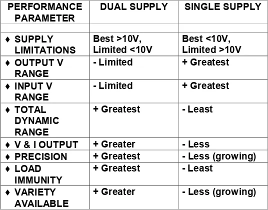
Figure 1-10: Comparison of relative functional performance differences between single and dual-supply op amps
Figure 1-10 above illustrates in a broad overview the relative functional performance differences that distinguish the dual-supply vs. single-supply op amp classes. This table is arranged to illustrate various general performance parameters, with an emphasis on the contrast between single and dual-supply devices. Which particular performance area is more critical will determine what type of device will be the better system choice.
PERFORMANCE PARAMETER
DUAL SUPPLY SINGLE SUPPLY
♦SUPPLY LIMITATIONS
Best >10V, Limited <10V
Best <10V, Limited >10V
♦OUTPUT V RANGE
- Limited + Greatest
♦INPUT V RANGE
- Limited + Greatest
♦TOTAL DYNAMIC RANGE
+ Greatest - Least
♦V & I OUTPUT + Greater - Less
♦PRECISION + Greatest - Less (growing)
♦LOAD IMMUNITY
+ Greatest - Least
♦VARIETY AVAILABLE
More recently, with increasing design attention to lower overall system power and the use of single rail power, the single-supply op amp has come into vogue. This has not been without good reason, as the virtues of using single supply rails can be quite compelling. A review of Fig. 1-10 illustrates key points of the dual vs. single supply op amp question.
In terms of supply voltage limitations, there is a crossover region in terms of overall utility, which occurs around 10V of total supply voltage.
For example, single-supply devices tend to excel in terms of their input and output voltage dynamic ranges. Note that in Figure 1-10 a maximum range is stated as a % of available supply. Single-supply parts operate better in this regard, because they are internally designed to maximize these respective ranges. For example, it is not unusual for a device operating from 5V to swing 4.8V at the output, and so on.
But, rather interestingly, such devices are also usually restricted to lower supply ranges (only), so their upper dynamic range in absolute terms is actually more limited. For example, a traditional ±15V dual-supply device can typically swing 20Vp-p, or more than four times that of a 5V single-supply part. If the total dynamic range is considered
(assuming an identical input noise), the dual-supply operated part will have 4 times (or 12 dB) greater dynamic range than that of the 5V operated part. Or, stated in another way, the input errors of a real part such as noise, drift etc., become 4 times more critical (relatively speaking), when the output dynamic range is reduced by a factor of 4. Note that these comparisons do not involve any actual device specifications, they are simply system-based observations. Device specifications are covered later in this chapter.
In terms of total voltage and current output, dual-supply parts tend to offer more in absolute terms, since single-supply parts usually are usually designed not just for low operating voltage ranges, but also more modest current outputs.
In terms of precision, the dual-supply op amp has been long favored by designers for highest overall precision. However, this status quo is now beginning to be challenged, by such single-supply parts as the truly excellent chopper-stabilized op amps. With more and more new op amps being designed for single-supply use, high precision is likely to
become an ever-increasing strength of this category.
Load immunity is often an application problem with single-supply parts, as many of them use common-emitter or common-source output stages, to maximize signal swing. Such stages are typically much more load sensitive than the classic common-collector stages generally used in dual-supply op amps.
Device Selection Drivers
As the op amp design process is begun, it is useful to keep in mind the fact that there are several selection drivers, which can dictate priorities. This is illustrated by Figure 1-11.
Actually, any single heading along the top of this chart can in fact be the dominant selection driver, and take precedence over all of the others. In the early days of op amp design, when such things as supply range, package type etc. were fairly narrow in spread, performance was usually the major driver. Of course, it is still very much so, and will always be. But, today’s systems are much more compact and lower in power, so things like package type, size, supply range, and multiple devices can often be major drivers of selection. As one example, if the only available supply voltage is 3V, you look at 3V compatible devices first, and then fill other performance parameters as you can.
Figure 1-11: Some op amp selection drivers
As another example, one coming from another perspective, sometimes all-out performance can drive everything else. An ultra low, non-negotiable input current requirement can drive not only the type of amplifier, but also its package (a FET input device in a glass-sealed hermetic package may be optimum). Then, everything else follows from there. Similarly, high power output may demand a package capable of several watts dissipation, in which case you find the power handling device and package first, and then proceed accordingly.
At this point, the concept of these "selection drivers" is still quite general. The following sections of the chapter introduce device types, which supplements this with further details of a realistic selection process.
FUNCTION PERFORM PACKAGE MARKET
Single, Dual, Quad
Precision Type Cost
Single Or Dual Supply
Speed Size Availability
Supply Voltage
Distortion, Noise
Footprint Low Bias
REFERENCES: INTRODUCTION
1. John R. Ragazzini, Robert H. Randall and Frederick A. Russell, "Analysis of Problems in Dynamics by Electronic Circuits," Proceedings of the IRE, Vol. 35, May 1947, pp. 444-452.
2. Walter Borlase, An Introduction to Operational Amplifiers (Parts 1-3), September 1971, Analog Devices Seminar Notes, Analog Devices, Inc.
3. Karl D. Swartzel, Jr. "Summing Amplifier," US Patent 2,401,779, filed May 1, 1941, issued June 11, 1946.
4. Frederick E. Terman, "Feedback Amplifier Design," Electronics, Vol. 10, No. 1, January 1937, pp. 12-15, 50.
5. Julian M. West, "Wave Amplifying System," US Patent 2,196,844, filed April 26, 1939, issued April 9, 1940.
6. Hendrick W. Bode, "Relations Between Attenuation and Phase In Feedback Amplifier Design,"
Bell System Technical Journal, Vol. 19, No. 3, July, 1940. See also: "Amplifier," US Patent 2,173,178, filed June 22, 1937, issued July 12, 1938
7. Ray Stata, "Operational Amplifiers-Parts I and II," Electromechanical Design, September, November 1965.
8. Dan Sheingold, Ed., Applications Manual for Operational Amplifiers for Modeling, Measuring, Manipulating, and Much Else, George A. Philbrick Researches, Inc., Boston, MA, 1965. See also
Applications Manual for Operational Amplifiers for Modeling, Measuring, Manipulating, and Much Else, 2nd Ed., Philbrick/Nexus Research, Dedham, MA, 1966, 1984.
9. Walter G. Jung, IC Op Amp Cookbook, 3rd Ed., Prentice-Hall PTR, 1986, 1997, ISBN: 0-13-889601-1.
10. Walt Kester, Editor, Linear Design Seminar, Analog Devices, Inc., 1995, ISBN: 0-916550-15-X. 11. Sergio Franco, Design With Operational Amplifiers and Analog Integrated Circuits, 2nd Ed.
(Sections 1.2 – 1.4), McGraw-Hill, 1998, ISBN: 0-07-021857-9
ACKNOWLEDGEMENTS:
Portions of this section were adapted from Ray Stata's "Operational Amplifiers - Part I,"
Electromechanical Design, September, 1965.
Classic Cameo
Ray Stata Publications Establish ADI Applications Work
In January of 1965 Analog Devices Incorporated (ADI) was founded by Matt Lorber and Ray Stata. Operating initially from Cambridge, MA, modular op amps were the young ADI's primary product. In those days, Ray Stata did more than administrative tasks. He served in sales and marketing roles, and wrote many op amp applications articles. Even today, some of these are still available to ADI customers.
One very early article set was a two part series done for Electromechanical Design, which focused on clear, down-to-earth explanation of op amp principles. 1
A second article for the new ADI publication Analog Dialogue, was entitled "Operational Integrators," and outlined various errors that plague integrators (including capacitor errors). 2
A third impact article was also done for Analog Dialogue, titled "User's Guide to Applying and Measuring Operational Amplifier Specifications". 3As the title denotes, this was a comprehensive guide to aid the
understanding of op amp specifications, and also showed how to test them.
Ray authored an Applications Manual for the 201, 202, 203 and 210 series of chopper op amps. 4
Ray was also part of the EEE "Speaks Out" series of article-interviews, where he outlined some of the subtle ways that op amp specs and behavior can trap unwary users (above photo from that article). 5
So, although ADI today makes many other products, those early op amps were the company's roots.
1Ray Stata, "Operational Amplifiers - Parts I and II," Electromechanical Design, Sept., Nov., 1965. 2Ray Stata, "Operational Integrators," Analog Dialogue, Vol. 1, No. 1, April, 1967. See also ADI AN357 3Ray Stata, "User's Guide to Applying and Measuring Operational Amplifier Specifications,"
Analog Dialogue, Vol. 1, No. 3, September 1967. See also ADI AN356.
SECTION 1-2: OP AMP TOPOLOGIES
Walt Kester, Walt Jung, James Bryant
The previous section examined op amps without regard to their internal circuitry. In this section the two basic op amp topologies—voltage feedback (VFB) and current feedback (CFB)— are discussed in more detail, leading up to a detailed discussion of the actual circuit structures in Section 1-3.
Figure 1-12: Voltage feedback (VFB) op amp
Although not explicitly stated, the previous section focused on the voltage feedback op amp and the related equations. In order to reiterate, the basic voltage feedback op amp is repeated here in Figure 1-12 above (without the feedback network) and in Figure 1-13 below (with the feedback network).
Figure 1-13: Voltage feedback op amp with feedback network connected
It is important to note that the error signal developed because of the feedback network and the finite open-loop gain A(s) is in fact a small voltage, v.
DIFFERENTIAL INPUT STAGE
HIGH GAIN STAGE WITH SINGLE-POLE RESPONSE
OUTPUT STAGE
~
+
– v
–A(s) v
A(s) = OPEN LOOP GAIN
~
+
–
v –A(s) v
A(s) = OPEN LOOP GAIN
R2 R1
VOUT VIN
VOUT VIN
1 + R2 R1
1 + 1 A(s) 1 +
R2 R1 =
1 + R2 R1 1 + 1
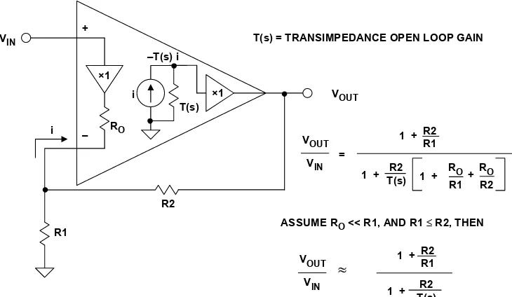
Current Feedback Amplifier Basics
The basic current feedback amplifier topology is shown in Figure 1-14 below. Notice that within the model, a unity gain buffer connects the non-inverting input to the inverting input. In the ideal case, the output impedance of this buffer is zero (RO = 0), and the error
signal is a small current, i, which flows into the inverting input. The error current, i, is mirrored into a high impedance, T(s), and the voltage developed across T(s) is equal to T(s)·i. (The quantity T(s) is generally referred to as the open-loop transimpedance gain.)
This voltage is then buffered, and is connected to the op amp output. If RO is assumed to
be zero, it is easy to derive the expression for the closed-loop gain, VOUT/VIN, in terms of
the R1-R2 feedback network and the open-loop transimpedance gain, T(s). The equation can also be derived quite easily for a finite RO, and Fig. 1-14 gives both expressions.
Figure 1-14: Current feedback (CFB) op amp topology
At this point it should be noted that current feedback op amps are often called
transimpedance op amps, because the open-loop transfer function is in fact an impedance as described above. However, the term transimpedance amplifier is often applied to more general circuits such as current-to-voltage (I/V) converters, where either CFB or VFB op amps can be used. Therefore, some caution is warranted when the term transimpedance is encountered in a given application. On the other hand, the term current feedback op amp
is rarely confused and is the preferred nomenclature when referring to op amp topology.
From this simple model, several important CFB op amp characteristics can be deduced.
• Unlike VFB op amps, CFB op amps do not have balanced inputs. Instead, the non-inverting input is high impedance, and the non-inverting input is low impedance.
• The open-loop gain of CFB op amps is measured in units of Ω (transimpedance gain) rather than V/V as for VFB op amps.
+
– i
–T(s) i
T(s) = TRANSIMPEDANCE OPEN LOOP GAIN
T(s) RO
i ×1
R2
R1 VIN
VOUT
VOUT
VIN
1 + R2 R1
1 + T(s)R2 1 + RO =
1 + R2 R1
1 + T(s)R2
≈
R1+ RO R2
ASSUME RO<< R1, AND R1 ≤R2, THEN
VOUT
• For a fixed value feedback resistor R2, the closed-loop gain of a CFB can be varied by changing R1, without significantly affecting the closed-loop bandwidth. This can be seen by examining the simplified equation in Fig. 1-14. The denominator
determines the overall frequency response; and if R2 is constant, then R1 of the numerator can be changed (thereby changing the gain) without affecting the denominator— hence the bandwidth remains relatively constant.
The CFB topology is primarily used where the ultimate in high speed and low distortion is required. The fundamental concept is based on the fact that in bipolar transistor circuits currents can be switched faster than voltages, all other things being equal. A more
detailed discussion of CFB op amp AC characteristics can be found in Section 1-5.
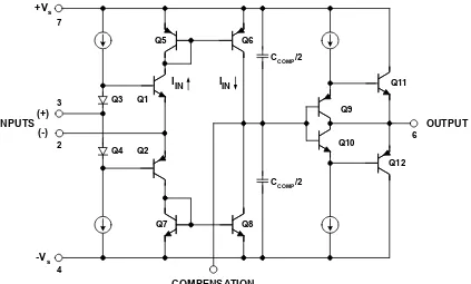
Figure 1-15 below shows a simplified schematic of an early IC CFB op amp, the AD846— introduced by Analog Devices in 1988 (see Reference 1). Notice that full advantage is taken of the complementary bipolar (CB) process which provides well matched high ft PNP and NPN transistors.
Figure 1-15: AD846 current feedback op amp (1988)
Transistors Q1-Q2 buffer the non-inverting input (pin 3) and drive the inverting input (pin 2). Q5-Q6 and Q7-Q8 act as current mirrors that drive the high impedance node. The CCOMP capacitor provides the dominant pole compensation; and Q9, Q10, Q11, and Q12
comprise the output buffer. In order to take full advantage of the CFB architecture, a high speed complementary bipolar (CB) IC process is required. With modern IC processes, this is readily achievable, allowing direct coupling in the signal path of the amplifier.
However, the basic concept of current feedback can be traced all the way back to early vacuum tube feedback circuitry, which used negative feedback to the input tube cathode. This use of the cathode for feedback would be analogous to the CFB op amp's low
CCOMP/2
COMPENSATION
Q6
Q8
+Vs
INPUTS
-Vs
Q1
Q2 Q5
Q7 Q3
Q4
4 3
2 7
CCOMP/2
OUTPUT
Q9
Q11
Q12 Q10
6
IIN
(+)
(-)
Current Feedback Using Vacuum Tubes
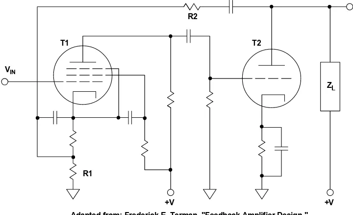
Figure 1-16 below is an adaptation from a 1937 article on feedback amplifiers by
Frederick E. Terman (see Reference 2). Notice that the AC-coupled R2 feedback resistor for this two-stage amplifier is connected to the low impedance cathode of T1, the pentode vacuum tube input stage. Similar examples of early tube circuits using cathode feedback can be found in Reference 3.
DC-coupled op amp design using vacuum tubes was difficult for numerous reasons. One reason was a lack of suitable level shifters. Multi-stage op amps either required extremely high supply voltages or suffered gain loss because of resistive level shifters. In a 1941 article, Stewart E. Miller describes how to use gas discharge tubes as level shifters in several vacuum tube amplifier circuits (see Reference 4). A circuit of particular interest is shown in Figure 1-17 (opposite).
Figure 1-16: A 1937 vacuum tube feedback circuit designed by
Frederick E. Terman, using current feedback to the low impedance input cathode (adapted from Reference 2)
In the Fig. 1-17 reproduction of Miller's circuit, the R2 feedback resistor and the R1 gain setting resistor are labeled for clarity, and it can be seen that feedback is to the low impedance cathode of the input tube. The author suggests that the closed-loop gain of the amplifier can be adjusted from 72dB-102dB, by varying the R1 gain-setting resistor from 37.4Ω to 1.04Ω.
What is really interesting about the Miller circuit is its frequency response, which is reproduced in Figure 1-18 (opposite). Notice that the closed-loop bandwidth is nearly independent of the gain setting, and the circuit certainly does not exhibit a constant gain-bandwidth product as would be expected for a traditional VFB op amp.
ZL
+V +V
VIN
R2
R1
T1 T2
For a gain of 72dB, the bandwidth is about 30kHz, and for a gain of 102dB (30dB
increase), the bandwidth only drops to ~15kHz. With a 72dB gain at 30kHz VFB op amp, bandwidth would be expected to drop 5 octaves to ~0.9kHz for 102dB of gain.
Figure 1-17: A 1941 vacuum tube feedback circuit using current feedback
To clarify this point on bandwidth, a standard VFB op amp 6dB/octave (20dB/decade) slope has been added to Fig. 1-18 for reference.
Figure 1-18: A 1941 feedback circuit shows characteristic CFB gain-bandwidth relationship
Although there is no mention of the significance of this within the text of the actual article, it nevertheless illustrates a popular application of CFB behavior, in the design of high speed programmable gain amplifiers with relatively constant bandwidth.
FEEDBACK RESISTOR (R2) (151kΩ)
GAIN (R1) 1.04Ω- 37.4Ω
Adapted from: Stewart E. Miller, "Sensitive DC Amplifier with AC Operation," Electronics, November 1941, pp. 27-31, 105-109
Adapted from: Stewart E. Miller, "Sensitive DC Amplifier with AC Operation," Electronics, November 1941, pp. 27-31, 105-109
When transistor circuits ultimately replaced vacuum tube circuits between the late 1950s and the mid-1960s, the current feedback architecture became popular for certain high speed op amps. Figure 1-19 below shows a fast-settling op amp designed at Bell Labs in 1965, for use as a building block in high speed A/D converters (see Reference 5).
The circuit shown is a composite amplifier containing a high speed AC amplifier (shown inside the dotted outline) and a separate DC servo amplifier loop (not shown). The feedback resistor R2 is AC coupled to the low-impedance emitter of transistor Q1. The circuit design was somewhat awkward because of the lack of good high frequency PNP transistors, and it also required zener diode level shifters, and non-standard supplies.
Figure 1-19: A 1965 solid state current feedback op amp design from Bell Labs
Hybrid circuit manufacturing technology, which was well established by the 1980s, allowed the use of fast, relatively well-matched NPN and PNP transistors, to realize CFB op amps. The Analog Devices' AD9610 and AD9611 hybrids were good examples of these devices introduced in the mid-1980s.
With the development of high speed complementary bipolar IC processes in the 1980s (see Reference 6) it became possible to realize completely DC-coupled current feedback op amps using PNP and NPN transistors such as the Analog Devices' AD846, introduced in 1988 (Fig. 1-15, again). Device matching and clever circuit design techniques give these modern IC CFB op amps excellent AC and DC performance without a requirement for separate level shifters, awkward supply voltages, or separate DC servo loops.
Various patents have been issued for these types of designs (see References 7 and 8, for example), but it should be remembered that the fundamental concepts were established decades earlier.
TO DC SERVO AMP R2
R1
Adapted from: J. O. Edson and H. H. Henning, "Broadband Codecs for an Experimental 224Mb/s PCM Terminal," BSTJ, Vol. 44, No. 9, November 1965, pp. 1887-1950
REFERENCES: OP AMP TOPOLOGIES
1. Wyn Palmer, Barry Hilton, "A 500V/µs 12 Bit Transimpedance Amplifier," ISSCC Digest, February 1987, pp. 176-177, 386.
2. Frederick E. Terman, "Feedback Amplifier Design," Electronics, January 1937, pp. 12-15, 50. 3. Edward L. Ginzton, "DC Amplifier Design Techniques," Electronics, March 1944, pp. 98-102. 4. Stewart E. Miller, "Sensitive DC Amplifier with AC Operation," Electronics, November 1941, pp.
27-31, 105-109.
5. J. O. Edson and H. H. Henning, "Broadband Codecs for an Experimental 224Mb/s PCM Terminal,"
Bell System Technical Journal, Vol. 44, No. 9, November 1965, pp. 1887-1950.
6. "Op Amps Combine Superb DC Precision and Fast Settling," Analog Dialogue, Vol. 22, No. 2, pp. 12-15.
7. David A. Nelson, "Settling Time Reduction in Wide-Band Direct-Coupled Transistor Amplifiers,"
US Patent 4,502,020, Filed October 26, 1983, Issued February 26, 1985.
SECTION 1-3: OP AMP STRUCTURES
Walt Kester, Walt Jung, James Bryant
This section describes op amps in terms of their structures, and Section 1-4 discusses op amp specifications. It is hard to decide which to discuss first, since discussion of
specifications, to be useful, entails reference to structures, and discussion of structures likewise requires reference to the performance feature that they are intended to optimize.
Since the majority of readers will have at least some familiarity with operational amplifiers and their specifications, we shall discuss structures first, and assume that readers will have at least a first-order idea of the definitions of the various specifications. Where this assumption proves ill-founded, the reader should look ahead to the next section to verify any definitions required.
Because single-supply devices permeate practically all modern system designs, the related design issues are integrated into the following op amp structural discussions.
Single-Supply Op Amp Issues
Over the last several years, single-supply operation has become an increasingly important requirement because of market demands. Automotive, set-top box, camera/cam-corder, PC, and laptop computer applications are demanding IC vendors to supply an array of linear devices that operate on a single-supply rail, with the same performance of dual supply parts. Power consumption is now a key parameter for line or battery operated systems, and in some instances, more important than cost. This makes low-voltage/low supply current operation critical; at the same time, however, accuracy and precision requirements have forced IC manufacturers to meet the challenge of "doing more with less" in their amplifier designs.
In a single-supply application, the most immediate effect on the performance of an amplifier is the reduced input and output signal range. As a result of these lower input and output signal excursions, amplifier circuits become more sensitive to internal and external error sources. Precision amplifier offset voltages on the order of 0.1mV are less than a 0.04 LSB error source in a 12-bit, 10V full-scale system. In a single-supply system, however, a "rail-to-rail" precision amplifier with an offset voltage of 1mV represents a 0.8LSB error in a 5V fullscale system (or 1.6LSB for 2.5V fullscale).
To keep battery current drain low, larger resistors are usually used around the op amp. Since the bias current flows through these larger resistors, they can generate offset errors equal to or greater than the amplifier's own offset voltage.
OP113/213/413 family, do have high open-loop gains (>120dB), for use in demanding applications. Another example would be the AD855x chopper-stabilized op amp series.
Many trade-offs are possible in the design of a single-supply amplifier circuit— speed versus power, noise versus power, precision versus speed and power, etc. Even if the noise floor remains constant (highly unlikely), the signal-to-noise ratio will drop as the signal amplitude decreases.
Besides these limitations, many other design considerations that are otherwise minor issues in dual-supply amplifiers now become important. For example, signal-to-noise (SNR) performance degrades as a result of reduced signal swing. "Ground reference" is no longer a simple choice, as one reference voltage may work for some devices, but not others. Amplifier voltage noise increases as operating supply current drops, and
bandwidth decreases. Achieving adequate bandwidth and required precision with a somewhat limited selection of amplifiers presents significant system design challenges in single-supply, low-power applications.
Most circuit designers take "ground" reference for granted. Many analog circuits scale their input and output ranges about a ground reference. In dual-supply applications, a reference that splits the supplies (0V) is very convenient, as there is equal supply headroom in each direction, and 0V is generally the voltage on the low impedance ground plane.
In single-supply/rail-to-rail circuits, however, the ground reference can be chosen
anywhere within the supply range of the circuit, since there is no standard to follow. The choice of ground reference depends on the type of signals processed and the amplifier characteristics. For example, choosing the negative rail as the ground reference may optimize the dynamic range of an op amp whose output is designed to swing to 0V. On the other hand, the signal may require level shifting in order to be compatible with the input of other devices (such as ADCs) that are not designed to operate at 0V input.
Very early single-supply "zero-in, zero-out" amplifiers were designed on bipolar
processes, which optimized the performance of the NPN transistors. The PNP transistors were either lateral or substrate PNPs with much less bandwidth than the NPNs. Fully complementary processes are now required for the new-breed of single-supply/rail-to-rail operational amplifiers. These new amplifier designs don't use lateral or substrate PNP transistors within the signal path, but incorporate parallel NPN and PNP input stages to accommodate input signal swings from ground to the positive supply rail. Furthermore, rail-to-rail output stages are designed with bipolar NPN and PNP common-emitter, or N-channel/P-channel common-source amplifiers whose collector-emitter saturation voltage or drain-source channel on-resistance determine output signal swing, as a function of the load current.
input common-mode voltage range from 0V to the positive supply are good candidates. It is not necessary that amplifiers maintain common-mode rejection for signals beyond the supply voltages. But, what is required is that they do not self-destruct for momentary overvoltage conditions! Furthermore, amplifiers that have offset voltages less than 1mV and offset voltage drifts less than 2µV/°C are also very good candidates for precision applications. Since input signal dynamic range and SNR are equally if not more important than output dynamic range and SNR, precision single-supply/rail-to-rail operational amplifiers should have noise levels referred-to-input (RTI) less than 5µVp-p in the 0.1Hz to 10Hz band.
The need for rail-to-rail amplifier output stages is also driven by the need to maintain wide dynamic range in low-supply voltage applications. A single-supply/rail-to-rail amplifier should have output voltage swings that are within at least 100mV of either supply rail (under a nominal load). The output voltage swing is very dependent on output stage topology and load current.
Figure 1-20: Single-supply op amp design issues
Generally, the voltage swing of a good rail-to-rail output stage should maintain its rated swing for loads down to 10kΩ. The smaller the VOL and the larger the VOH, the better.
System parameters, such as "zero-scale" or "full-scale" output voltage, should be determined by an amplifier's VOL (for zero-scale) and VOH (for full-scale).
Since the majority of single-supply data acquisition systems require at least 12- to 14-bit performance, amplifiers which exhibit an open-loop gain greater than 30,000 for all loading conditions are good choices in precision applications. Single-supply op amp design issues are summarized in Figure 1-20 above.
Single Supply Offers:
z Lower Power
z Battery Operated Portable Equipment
z Requires Only One Voltage
Design Tradeoffs:
z Reduced Signal Swing Increases Sensitivity to Errors Caused by Offset Voltage, Bias Current, Finite Open-Loop Gain, Noise, etc.
z Must Usually Share Noisy Digital Supply
z Rail-to-Rail Input and Output Needed to Increase Signal Swing
z Precision Less than the best Dual Supply Op Amps but not Required for All Applications