Sponsoredby:
BERCA
Ha rd a ya p e rka sa
B E Y O N D T E C H N O L O G Y Agilent TechnologiesRCS
RA DAR & COMMU NICATION SYS TEMSINFRA RCS
I N D O N E S I A
Organizeby:
LIPI
AsRI
ii
Microwave, Electronics And Telecommunications
(ICRAMET) 2012
“Developing Regional and International Scientific Cooperations
”
Editor
Mashury Wahab
Yadi Radiansah
Technical Editor
Hana Arisesa
Arief Nur Rahman
Taufiqqurrachman
Arief Budi santiko
Layout and Cover
Dicky Desmunandar
ISSN : 1979-2921
Published by :
Research Center for Electronics and
Telecommunication
Indonesian Institute of Sciences
Kampus LIPI Jl. Sangkuriang Bandung 40135
Phone : +62 22 2504660
Fax : +62 22 2504659
iii
Advisory Chair
Prof. Dr. Lukman Hakim, LIPI Chairman
Prof. Dr. Akhmaloka, ITB Rector
Prof. Dr. Leo P. Ligthart, IRCTR-I
Steering Committee
SyahrulAiman, LIPI
HiskiaSirait, LIPI
JosaphatTetuko S.S., Chiba Univ.
Raja SyamsulAzmir A., UPM Malaysia
EkoTjiptoRaharjo, UI
FitriYuli, UI
MashuryWahab, LIPI
YuyuWahyu, LIPI
GoibWiranto, LIPI
PurwokoAdhi, LIPI
Syamsu Ismail, LIPI
Arwin D.W. Sumari, AAU
Andriyan B. Suksmono, ITB
Nana Rachmana, ITB
AditKurniawan, ITB
SholehHadi P. , UNIBRAW
A. Andaya Lestari, IRCTR-I
EndonBharata, IRCTR-I
EdySiradjt, BalitbangKemhan
HammamRiza, BPPT
Technical Program Committee
Chairman
Dr. MashuryWahab
Vice Chairman
YadiRadiansah
Secretariat
Emil Kristanti, LIPI
Poppy Sumarni, LIPI
Lisdiani, LIPI
Finace Division
Zaenul Arifin
Program Division
iv
Novita Dwi Susanti, LIPI
Publication Division
Arief Nur Rahman, LIPI
Hana Arisesa, LIPI
Taufiqurrahman, LIPI
Arief Budi Santiko, LIPI
Dicky Desmunandar, LIPI
Documentation Division
Endang Ridwan, LIPI
Registration Division
Zaeunul Arifin
Emil Kristanti
Nani Haryati
Poppy Sumarni
Lisdiani
Poster Coordinator
Deni Permana K
Dadin Mahmudin
Equipment & Exhibition Division
Patricius Sriyono,LIPI
Aseni, LIPI
Dicky Desmunandar
Logistic Division
Anna Kristina Tampubolon
Nani Haryati
Asisten Presentation
v
On behalf of Chairman Organizing Committee of the 6
thNational Radar Seminar and
International Conference on
Radar, Antenna, Microwave, Electronic and
Telecommunications (ICRAMET) 2012, I would like to thank all the participants for
their participation during the 6
thNational Radar Seminar and the first International
Conference on Radar, Antenna, Microwave, Electronic and Telecommunications
(ICRAMET) 2012 that hold in Bali on April 23-24, 2012.
The 6
thNational Radar Seminar and the first International Conference on Radar,
Antenna, Microwave, Electronic and Telecommunications (ICRAMET) 2012 is an
annual event organized by Research Center for Electronics and Telecommunications
(PPET-LIPI), School of Electronics and Informatics (STEI-ITB), Indonesian Radar
Association (AsRI), International Research Centre for Telecommunications and
Radar-Indonesia (IRCTR-I), and IEEE MTT/AP-S Radar-Indonesian Chapter. This seminar is a
forum for socialization and discussion among researchers, observer, top scientists, and
users of Radar. It is expected that solutions, technologies, and policies in Radar can be
produced in this Seminar.
I would like to specifically express my gratitude to the chairman of Indonesian Institute
of Sciences (LIPI) Prof Dr. Lukman Hakim,Keynote speakers : Prof. Leo P. Ligthart of
TU Delft, Prof. R. Prasad from Aalborg University of Denmark, Dr. Atmaji Wisesa as a
representative of the Indonesian Industries and Kolonel Hetharia as the chief
commander of the Indonesian Airforce Radar Workshop .
This proceeding consists of 41 scientific papers. Some of these papers presented as oral
presentation, and the rest will be presented as poster presentation during the two-days
seminar on 23-24 April 2012. I truly hope that this seminar will be able to provide an
interesting session and serve as an excellent forum for a live technical discussion.
Last but not least, this seminar would not be possible without the contribution of the
Speakers, the Authors, the Advisory Committee, and the member of the Organizing
Committee.Therefore, I would like to take this opportunity to express my sincere
appreciation to all ofthem for execution of the the 6
thNational Radar Seminar and the
first International Conference on Radar, Antenna, Microwave, Electronic and
Telecommunications (ICRAMET) 2012.
Chairman OrganizingCommittee
vi
PREFACE ... v
CONTENTS... vi
1.
Simulation Design Indoor Antenna TV Gain High at Frequency 470 MHz -
890 MHz
... 01
2.
Bandwidth and Gain Enhancement of Aperture Coupled FedRectangular Patch
Antenna Using Hour-Glass Shaped Slot
... 06
3.
Comparison Study of One Unit Cell Electromagnetic Band Gapby Varying
The Patch Shape
... 14
4.
An Internally Connected Dye Solar Cell Module with Z-type SeriesConnection
... 15
5.
Design of RMS (Root Mean Square) Power DetectorAtFrequency of 2.4GHz
for WiMax System
... 20
6.
Visualization of RMS Power Measurement Results on RF System Using the
AVR Microcontroller AVR ATmega 8535
... 21
7.
VCO (Voltage Controlled Oscillator) Of Exciter Design For Electronic
Jammer Using IC MC 1648
... 22
8.
Upwelling Detection In North Moluccas Waters With MODIS SST And
Chlorophyll Data
... 27
9.
Correlation between material quality and performance in the multicrystalline
silicon solar cells
... 32
10.
TextureAnalysis
using
Autocorrelation
Feature
forMalariaParasitesin
Peripheral BloodImage
... 36
11.
Design of Film Thickness for Power Detector Application on C Band
Frequency
... 41
12.
Mercury Sensor using Surface Acoustic Wave Devices
... 44
13.
Applied Adaptive Neural Network Control of a Semi-ActiveSuspension
Systems Subjected to Road
... 45
14.
Nonlinear Principal Component Analysis Application for P300 Extraction and
Classification
... 49
15.
Visual Servoing Tracking Control Of A Ball And Plate System
... 53
16.
Design and Implementation Of Vision-Based Planar Juggler Control System
... 61
17.
Characteristic of daytime 150-km field-aligned irregularities observed with
Equatorial Atmosphere Radar at low latitude region in Indonesia
... 67
18.
Design and Simulation of 456 MHz Bandpass Filterwith for Radar System
... 68
19.
Proposal of Fiber-Remoted Radar Systems
... 73
20.
The Effect of Target Crossing Angle to the Forward Scattering Radar Spectra
... 77
21.
Study of Pulsed Doppler Radar Signal Processing (VHF Radar LAPAN
Implementation)
... 78
22.
The influence of different baseline lengths to ground targetsignature in a low
frequency Forward Scatter Micro-Radar
... 79
23.
Object Extraction Using Clustering For Surveillance Radar
... 80
24.
A Review Paper On Network Security For Surveillance Radar Network
... 84
25.
Radar Image Segmentation Using Fractal Dimension And Fuzzy Dynamic
Learning Neural Network
... 90
26.
Study Of FMCW Radar By Implementation USRP And GNU Radio
... 91
vii
for Ground Penetration Radar Appllication
... 107
31.
Radar Cross Section Calibration using trihedral reflektor for LIPI Coastal
Surveillance Radar
... 112
32.
Design and Simulation of 160 MHz Band Pass filter with 60 MHz Bandwidth
... 113
33.
Characteristic of L-Band EDFA for Fiber Optic Telecommunication Systems
... 117
34.
Development of a Remote Access System for Radar Network
... 118
35.
Design of High Power Amplifier System forDigital TelevisionTransmitter
DVB-T Standardusing LDMOS Devices Module
... 123
36.
Cross-correlation Optimization to Maintain MeasurementStability on Radio
Transmitter Azimuth Angle
... 128
37.
The Characteristics Of Uniform Fibre Bragg Gratings In The Two Layer Of
Refractive Index N1 And N2
... 133
38.
Multiband printed antenna design forCellular/Wimax application
... 138
39.
WiMAX Roaming Study for Broadband Wireless Communication in
Indonesia
... 144
40.
GOS Performance Comparison of an FCA And DCAChannel Assignment
Technique Of Urban MicrocellIn Manhattan Type Environment
... 145
41.
A Study on The Behaviour of M-type Strontium Hexagonal Ferrite Based
Microwave Absorbing
... 148
1
Simulation Design Indoor Antenna TV high Gain at
Frequency 470 MHz-890 MHz
Nasrulloh1, Surya Agam1, Sofian Hamid1
1Department of Electrical Engineering, Faculty of Science and Technology, University of Al Azhar indonesia,
Road Sisingamangaraja, Kebayoran Baru, Jakarta, 12110, phone (021) 727 92753, fax (021)-724-4767 Jakarta, Indonesia
Email : [email protected], [email protected]1, [email protected]1
Abstract—In this paper, the authors simulate the working area of the antenna for the frequencies used for TV applications is in the range 470 MHz - 890 MHz. Antenna which is designed indoor TV antenna which has the specifications above 8 dBi gain, has a large corner Half Power Beamwidth (HPBW) of more than 300, and work on the 75 ohm system. This meant that the antenna is able to work out is comparable to a standard TV antenna installed by
the community. With a literature review and simulation
methods, the authors use a variety of relevant data and simulate the antenna design to see radiation pattern, directivity, HPBW of the antenna design that has been made on software.
Keywords-component; indoor antenna TV , high gain, radiation pattern, HPBW
I. INTRODUCTION
Antenna as an element in the telecommunications needs of continuous innovation and creation, so the quality and benefits that can be felt bigger and more spacious feel. The antenna is one of the important elements that must exist in a radio telescope, television, radar, and all other communication tools that use the signal. An antenna is a vital part of a transmitter or receiver which is used to distribute radio signals in the air. Diverse forms of antenna in accordance with the design, deployment patterns, frequency and gain. Effective antenna length is the wavelength of the radio frequency it emits.
According to international regulations relating to setting the frequency of use (Radio Regulations) for television broadcasting in the VHF and UHF frequency bands. The history of television in Indonesia started in 1962 by TVRI in Jakarta using VHF television transmitters. Development transmitter TVRI running quickly, especially after the launch of satellites palapa in 1975. In 1987, the birth of the first private television station broadcasting in Indonesia, the transmitting station TVRI has reached at least 200 the number of stations which are all using VHF frequencies, and the first private TV transmitter is assigned a frequency allocation in the UHF band. Policy for use of the VHF frequency band and UHF TVRI to private. Interpretation so as to catch the TV antenna VHF and UHF are used that are designed and manufactured in accordance with the structure needed to get a
TV picture and sound quality is good and capable of generating a lot of channels.
II. THEORY
The antenna is a device that serves to transfer energy from the electromagnetic waves into the air or cable media reverse from the air to cable. Because it is the intermediary between the cable and the air, then the antenna must have the appropriate properties (match) with a successor cable media. This principle has been explained in the transmission line. In designing an antenna, a few things to note are:
- The shape and direction of the desired radiation - Polarization owned
- The working frequency, - lbandwidth
- Input impedance owned.
For an antenna that works on the band VLF, LF, HF, VHF and UHF down, type of antenna wire (antenna wire) is often used in practice, as well as 1/2λ dipole antenna, monopole antenna with ground plane, loop antennas, Yagi-Uda antenna array, the log periodic antenna and so on. Antennas of this type, physical dimensions adapted to the wavelength where the system works. The higher operating frequency, the shorter the wavelength, so the shorter the physical length of an antenna. In this paper all of simulation for design dan the result is using CST Microwave Studio software.
III. METHODS
2 IV. RESULT AND DISCUSSIONS
Based on a design that has been made, the antenna is able to produce high gain with a few other parameters included in the criteria of a good antenna is a Yagi-Uda antennas. This type of antenna has a directional pattern and is able to produce high gain because of its directors. indoor TV antenna with high gain is established by the CST program in accordance with the image below.
Figure 3.1 antenna design on the CST
From the picture design above, the type of antenna that designed is Yagi-Uda, a material used is PEC for the main part and the vacuum to the base. Yagi-Uda antenna is has three main parts, namely Reflector, Driven Element and Director. Reflector is the biggest part of the rear section having a length = 40 cm, width = 1.4 cm, and height = 14 cm. Driven Element is the part that will be connected to the port to be connected to the TV. Port on the image above the red in the middle of Driven Element with 75 ohm impedance. Driven element size in the design above is the length = 25 cm, width = 1.4 cm, height = 10 cm, and slit width = 1.8 cm gap. Director on the design on as many as 5 pieces, each having a size equal to the length = 22 cm, width = 1.45 cm, height = 7 cm, and slit width = 4 cm gap. The distance from the reflector to driven element is 12.05 cm. The distance from the driven element to the director one is 6 cm, and the distance between the director is 5.55 cm.
Figure 3.2 graphic S1, 1
S-Parameter Simulation results on the antenna design can be seen in the graph picture above. Value of S1,1 on the simulation result can be seen like above. Based on the picture, the value of S1, 1 in the frequency range between 470 MHz - 890 MHz has a value below -10 dB, so this result has been able to demonstrate that the design meets the criteria for the parameters S1, 1.
In addition to the value of S1,1, other parameter to consider is the value of the real and imaginary impedance. A good design will have a real impedance values range from about 75 ohms and the imaginary impedance range of approximately 0 ohms.
Figure 3.3 Real impedance value on the field Z
Real impedance values obtained in simulations is different over a range of 470 MHz - 890 MHz. Value near 75 ohms at a frequency of 470 MHz-760 MHz, while the frequencies between 750 MHz - 890 MHz have impedance ranges between 70-40 MHz.
3 Figure 3.4 The value on the imaginary impedance Z
Voltage Standing Wave Ratio (VSWR) as a parameter the antenna must have a value between 1-2. Design that will better demonstrate the value of VSWR is close to 1.
Figure 3.5 Graph of VSWR
VSWR value in the frequency range 470 MHz to 890 MHz are in the 1-2, so these results show that design has been created and simulated to meet the criteria for making the actual antenna.
To view the radiation pattern and direction of the antenna design and also know the size of the gain of the antenna directivity can be seen the results on farfield graphs in 3 dimensions and in the polar. To see the ability and the quality of the antenna design, it is necessary to view information on the farfield as the initial frequency of 500 Mhz. Farfield at a frequency of 650 MHz as a guide and Farfield intermediate frequency at a frequency of 800 MHz as reference frequency of the end for TV antenna applications.
Figure 3.6 3D farfield for a frequency of 500 MHz
Gain at a frequency of 500 MHz is 8.03 dBi, this means a minimum antenna gain has been met. In the polar theta and phi are known Half Power Beamwidth of the antenna has a wide angle 780 in the direction of theta and phi of 97.90 at. This shows the wide angle range is quite large.
Figure 3.7 farfield polar theta at 500 MHz
4 Figure 3.8 farfield polar phi at 500 MHz
From figure, we know that it have angular width (3 dB) about 97.9 degree, it means that at frequency about 500 MHz, the antenna has quite large angle to cover the area.
Figure 3.9 3D farfield frequency to 650 MHz
Gain at 650 MHz frequency is 9.47 dBi, this value is quite large compared to the gain at a frequency f = 500 MHz.
Figure 3.10 farfield polar theta at 650 MHz
In the polar direction theta is known Half Power Beamwidth antenna has a wide angle of 69.80. Great coverage
of this angle is more narrow than the frequency of 500 MHz
Figure 3.11 farfield polar phi at 650 MHz
While the Half Power Beamwidth of the antenna has a wide angle of 104.20 on phi. This shows the wide range of angles greater than the width of the coverage angle at a frequency of 500 MHz.
Figure 3.12 3D farfield to 800 MHz
5 Figure 3.13 farfield polar theta at 800 MHz
In the polar direction theta is known Half Power Beamwidth antenna has a wide angle of 69.80. Great coverage
of this angle is more narrow than the frequency of 500 MHz, but similar to the frequency of 650 MHz
Figure 3.14 farfield polar phi at 800 MHz
While the Half Power Beamwidth of the antenna has a wide angle of 300 on the phi polar directivity. This shows the wide
range of angles that are narrower than the width of the frequency range of angles at 500 MHz and 650 MHz.
V. CONCLUSION
Indoor antenna TV high gain that have frequency about 470 MHz-890 MHz from design above have good qualification. We can see from the value for each frequency we put to the simulation. About 3 example frequency, that is 500 MHz, 650 MHz, and 800 Mhz, all of frequency have gain >8 dBi, radiation pattern >300, S11 below -10dB in all
frequency we need, real impedance about 75 ohm, Imaginary impedansi about 0 ohm and the and the VSWR in range 1-2. From the simulation results is performed, antenna design for indoor applications to indoor TV antenna high gain character with some other parameters, this design can be used as a reference because it has met the aspects required to obtain a good quality antenna.
REFERENCES
[1] Boyle, Kevin, Zi Huang, Antennas From Theory to Practise, Wiley, New York : 2008
[2] Joel R. Hallas, Basic Antennas: Understanding Practical Antennas and Design, 2009.
[3] Constantine A. Balanis, Antenna Theory: Analysis and Design, 3rd Edition, John Wiley & Sons, 2005.
[4] Simon Haykin, Communications Systems 4th edition, John Wiley & Sons, 2001.
[5] J.-H. Lu, "Broadband dual-Frequency operation of circular patch antennas and arrays with a pair of L-shaped slots," IEEE Trans. Antennas Propagat., vol. 51, no. 5, pp. 1018-1023, May 2003.
Coupled Fed Rectangular Patch Antenna Using
Hour-Glass Shaped Slot With Back Cavity Dielectric
Taufal Hidayat1, Fitri Yuli Zulkifli2, Basari3, Eko Tjipto Rahardjo4
1,2,3,4 Antenna Propagation and Microwave Research Group (AMRG)
Department of Electrical Engineering, Faculty of Engineering, Universitas Indonesia Kampus Baru UI Depok, Indonesia
Tel: 021-7270078, Fax: 021-7270077
Email: [email protected], [email protected], [email protected], [email protected]
Abstract — In this paper, a single element aperture coupled rectangular patch is designed for future radar application, where its high gain and wide bandwidth is required. An aperture-coupled fed antenna is used to enhance the antenna’s gain and bandwidth. The antenna has a slot with glass shape. By adding the hour-glass shaped slot, the bandwidth of the antenna can be improved from 5% to 10%. The gain of the antenna can be achieved to 11.21 dBi when it is added with a back cavity dielectric in the middle of the structure. The antenna works from 2.80 – 3.10 GHz, where this band is a specification band for military radar application in Indonesia. The dimension of the antenna is 100mm x 100 mm by using Duroid 5880 substrate with dielectric constant 2.20 and total height of 1.524 mm.
Keywords — Aperture coupled microstrip antenna, bandwidth enhancement, high gain, hour-glass shape slot, back cavity dielectric
I. INTRODUCTION
Most of radar applications need high gain antenna for their system. Many high gain radar applications have relied upon parabolic reflectors [1]. However, such an antenna has important drawbacks especially for its bulky and heavy weight and its difficulty for fabrication as well. In order to mitigate the disadvantages of these drawbacks, the microstrip technology can be the solution. This is mostly due to their versatile in terms of possible geometries that makes them applicable for many different situations. The microstrip antenna has a lightweight construction and it is suitable for integration with microwave integrated circuits and other numerous advantages [2].
However, the microstrip antenna has also several drawbacks, especially the ability to achieve high gain and wide bandwidth. To solve these drawbacks, some techniques can be used for bandwidth broadening. One of the most common techniques is by using an aperture coupled fed patch antenna. The common aperture coupled feeding technique usually has 3−5 % bandwidth. Some papers have
shown that the aperture coupled feed with stacked patch can achieve the impedance bandwidth by 50−70% [3], [4]. However, the barrier of such antennas is poor from the front to back ratio and the back radiation. In order to solve this problem, the aperture coupled slot antenna can be combined with a cavity back configuration [5]. An appropriate size of the cavity can make the aperture has enough coupling to the patch, which makes the aperture and patch resonate mutually. Besides that, the back cavity will enhance the gain of the antenna, because the antenna radiation will be directed to the patch, instead of the back of antenna.
In order to improve the coupling in the aperture slot, some variation in geometry has been suggested. In this paper, variation in slot’s shape is designed for its aperture in the middle of antenna construction. There are several shape types of slots that can be used, such as “dog-bone”, bow-tie, or H-shaped [6]−[8]. The shape variation of the aperture slot has a significant impact on the strength of coupling between the feed line at lower layer and the patch at the upper layer [9]. Good coupling can affect the bandwidth of the antenna. This paper will design an hour glass shaped slot for the aperture coupled fed rectangular patch antenna. The hour glass shaped slot combines the advantages of H-shaped and “bowtie” shape slot. The sharp discontinues have been removed in “hour glass” shaped aperture allowing the field distribution inside the aperture to be more uniform. Therefore, a strong coupling can be achieved.
II. APERTURE COUPLED MICROSTRIP ANTENNA
The aperture coupled microstrip antenna employs a non contacting feeding technique, with either two parallel substrates, or two perpendicular techniques [2]. A strip line or microstrip feed line on one substrate is coupled through a small aperture in the ground plane that separates the two substrates to the microstrip patch element on the second substrate. A conventional geometry of the basic aperture coupled microstrip antenna is shown in Fig. 1 [10].
07 substrate. The thickness and dielectric constant of these to
substrates may thus be chosen independently to optimize the distinct electrical function of radiation and circuity. In designing the aperture coupled microstrip antenna, many variation of parameters influences the design, such as antenna’s substrate dielectric constant, antenna’s substrate thickness, microstrip patch length, microstrip antenna length, microstip antenna width, feed substrate dielectric constant, slot length, slot width, feed line width, feed line position relative to the slot, length of the stub, etc.
Figure 1. Geometry of aperture coupled antenna [10].
The aperture coupled microstrip can be modified to evolve the requirement parameters. One of the modification that can be done is the slot shape. The shape of the coupling aperture has a significant impact on the strenght of coupling between the feed line and the patch. Thin rectangular coupling slots have been used in the majority of aperture coupled microstrip antenna, as this gives better coupling than the rounded aperture.
The size of the patch of the antenna can be calculated by using equation (1) to (4) as follows [11]:
(1)
(2)
(3)
(4)
(a) Bird-eye view
(b) Side view
Figure 2. The proposed antenna structure (a) bird-eye view (b) side view
One of the useful features of the aperture coupled microstrip antenna is that it can provide substantially improved impedance bandwidth. While single layer probe fed element has limited impedance bandwidth of 2−5%, an aperture coupled element with modified slot is able to increase the impedance bandwidth [4]. This bandwidth improvement is primarily a result of the additional degrees of freedom that is offered by the feed line’s length and strong coupling from the aperture slot, which it depends on its size. The tuning feed line’s length can be adjusted by an offset of the inductive shift on the impedance Smith chart, which it generally occurs when a thick antenna substrate is used. Then, the aperture slot can be closely brought to the resonance frequency allowing a double tuning effect.
III. ANTENNA DESIGN
A. Element Configuration
08
Design of the patch element
The rectangular patch is used for the patch element, since it is the simplest configuration. The patch geometry is calculated using the equations (1)−(4). The rectangular patch has a radiating edge L and a non-radiating edge W as shown in Fig. 3. A commercially available CST Microwave Studio
has been used to numerically analyze a single element with a proper boundary condition. Using the equations (1) to (4), the calculation result yields L by 38.90 mm and W by 39.50 mm. The detail of the antenna structure is described in Fig. 3.
Design of the feed line
The radiating patch is fed by a 50 microstrip line. The width of the feed line is calculated using a transmission line calculator. As for 50 impedance microstrip line, the width of line is obtained by 1.5785 mm.
Design of the aperture slot
The slot dimension determines the amount of coupling to the patch from the feed line and the resonant frequency as well. The antenna is designed using an hour glass shaped slot, as previously mentioned in Introduction. The main parameter that influences the coupling level from the feed line to the patch is ratio between the outer width of the slot and the inner width the slot, noticed by a/b ratio in Fig. 3. Optimum coupling will yield the larger impedance bandwidth. The simulation result shows that when the a/b
ratio is 3, the electromagnetic energy is optimally coupled to the patch.
Figure 3. Geometry of hour-glass shaped slot.
Design of the stub length
The stub length refers to the length from the tip of the feed line to the position of the slot. The stub length will influence the impedance of the antenna. As for practical experiences, the stub length should be close to λg/4, and then the optimization for good impedance matching is started from this point.
B. Parametric Study
In this section, some main geometric parameters of this design, include patch size, slot size, geometry, and stub length will be studied. All of these parameters will influence the performance of the antenna.
of the patch to achieve resonant frequency at 3 GHz. In order to achieve a matching condition of the antenna, two main parameters should be considered, those are the aperture slot size and the feed length. The coupling level is primarily determined by the length of the coupling slot. The slot should therefore be made no longer than is required for impedance matching. Besides that, the outer-slot width (a) also affects the coupling level, but this does not affect too much compared to the stub length affect.
The two aforementioned parameters are carefully set so that the coupling is maximum from the feed to the patch through the aperture slot. The width of feed line is fixedly set by 1.59 mm. Length of the stub line changes the reactance of the slot aperture. The stub line is slightly less than λg/4 in length, shortening the stub line will move the locus in the capacitive direction on the Smith Chart. The length of feed line after adjusting the stub length is obtained by 3 cm to obtain the optimum value of the return loss characteristics.
As for bandwidth enhancement aiming at military radar application at the frequency 2.80 – 3.10 GHz, ratio between the outer-slot width (a) and the inner-slot width (b) as depicted in Fig. 3. This ratio is carefully arranged so that resulting the maximum coupling from the feed to the patch. From this characterization, optimum bandwidth enhancement can be obtained as the a/b ratio is set by 3. The a/b = 1 means that the slot is rectangular shape. The bandwidth optimization is shown in Fig. 4.
Figure 4. Characteristics of bandwidth performance according to the value of a/b ratio.
IV. SIMULATION RESULTS
09 of reflection coefficient (S11)is -33.50 dB. The impedance
bandwidth is achieved by approximately 10% from 2.80– 3.10 GHz for VSWR < 2. By this result, the target bandwidth has been satisfied with the target for aerial surveillance radar aimed at military purpose.
Figure 5. Reflection Coefficient of the antenna
The simulated radiation pattern and gain of the antenna without a back cavity is shown in Fig. 6 for 3D plot. It is shown that the back radiation still appears in the back of the antenna (180º of theta), allowing the total gain can be obtained only by 4.53 dBi.
Figure 6. Radiation pattern of the antenna without back cavity dielectric in 3D
This paper has proposed a back cavity dielectric configuration to increase the gain as described in the previous section and clearly depicted in Fig. 2. By this configuration, the simulation result shows that the total gain can be achieved by 11.90 dB in the center frequency 3 GHz at the elevation angle 90º as shown in Fig. 7. It means the gain is approximately improved by 7.37 dB (160%), which is very significant factor. Moreover, the absolute gain of the antenna is clarified by 11.21 dBi.
Figure 7. Radiation pattern of the antenna with back cavity dielectric in 3D
The cartesian plot is depicted in Fig. 8, which is shown a symmetrical beam pattern. The antenna beam is broadside direction beam with the 3-dB beamwidth is 61º. In addition, the first side lobe level (FSLL) is achieved at -21.50 dB below the main lobe peak magnitude.
Figure 8. Radiation pattern in cartesian plot along the theta.
V. CONCLUSION
A single element aperture coupled rectangular patch has been designed for future military aerial radar application in Indonesia. An aperture-coupled fed antenna is used to enhance the antenna bandwidth and gain as well, which is applied by employing a hour-glass slot for enhancing the bandwidth and a back cavity dielectric for increasing the gain. The simulated S-parameter meets the
10
[2] D.M. Pozar and R.W. Jackson, “An aperture coupled microstrip antenna with a proximity feed on a perpendicular substrate,” IEEE Trans. Antennas Propag., AP-35, pp. 728−731, June 1987.
[3] S.D. Targonski, R.B. Waterhouse, and D.M. Pozar, “Wideband aperture coupled stacked patch using thick substrates,” Electron. Lett., vol.32, no.21, pp. 1941−1942, Oct. 1996.
[4] S.D. Targonski, R.B. Waterhouse, and D.M. Pozar, "Design of wideband aperture-stacked patch microstrip antennas,” IEEE Trans. Antennas Propagat., vol. 46, no. 9, pp. 1245−1251, Sep. 1998. [5] D. Sun, W. Dou, and L. You, “A wide band aperture coupled
microstrip pacth antenna with back cavity of dielectric,” IEEE Trans Antennas Propagat, 2010.
[6] R.C. Hall and J.R. Sanford, “Performance enhancement for aperture coupled microstrip antenna,” in IEEE Antennas Propagat. Symp. Dig.,vol. 2, pp. 1040−1043, July 1992.
[7] M.E. Yazdi, M. Himdi, and J.P. Daniel, “Transmission line analysis of nonlinear slot coupled microstrip antenna,” Electron. Lett., vol. 28, no. 15, pp. 1406−1408, July 1992.
[8] X.H. Yang and L. Shafai, “Characteristics of aperture coupled microstrip antennas with various radiating patches and coupling apertures,” IEEE Trans. Antennas Propagat., vol. 43, pp. 72−78, Jan. 1995.
[9] V. Rathi, “Improved coupling for aperture coupled microstrip antennas,” IEEE Trans. Antennas Propag., vol. 44, no. 8, pp. 1196−1198, Aug. 1996.
[10] D.M. Pozar, “A review of aperture coupled microstrip antennas: history, operation, development, and applications,” University of Massachusetts, 1996.
11
Band Gap by Varying The Patch Shape
Fitri Yuli Zulkifli1 , Muhammad Idham Habibie2 and Eko Tjipto Rahardjo3
1,2,3 Antenna, Propagation and Microwave Research Group (AMRG)
Department of Electrical Engineering, Faculty of Engineering, Universitas Indonesia Kampus Baru UI, Depok, Indonesia
Email : [email protected], [email protected], [email protected]
Abstract—This paper conducts a comparison study of one unit cell electromagnetic bandgap (EBG). The reflection phase and reflection coefficient are the parameters observed in this study for each one unit EBG cell. Five different patch shapes as one unit cell EBG are observed in this paper. Simulation results show that the unit cell with hexagonal patch shape shows the best impedance matching compared to the other four unit cell shapes. While from reflection phase, the square shape shows resonance frequency at 9.4 GHz. The bandgap of the unit cells varies from 130 MHz up to 1090 MHz.
Keywords-component; electromagnetic bandgap, unit cell, reflection phase, reflection coefficient
I. INTRODUCTION
In the radar technology, antenna is known as one of the crucial component for Radar. Several antennas used for Radar application is including the waveguide slot antenna [1]-[4]. However the waveguide slot antenna array has a very large conducting plane, therefore the surface current can form standing wave and contribute to back radiation [4]. These effects will degrade the performance of the waveguide slot antenna array.
One method to solve this problem is using Electromagnetic Band Gap (EBG) structure. EBG structure is defined in [5] as “artificial periodic (or sometimes non-periodic) objects that prevent/assist the propagation of electromagnetic waves in a specified band of frequency for all incident angles and all polarization states”. Using EBG structure, it can suppress the surface wave in the antenna ground plane and increase the gain of the antenna. This is an important antenna performance for radar application because most radar applications requires high gain antenna. Several researches have used different EBG shapes like embedding mettalo-EBG structure in [6], fork-like EBG [7] and spiral shape EBG in [8].
In this paper, a comparison study of different basic shapes of one unit cell EBG is conducted. The parameters used in this study of the different shapes of one unit cell EBG are reflection phase and reflection coefficient. This EBG structure will be used as Artificial Magnetic Conductors (AMC) reflector to replace the conventional plane reflector.
II. ELECTROMAGNETIC BANDGAP
To analyze the EBG characteristics, various methods have been implemented. One of the methods for analyzing the EBG characteristics is the lumped element model. The EBG could be explained by using the lumped element model which consists of inductance L and capacitance C. These components could determine the frequency resonance and the reflection phase of the EBG. Figure 1 shows the Lumped inductance and capacitance for EBG analysis.
Figure 1. Lumped LC model for EBG analysis [5]
There are several methods for EBG, namely:
a. Double negative (DNG) materials with both negative permittivity and permeability.
b. Left-handed materials inside the electric, magnetic, and propagation direction satisfy a left-handed relation. c. Negative refractive index materials that have a
refractive index.
d. Magneto materials with artificially controlled high permeability.
e. High impedance surfaces with relatively large surface impedance for both TE and TM waves.
f. Artificial magnetic conductors (AMC) that exhibit the same properties as a perfect magnetic conductors.
For a high impedance surface or also called artificial magnetic conductor (AMC), the electric field has an antinode at the surface while the magnetic field has a node [9]. For this condition, the reflection phase can be determined as in Eq.1. For a normally incident wave, the reflection phase of the metamaterial-based AMC surface is given as :
12 (2)
Figure 2 shows the reflection phase for EBG. The phase is zero at the resonance frequency. The bandgap occurs between the phase π/2 and -π/2.
Figure 2. Reflection phase for EBG [9]
The reflection coefficient is another parameter observed in this paper. It describes how much energy is reflected after the waves suddenly crash due to the changes of mediums. Reflection coefficient has a magnitude from 0 to 1. In the graph depicted in Fig. 3, the reflection coefficient shows the logarithmic value so that the coefficient reflection has a magnitude from 0 to -∞ dB. This parameter can determine the
impedance bandwidth of antennas. In this figure, the red line shows the the impedance bandwidth is taken from coefficient reflection < -10 dB which is equivalent with VSWR < 2. Therefore the impedance bandwidth is from 1 GHz to 1.4 GHz, which is equal to 400 MHz bandwidth.
Figure 3. Impedance Bandwidth based on Reflection Coefficient
In this paper, five different unit cell shapes are designed and observed. The unit cell is designed to work at center frequency 9.4 GHz. All of the designs use the substrate FR-4 that is made of copper with
ε
r =4.3. The simulation uses CST Microwavestudio suite software.
A. Design 1
The first design uses the square shape patch with length of 5.85 mm as shown in Figure 4. To obtain the optimal design to the required frequency resonance, the size of the rectangular patch EBG is determined as follows:
Patch : 34.22 mm2 Ground plane : 69.72 mm2
Figure4. Design of the EBG square patch
B. Design 2
The second design is the circular patch as shown in Fig. 5. To get the optimal design of the required frequency resonance, the radius of the circular patch is 3.71 mm.
Figure 5. Design of the EBG circular patch
C. Design 3
13
Figure 6. Design of the EBG square ring slot
D. Design 4
The fourth design has the shape of equilateral triangle patch. To get the required resonance at 9.4 GHz, the design shows that the equilateral triangle has side length of 9.86 mm with bottom side length of 8.1 mm as depicted in Fig. 7.
Figure 7. Design of the EBG triangle patch
E. Design 5
The last design uses a hexagonal patch shape EBG unit cell. The radius of the patch in this design is 7.92 mm. Figure 8 shows the EBG design using hexagonal patch.
Figure 8. Design of the EBG Hexagonal Patch
IV. SIMULATION RESULTS
The parameters reflection coefficient and reflection phase of each unit cell EBG design has been simulated and observed. The simulation results are shown in Fig. 9 and Fig. 10.
Figure 9 shows the comparison of the five different EBG unit cell shapes based on the parameter reflection coefficient.
coefficient of -43.70 dB.
-50
Figure 9. Reflection coefficient for all unit cell EBG
Table 1 shows the detailed data of each EBG unit cell. The impedance bandwidth based on reflection coefficient < -10 dB shows that the unit cell has bandwidth from 200 MHz to 460MHz (however for square shape EBG unit cell has best impedance matching of -1.73 dB).
Table 1. Comparison of reflection coefficient
EBG unit cell
Square ring slot 9.30-9.50= 200
MHz -11,84
14
square ring slot circular square hexagonal triangular
Figure 9. Reflection Phase for all unit cell EBG
Table 2. Comparison of reflection phase
EBG unit cell
Five different unit cell EBG shapes are designed and simulated. Simulation result shows from the coefficient reflection that the hexagonal shape has the best impedance matching of -43.70 dB. The square shape however shows precisely 9.4 GHz frequency resonance based on reflection phase. Moreover, the
A
This paper is partially supported by research grant “Riset Utama Universitas Indonesia” with the contract number: 1606/H2.R12/HKP.05.00/2012.
REFERENCES
[1] Guaxin Fan and Jian-Ming Jin, “Scattering from a cylindrically conformal slotted-waveguide array antenna”, International Symposium on Antennas & Propagation Society Digest 1996, pp. 1394-1397
[2] Fitri Yuli Zulkifli, Ulil Ulya and Eko Tjipto Rahardjo, “Pengembangan Antena Waveguide 8 slot untuk Aplikasi Radar Pengawas Pantai”, Jurnal Elektronika dan Telekomunikasi, vol. 12, no.1, edisi Januari-Juni 2012
[3] Kazuhisa Sano and Kazuhiro Ito, “Dielectric Waveguide Slot Antenna with Integrated Filter For Automative UWB Radar Applications”, IEEE MTT-S International Microwave Symposium Digest 2008, pp. 113-116
[4] Lon Li, Xiao-Ji Dang, and Chang-Hong Liang, “Analysis and Design of Waveguide Slot Antenna Array Integrated With Electromagnetic Band-Gap Structures” IEEE Antennas and Wireless Propagation Letters, vol 5, 2006, pp.111-115
[5] Fan Yang, and Yahya Rahmat-Samii, Electromagnetic Bandgap Structures in Antena Engineering.Cambridge: The Cambridge RF and Microwave Engineering Series, Cambridge University Press, Book 2009
[6] D.N, Elsheakh, H.A, Elsadek, E.A, Abdallah, H.Elhenawy and M.F.Iskandar, “Enhancement of Microstrip Monopole Antenna Bandwidth by using EBG structure”, IEEE Antennas & Wireless Prop Letters, vol 8 2009, pp 959-962
[7] Li Yang, Zhenghe Feng, Fanghu Chen and Mingyan Fan, “ A Novel Compact Electromagnetic Band-Gap (EBG) Structure & its Application in Microstrip Antenna Arrays. IMTS 2004, vol.3, pp 1635-1638
[8] Li Yang, Mingyan Fan, and Zhenghe Feng, “Spiral EBG Structure and it’s application in microstrip and array”, Asia Pacific Microwave Conference (APMC) 2005, Vol 3
16 material for the scaling up of DSC module, which also shows a
good thermal stability on the range of -40 to 80oC.
According to Tulloch et al. [8], an integrated series connection for DSC module can be designed in 3 ways:
• Z-connection • W-connection • Monolithic connection
Figure 2 shows the cross-section design of the above connections. Further description with respect to the design and fabrication of those connections could be found in Refs [7, 8].
a).
b).
c).
Figure 2. Cross section structure of : a). Z-type b). W-type c). Monolithic connection for DSC [7].
In this work, we present in detail a design followed by fabrication of a DSC solar module with a Z-type integrated series connection. The reason for choosing Z-type connection is due to the effectiveness and simplicity of the printing method for each electrode. Unlike the W-type, the preparation of photoelectrode (TiO2 and dye -coated) and counter-electrode
(Pt-coated) are prepared on separate substrates. Moreover, in Z-connection, silver finger is employed to enhance the current collection (see Fig. 2 for more detail and comparison). Screen printing was used in our work to fabricate the cells as well as the barrier and interconnection. This technology allows easier and precise positioning of all layers.
II. EXPERIMENTAL
A. Design and Fabrication of Counter-Electrode
Figure 3 shows the design of counter-electrode. In this experiment, we designed DSC modules which consist of two cells. Each module was fabricated on 15Ω/□ transparent conducting oxide (TCO) glass with a size of 30x50 mm2.
a. b.
Figure 3. Top-view designs of two consecutive step in counter-electrode fabrication: a. laser scribing b. Pt printing.
The fabrication of counter-electrode was performed on 2 consecutive steps, i.e.: laser scribing and Pt printing. Laser scribing was done to remove the conducting TCO layer on the substrate. In Z-type connection, this step is particularly aimed to separate one cell to another (see Fig. 2.a). Glass frit layer will be deposited later on the TCO free area as a further barrier. Therefore, it is essential to make sure that the TCO layer has been fully scribed after each laser cutting process was performed.
The material we used as counter-electrode for each cell was platinum (Pt) catalyst paste which was deposited on fluorine tin oxide doped glass. The Pt paste was purchased from Dyesol, Australia and applied on the substrates using screen printing method. The printing process was performed on a synthetic nylon 200 mesh screen on an area of 9x48 mm2 for each cell
(see Fig. 3). This process was followed by a firing at a temperature of 450oC for approximately 15 minutes, resulting
17 Figure 4. Transparent Pt-coated counter-electrode.
B. Design and Fabrication of Photolectrode
The porous semiconductor of choice in this work was titanium dioxide (TiO2). TiO2 deposition was performed using
screen-printing technique which is relatively easy, low-cost, and industrially feasible. Similar to that of the counter-electrode preparation, the TiO2 printing was preceded by TCO
removal through laser scribing (see Fig.3.a. for the laser pattern). The printing area and the screen used to deposit the TiO2 layer were the same as the printing specifications for Pt
counter-electrode (Fig. 3.b).
The TiO2 pastes used in this experiment was Dyesol
18NR-T with a transparent sintered layer. 18NR-The printing process was performed twice, whereas each step was ended with a drying on an oven at a temperature of 175oC for 10 minutes. At the end of the process, all samples were sintered on a conveyor-belt furnace for 15 minutes. All samples were subsequently immersed on a solution consisting ruthenium dye Z907 and ethanol with a concentration of 20 mg/100 ml. The dyeing process lasted for 24 hours on a dark place and, in the end of the process; all samples were rinsed on ethanol. We suggested that the coloring time might be decreased by using higher concentrations of dye solution.
a. b.
Figure 3. Top-view designs of two consecutive step in counter-electrode fabrication: a. laser scribing; b. TiO2 printing.
C. Module Assembly
The assembly of the module was basically a process when counter-electrode and photoelectrode were sandwiched together to form complete cells. In a single cell, the incorporation normally involves thermoplastic sealing materials such as Surlyn or Bynel. In DSC module assembly, however, such method is somewhat difficult to perform
especially when it comes to a wide area module with complicated pattern. Therefore, printable materials such as hermetic sealing compound (glass frit) and silver paste are widely preferred as the sealing and conducting components.
The assembly process of our cells was performed as follows: first, glass frit was printed on the counter-electrode side according to the pattern shown in Fig. 4.a. The printing was performed twice, whereas the second printing was done 30 minutes in room temperature after the first deposition to allow the first glass frit layer to dry. The width of the as deposited glass frit layer was set to 0.7 mm. As the second step, Dupont silver paste with a width of 0.5 mm was printed on the photoelectrode side following the pattern shown in Figure 4.b. Both electrodes were subsequently attached together, in which the Pt layer was aligned on top of the TiO2.
This step needs to be done in a high precision manner as inaccuracies might result in short connection between the neighboring cells. Figure 4.c. shows the top-view pattern of the assembled module. The sandwiched module was subsequently clamped with a paper clip and set aside in room temperature to strengthen the bond.
a. b.
c.
Figure 4. Top-view design of: a. glass print pattern on counter-electrode; b. silver paste pattern on photoelectrode; c. final pattern after both electrodes
were sandwiched.
18 As the last step in cell assembly, liquid electrolyte was
injected through the air gap in each cell. The electrolyte used in this work was an iodide based electrolyte EL-HSE from Dyesol. Finally, the air gap was sealed using glass frit to prevent the electrolyte from being evaporated.
III. RESULTS AND DISCUSSION
Figure 5 shows a picture of the finished DSC modules, whereas each module contains two active dye solar cells. The overall appearance of each module is transparent with a total active area of 8.64 cm2 (or 2x4.32 cm2). Meanwhile, the current-voltage (I-V) characteristics data of our modules are provided in Table I and II. The measurements were performed under monochromatic lamp with an intensity of 7 mW/cm2.
Figure 5. DSC module containing 2 active cells.
Figure 6 shows the typical I-V curve of DSC module from the I-V measurement. We also provide two kinds of data, i.e. as-measured data and data measured 12 days after the fabrication (see Table I and II respectively). The overall results of this measurement indicate that the photoconversion efficieny of the fabricated modules are relatively low. It is suspected that the TiO2 thickness was not optimized enough for dye
absorption, hence, rendering the ability to absorb more photon. From both tables it can also be discerned that the repeatability of the photovoltaic output characteristics are relatively low. This is shown by large discrepancies across the devices. Further, the overall photo-conversion efficiency of module A is more than a factor of two higher compared to that of the module B. In order to reveal the reason for this, further analysis upon each electrical parameter is necessary. As an overall comparison between table 1 and table 2, it can be seen that the performance of both modules were relatively stable (or even better in some cases) after being stored for 12 days.
TABLE I. I-V CHARACTERISTICS DATA OF DSC MODULES WHICH WERE IMMEDIATELY MEASURED AFTER SEALED-OFF (ILLUMINATION INTENSITY 7 mW/cm2,R=1
DAYS AFTER FABRICATION (ILLUMINATION INTENSITY 7mW/cm2,R=1
Ω-82 modules shows more significant difference compared to the short circuit parameter. In a series connection, the final voltage is essentially the sum of the voltages produced by each cell at equal current. This can be explained through diode series connected circuit shown in Figure 7 which replicates the current flow (shown by the red dashed-arrow) in our series connected DSC modules. Meanwhile, currents are the same through all cells connected in series. The lower open circuit value shown by module B is therefore presumed to be rendered by lower characteristic exhibited by one of the cell. However, it is difficult to prove this probability as it is not possible to measure each cell individually in an internally connected DSC module. Based in our experiments on single DSC cell with 6 cm2 active area [jurnal TI], the open circuit voltage produced by each cell was normally around 0.5 V. This means for our module which consists of two cells, the open circuit voltage should ideally in the range of 0.9-1 V as VOC does not strongly
related to the wide of active area. This indicates that the cells in module A both produced high open circuit voltages, as opposed to those cells in module B.
Figure 6. I-V curve of the DSC module.
Figure 7. Schematic of diode circuit representation of the DSC module.
19 during glass frit printing. Figure 8 shows the cross section
structure of the Z-type series connection in our DSC modules. It can be discerned from this figure that the silver and glass frit lines hold essential role as the connector and separator between cells, respectively. A failure in creating a robust layer of glass frit will result in electrolytic shunt [7]. Figure 9 shows the plausible cause for such error. The picture in Fig. 9 was obtained following our first trial of the glass frit printing. It can be seen that there are some spotless area, especially in the middle, which are not fully covered with the compound materials. These areas may cause some leaks on the internal sealing. In order to recover from this mistake, we performed the glass printing twice. However, this method is less efficient as the first layer of the glass frit takes a while to dry and there is no assurance that another spotless area would not occur. Meanwhile, an imperfect silver bus bar will also cause the current collection process to be hampered. If both cells in module B actually worked well, the module may have been flawed by the silver bus bar which lowered the final output. A possible solution to overcome these problems is to adjust the squeegee’s height and pressure during the printing, which, however, will require further justifications during the screen printing process.
Figure 8. Cross-section architecture of the DSC module featuring Z-type series connection.
Figure 9. Top view of the spotless area on the printed glass frit layer during the first deposition which presumably causes some leaks.
IV. CONCLUSION
In conclusion, the fabrication of an internally series connected DSC module featuring Z-type configuration has been demonstrated
using screen printing technology. One of the challenges in fabricating this type of module lies on the ability to achieve good consistency across the samples. As the screen printing technique was performed in a semi-automated machine, more precise controls and adjustments during the process are therefore essential. The major task would be on the optimization of glass frit and silver printing process. This is imperative as any failure to achieve a perfect glass frit encapsulation between cells will result in a leak. Also, it is significant to obtain flawless silver-made bus bar as this part collects currents from each individual cell.
ACKNOWLEDGMENT
The authors would like to thank Wismu and Tebe of The Gadjah Mada University for their assistances during the module fabrication. This work was financially supported by DIPA PPET LIPI 2012.
REFERENCES
[1] B. O’Regan and M. Gratzel, “A low-cost, high efficiency solar-cell based on dye-sensitized colloidal TiO2 films”, Nature, vol. 353, 1991, pp. 737.
[2] A. Yella et al.,” Porphyrin-Sensitized solar cells with cobalt (II/III)– based redox electrolyte exceed 12% efficiency”, Science, vol. 334, 2011, pp. 629-634.
[3] Y. Chiba, Y. Islam, Y. Watanabe, R. Komiya, N. Koide, L. Han, “Dye-sensitized solar cell with conversion efficiency of 11.1%”, Jap. J. Appl. Phys., vol. 45, 2006, pp. L638-L640.
[4] J. Hidayat, L. Muliani, N.M. Nursam, “Studi perakitan dan pengujian karakteristik I-V sel surya berbasis dye sensitized (DSSC) dalam rangkaian seri yang terhubung secara eksternal”, J. Elektronika dan Telekomunikasi, vol. 11, 2011, pp. 155-160.
[5] J. Johansson, Modelling and Optimization of CIGS Solar Cell Modules, Masters thesis, Lund University, 2007.
[6] R. Sastrawan et al., “A glass frit-sealed dye solar cell module with integrated series connections”, Sol. En. Mat. and Sol. Cells, vol. 90, 2006, pp. 1680-1691.
[7] R. Sastrawan, Photovoltaic Modules of Dye Solar Cells, PhD Dissertation, University of Freiburg, 2006.
[8] G. E. Tulloch, “Light and energy – dye solar cells for the 21st century”, J. Photochem. and Photobiology A: Chem., vol. 164, 2004, pp. 209-219. [9] N.M. Nursam, L. Muliani, J. Hidayat, “Analisa pengaruh ukuran
20
Design of RMS (Root Mean Square)
Power Detector At a Frequency of 2.4
GHz for WiMax System
Deni Permana1) dan Eko Joni Pristianto2)
1,2) Pusat Penelitian Elektronika dan Telekomunikasi (PPET) – LIPI Kampus LIPI Gd. 20 Lt. 4 Jl. Sangkuriang Bandung (40135) – INDONESIA
Telp. 022-2504661 Fax. 022-2504659 e-mail : [email protected]
Abstract- Has been done research on power RMS (root mean square) level detection in the RF (radio frequency) system. The important of the system created is of a IC (integrated circuit) LTC5582 from Linear Technology, a is specifically designed to detect RMS power detector that can work on a width of band frequencies between 40MHz - 10GHZ, with the high accuracy, and can detect the AC signal power level with the wide dynamic range, between -60 dBm to 2 dBm depending on the received frequency. Signal is detected on system input with the value equivalent to the decibel scale, the scale will be converted to DC (direct current) with the a linear scale. To find out the performance of the system, measurements were taken using a signal generator with the working frequency of 2.4 GHz. Outcomes of this research is of a prototype of RMS power detector that can work on WiMax frequencies.
2
1
Visualization of RMS Power
Measurement Results on RF System
Using the AVR Microcontroller ATmega
8535
Eko Joni Pristianto1) dan Deni Permana2)
1,2) Pusat Penelitian Elektronika dan Telekomunikasi (PPET) – LIPI Kampus LIPI Gd. 20 Lt. 4 Jl. Sangkuriang Bandung (40135) – INDONESIA
Telp. 022-2504661 Fax. 022-2504659 e-mail : [email protected]
Abstract- Has been done research on the processing system DC (direct current) voltage, to be converted into the value of the RMS (Root Mean Square), a will then be displayed in digitally format with LCD display (liquid crystal display). The voltage generated in the direction of measurement at the output of IC (integrated circuit) is a chip LTC5582 which is specifically designed to detect the power level of the RMS (Root Mean Square) on the RF system (radio frequency). For the calibration process, done by comparing detection results of a IC LTC5582 with the equipment standards calibrated power meter, so the results of calculations and data processing are performed programmatically by using ATmega 8535 AVR microcontroller to be accurate. Outcomes of this research is a prototype of RMS power level measuring device in the RF system, by displaying the frequency and power level directly.
22
VCO (Voltage Controlled Oscillator) of Exciter
Design For Electronic Jammer Using IC MC 1648
Rustamaji1), Elan Djaelani2), and Daday Ruhiyat3)
1)
Teknik Elektro Institut Teknologi Nasional (Itenas) Jl. P.H. H. Mustofa 23 Bandung –Indonesia e-mail : [email protected]@ymail.com
2)
Pusat Penelitian Informatika LIPI
Kampus LIPI Gd. 20 Lt. 3 Jl. Sangkuriang Bandung – Indonesia e-mail :[email protected]
3) Pusat Penelitian Elektronika dan Telekomunikasi LIPI
Kampus LIPI Gd. 20 Lt. 4 Jl. Sangkuriang Bandung – Indonesia e-mail :[email protected]
Abstract - Jamming is a way for disabling electronic communications by cover up a signal from a transmitter with another signal. Jamming signal emitter consists of Frequency monitor, Jammer control, Noise source (Sawtooth generator and or Noise generator), Tx (HF, VHF, or UHF), combiner and HPA (high power amplifier). In this paper, exciter in Jammer is designed using integrated circuit MC 1648 type. Its working frequencies are 30 MHz to 80 MHz. They are divided into 20 bands, each band of 2.5 MHz width. The Exciter design result with VCO for only two band, ie VCO1 with output frequency 30 MHz - 32.5 MHz and VCO2 with output frequency 32.5 MHz - 35 MHz.
Key words : Jamming, Exciter, VCO
I. INTRODUCTION.
"Jamming" is a method for disabling electronic communications by means overwriting or covering up a signal from transmitter with another Signal (called a jamming Signal) having the same frequency but much higher power (energy), so that the intended receiver will only detect the jamming Signal which has the greater power. This would result in communication impairment or even failed at all.
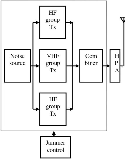
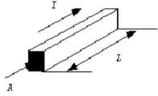
Emitter in Jamming Signal device (also called Radio Jammer) as shown Figure 1, consists of: Frequency monitor, Jammer control, Noise source (Sawtooth generator and or noise generator), Group Tx (HF, VHF, or UHF) consists of exciter a VCO ( Voltage controlled oscillator) or frequency synthesizer and Amplifier, combiner and HPA (high power amplifier).
Exciter is the most important part in jamming signal generation, since the entire signal generation process including sweeper signal, noise signal and the oscillator signal are derived from this part. In this paper, it will be presented an exciter designed using integrated circuit (IC) type MC 1648 a design.
Exciter is the most important part in jamming signal generation, since the entire signal generation process including sweeper signal, noise signal and the oscillator signal are derived from this part. In this paper, it will be presented an
Jammer control
HF group
Tx
VHF group
Tx
HF group
Tx Noise
source
Com biner
H P A
23 exciter designed using integrated circuit (IC) type MC 1648 a
design.
II. EXITERWITHVCO(VOLTAGECONTROLLED OSCILLATOR).
Exciter design is planned to work in the output frequency area of 30 MHz to 80 MHz, which is divided into 20 bands, each band width is 2.5 MHz as shown in figure 2.
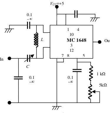
VCO (voltage controlled oscillator) is a form of LC oscillator, as described at figure 3, where the magnitude of output frequency is generated from the control value of capacitance resonant circuit (tank circuit) by an external voltage. Varactor diode, with reverse bias voltage, will result in changes on the capacitance value.
IC MC1648 requires an external parallel tank circuit consisting of inductor (L) and capacitor (C). In addition to inductors and capacitors, MC 1648 requires varaktor diodes. Value of the inductor (L) obtained from the calculation in accordance with the desired frequency. MC1648 IC can be operated at 5.0 Vdc.
The varactor diode receives bias voltage VDC which
causing changes in the capacitance value by CD. When the
resonance is obtained:
0 → 1 1 0
resonance frequency 1 2 . !
Hz
The VCO circuit design was realized using IC type MC1648. As Figure 4.
Output frequency of the VCO (Voltage Controlled
In this paper, exciter design with VCO only for two bands, ie VCO1 with output frequency 30 MHz - 32.5 MHz and VCO2 with output frequency 32.5-35 MHz.
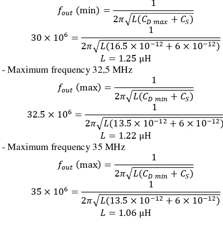
The selection of inductor value is determined based on the magnitude of the following calculation:
CDmaks = 16,5.10-12 F (datasheet varactor diode MV2105)
24 III. FREQUENCYOUTPUTCALCULATION.
Prior to the realization of the circuit, we did the calculation in order to obtain the desired output frequency.
For output Frequency 30 MHz – 32,5 MHz - Minimum frequency 30 MHz
$% &min) 1
2 & *+2 .)
30 4 105 1
2 &16.5 4 108 6 4 108 )
1.25 μH
- Maximum frequency 32,5 MHz
$% &max) 1
2 & *01 .)
32.5 4 105 1
2 &13.5 4 108 6 4 108 )
1.22 μH
- Maximum frequency 35 MHz
$% &max) 1
2 & *01 .)
35 4 105 1
2 &13.5 4 108 6 4 108 )
1.06 μH
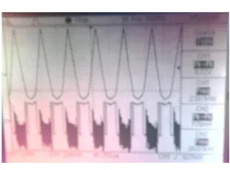
IV. TESTINGANDANALYSIS
Testing was performed aiming to determine the characteristics of the circuit’s output signal. Block diagram of the testing performed is shown in figure 5:
Circuit Testing Result VCO 1 (30 MHz – 32.5 MHz) :
Image signal waveform of a VCO test results (30 MHz - 32.5 MHz) as shown in 6a and 6b.
Figure 6.a. Output Sinyal VCO 1 (min)
Figure 6.b. Output Sinyal VCO 1 (max)
Whereas the graph of the VCO 1 testing results as shown in 7a and b.
Figure 7a. The output frequency characteristics graph vs input voltage VCO 1
0 OUTPUT FREQUENCY GRAPH VS INPUT
VOLTAGE OUTPUT VOLTAGE GRAPH VS OUTPUT
FREQUENCY