1.
Rangkaian Antarmuka Transduser Ultrasonik
3.
Rangkaian Sistem Minimal
Features
• Internally Frequency Compensated for Unity Gain
• Large DC Voltage Gain: 100dB
• Wide Power Supply Range:
LM258/LM258A, LM358/LM358A: 3V~32V (or ±1.5V
~ 16V)
LM2904 : 3V~26V (or ±1.5V ~ 13V)
• Input Common Mode Voltage Range Includes Ground
• Large Output Voltage Swing: 0V DC to Vcc -1.5V DC
• Power Drain Suitable for Battery Operation.
Description
The LM2904,LM358/LM358A, LM258/LM258A consist of
two independent, high gain, internally frequency
compensated operational amplifiers which were designed
specifically to operate from a single power supply over a
wide range of voltage. Operation from split power supplies
is also possible and the low power supply current drain is
independent of the magnitude of the power supply voltage.
Application areas include transducer amplifier, DC gain
blocks and all the conventional OP-AMP circuits which now
can be easily implemented in single power supply systems.
Schematic Diagram
(One section only)
Absolute Maximum Ratings
Parameter
Symbol
LM258/LM258A
LM358/LM358A
LM2904
Unit
Supply Voltage
VCC
±
16 or 32
±
16 or 32
±
13 or 26
V
Differential Input Voltage
VI(DIFF)
32
32
26
V
Input Voltage
VI
-0.3 to +32
-0.3 to +32
-0.3 to +26
V
Output Short Circuit to GND
VCC
≤
15V, TA = 25
°
C(One Amp)
-
Continuous
Continuous
Continuous
Electrical Characteristics
(Vcc = 5.0V, VEE = GND, TA = 25
°
C, unless otherwise specified)
Parameter Symbol
Conditions
LM258
LM358
LM2904
Unit
Min. Typ. Max. Min. Typ. Max. Min. Typ. Max.
Input Offset
(LM2904, VCC=26V)
0
-Vcc
Short Circuit to
Electrical Characteristics
(Continued)(VCC= 5.0V, VEE = GND, unless otherwise specified)
The following specification apply over the range of -25
°
C
≤
TA
≤
+85
°
C for the LM258; and the 0
°
C
≤
TA
≤
+70
°
C
for the LM358; and the -40
°
C
≤
T
A≤
+85
°
C for the LM2904
Parameter
Symbol
Conditions
LM258
LM358
LM2904
Unit
Min. Typ. Max. Min. Typ. Max. Min. Typ. Max.
Electrical Characteristics
(Continued)(VCC = 5.0V, VEE = GND, T
A = 25°
C, unless otherwise specified)
Note:
1. This parameter, although guaranteed, is not 100% tested in production.
Parameter Symbol
Conditions
LM258A
LM358A
Unit
Min. Typ.
Max. Min. Typ.
Max.
Input Offset Voltage
VIO
VCM = 0V to VCC -1.5V
VO(P) = 1.4V, RS = 0
Ω
-
1.0
3.0
-
2.0
3.0
mV
Input Offset Current
IIO
-
-
2
15
-
5
30
nA
Input Bias Current
IBIAS
-
-
40
80
-
45
100
nA
Input Voltage Range
VI(R)
VCC = 30V
0
-
VCC
-1.5
0
-VCC
-1.5
V
Supply Current
ICC
RL =
∞
,VCC = 30V
-
0.8
2.0
-
0.8
2.0
mA
RL =
∞
, VCC = 5V
-
0.5
1.2
-
0.5
1.2
mA
Large Signal Voltage
Gain
GV
VCC = 15V, RL
=
2k
Ω
VO = 1V to 11V
50
100
-
25
100
-
V/mV
Output Voltage Swing
VOH
VCC = 30V
Electrical Characteristics
(Continued)(VCC = 5.0V, VEE = GND, unless otherwise specified)
The following specification apply over the range of -25
°
C
≤
TA
≤
+85
°
C for the LM258A; and the 0
°
C
≤
T
A≤
+70
°
C
for the LM358A
Parameter Symbol
Conditions
LM258A
LM358A
Unit
Min. Typ. Max. Min. Typ. Max.
Input Offset Voltage
VIO
VCM = 0V to VCC -1.5V
VO(P) = 1.4V, RS = 0
Ω
-
-
4.0
-
-
5.0
mV
Input Offset Voltage Drift
∆
VIO/
∆
T
-
-
7.0
15
-
7.0
20
µ
V/
°
C
Input Offset Current
IIO
-
-
-
30
-
-
75
nA
Input Offset Current Drift
∆
IIO/
∆
T
-
-
10
200
-
10
300
pA/
°
C
Input Bias Current
IBIAS
-
-
40
100
-
40
200
nA
Input Common-Mode
Voltage Range
VI(R)
VCC = 30V
0
-Vcc
-2.0
0
-Vcc
-2.0
V
Output Voltage Swing
VO(H)
VCC = 30V
RL = 2k
Ω
26
-
-
26
-
-
V
RL = 10k
Ω
27
28
-
27
28
-
V
VO(L)
VCC = 5V, RL=10k
Ω
-
5
20
-
5
20
mV
Large Signal Voltage Gain
GV
VCC = 15V, RL=2.0k
Ω
VO(P) = 1V to 11V
25
-
-
15
-
-
V/mV
Output Current
ISOURCE
VI(+) = 1V, VI(-) = 0V
VCC = 15V, VO(P) = 2V
10
30
-
10
30
-
mA
ISINK
VI(+) = 1V, VI(-) = 0V
VCC = 15V, VO(P) = 2V
5
9
-
5
9
-
mA
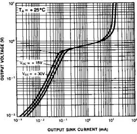
Typical Performance Characteristics
Figure 1. Supply Current vs Supply Voltage Figure 2. Voltage Gain vs Supply Voltage
Figure 3. Open Loop Frequency Response Figure 4. Large Signal Output Swing vs Frequency
Typical Performance Characteristics
(Continued)Figure 7. Input Voltage Range vs Supply Voltage Figure 8. Common-Mode Rejection Ratio
Figure 9. Output Current vs Temperature (Current Limiting) Figure 10. Input Current vs Temperature
Ordering Information
Product Number
Package
Operating Temperature
LM358N
8-DIP
0 ~ +70
°
C
LM358AN
LM358M
8-SOP
LM358AM
LM2904N
8-DIP
-40 ~ +85
°
C
LM2904M
8-SOP
LM258N
8-DIP
-25 ~ +85
°
C
LM258AN
LM258M
LIFE SUPPORT POLICY
FAIRCHILD’S PRODUCTS ARE NOT AUTHORIZED FOR USE AS CRITICAL COMPONENTS IN LIFE SUPPORT DEVICES OR SYSTEMS WITHOUT THE EXPRESS WRITTEN APPROVAL OF THE PRESIDENT OF FAIRCHILD SEMICONDUCTOR CORPORATION. As used herein:
1. Life support devices or systems are devices or systems which, (a) are intended for surgical implant into the body, or (b) support or sustain life, and (c) whose failure to perform when properly used in accordance with
2. A critical component in any component of a life support device or system whose failure to perform can be reasonably expected to cause the failure of the life support device or system, or to affect its safety or effectiveness. DISCLAIMER
www.datasheetcatalog.com
LM193/LM293/LM393/LM2903
Low Power Low Offset Voltage Dual Comparators
General Description
The LM193 series consists of two independent precision voltage comparators with an offset voltage specification as low as 2.0 mV max for two comparators which were de-signed specifically to operate from a single power supply over a wide range of voltages. Operation from split power supplies is also possible and the low power supply current drain is independent of the magnitude of the power supply voltage. These comparators also have a unique characteris-tic in that the input common-mode voltage range includes ground, even though operated from a single power supply voltage.
Application areas include limit comparators, simple analog to digital converters; pulse, squarewave and time delay gen-erators; wide range VCO; MOS clock timers; multivibrators and high voltage digital logic gates. The LM193 series was designed to directly interface with TTL and CMOS. When operated from both plus and minus power supplies, the LM193 series will directly interface with MOS logic where their low power drain is a distinct advantage over standard comparators.
The LM393 and LM2903 parts are available in National’s innovative thin micro SMD package with 8 (12 mil) large bumps.
Advantages
n High precision comparators
n Reduced VOSdrift over temperature
n Eliminates need for dual supplies
n Allows sensing near ground
n Compatible with all forms of logic
n Power drain suitable for battery operation
Features
n Wide supply— Voltage range: 2.0V to 36V — Single or dual supplies: ±1.0V to±18V
n Very low supply current drain (0.4 mA) — independent
of supply voltage
n Low input biasing current: 25 nA
n Low input offset current: ±5 nA
n Maximum offset voltage: ±3 mV
n Input common-mode voltage range includes ground
n Differential input voltage range equal to the power supply voltage
n Low output saturation voltage,: 250 mV at 4 mA
n Output voltage compatible with TTL, DTL, ECL, MOS and CMOS logic systems
n Available in the 8-Bump (12 mil) micro SMD package
n See AN-1112 for micro SMD considerations
Squarewave Oscillator Non-Inverting Comparator with Hysteresis
00570902
Metal Can Package Dual-In-Line/SOIC Package
00570903
00570901
micro SMD micro SMD Marking
00570945
Top View 00570946
Top View
Absolute Maximum Ratings
(Note 10)If Military/Aerospace specified devices are required, please contact the National Semiconductor Sales Office/ Distributors for availability and specifications.
Supply Voltage, V+ 36V
Differential Input Voltage (Note 8) 36V Input Voltage −0.3V to +36V Input Current (VIN
<
−0.3V) (Note 3) 50 mAPower Dissipation (Note 1)
Molded DIP 780 mW Metal Can 660 mW Small Outline Package 510 mW micro SMD Pacakge 568mW Output Short-Circuit to Ground
(Note 2) Continuous Operating Temperature Range
LM393 0˚C to +70˚C LM293 −25˚C to +85˚C
LM193/LM193A −55˚C to +125˚C LM2903 −40˚C to +85˚C Storage Temperature Range −65˚C to +150˚C Lead Temperature
(Soldering, 10 seconds) +260˚C Soldering Information
Dual-In-Line Package
Soldering (10 seconds) 260˚C Small Outline Package 215˚C
Vapor Phase (60 seconds)
Infrared (15 seconds) 220˚C See AN-450 “Surface Mounting Methods and Their Effect on Product Reliability” for other methods of soldering surface mount devices.
ESD rating
(1.5 kΩin series with 100 pF) 1300V
Electrical Characteristics
(V+=5V, T
A= 25˚C, unless otherwise stated)
Parameter Conditions LM193A Units
Min Typ Max
Input Offset Voltage (Note 9) 1.0 2.0 mV Input Bias Current IIN(+) or IIN(−) with Output In Linear 25 100 nA
Large Signal Response VIN=TTL Logic Swing, VREF=1.4V 300 ns Time VRL=5V, RL=5.1 kΩ
A= 25˚C, unless otherwise stated)
Parameter Conditions LM193 LM293, LM393 LM2903 Units
Min Typ Max Min Typ Max Min Typ Max
Input Offset Voltage (Note 9) 1.0 5.0 1.0 5.0 2.0 7.0 mV Input Bias Current IIN(+) or IIN(−) with Output In 25 100 25 250 25 250 nA
Linear Range, VCM= 0V (Note 5)
Input Offset Current IIN(+)−IIN(−) VCM= 0V 3.0 25 5.0 50 5.0 50 nA
(V+=5V, T
A= 25˚C, unless otherwise stated)
Parameter Conditions LM193 LM293, LM393 LM2903 Units
Min Typ Max Min Typ Max Min Typ Max
Supply Current RL=∞ V+=5V 0.4 1 0.4 1 0.4 1.0 mA
V+=36V 1 2.5 1 2.5 1 2.5 mA
Voltage Gain RL≥15 kΩ, V+=15V 50 200 50 200 25 100 V/mV
VO= 1V to 11V
Large Signal Response VIN=TTL Logic Swing, VREF=1.4V 300 300 300 ns
Time VRL=5V, RL=5.1 kΩ
Parameter Conditions LM193A Units
Min Typ Max
Input Offset Voltage (Note 9) 4.0 mV Input Offset Current IIN(+)−IIN(−), VCM=0V 100 nA
Input Bias Current IIN(+) or IIN(−) with Output in Linear Range, 300 nA
VCM=0V (Note 5)
Differential Input Voltage Keep All VIN’s≥0V (or V−, if Used), (Note 8) 36 V
Electrical Characteristics
(V+ = 5V) (Note 4)
Parameter Conditions LM193 LM293, LM393 LM2903 Units
Min Typ Max Min Typ Max Min Typ Max
Input Offset Voltage (Note 9) 9 9 9 15 mV Input Offset Current IIN(+)−IIN(−), VCM=0V 100 150 50 200 nA
Input Bias Current IIN(+) or IIN(−) with Output in
Linear Range, VCM=0V
(Note 5)
300 400 200 500 nA
Input Common Mode Voltage Range
V+=30V (Note 6) 0 V+−2.0 0 V+−2.0 0 V+−2.0 V
Saturation Voltage VIN(−)=1V, VIN(+)=0,
ISINK≤4 mA
700 700 400 700 mV
Output Leakage Current VIN(−)=0, VIN(+)=1V, VO=30V 1.0 1.0 1.0 µA
Differential Input Voltage Keep All VIN’s≥0V (or V−, if
Used), (Note 8)
36 36 36 V
Note 1: For operating at high temperatures, the LM393 and LM2903 must be derated based on a 125˚C maximum junction temperature and a thermal resistance of 170˚C/W which applies for the device soldered in a printed circuit board, operating in a still air ambient. The LM193/LM193A/LM293 must be derated based on
Electrical Characteristics
(Continued)on the IC chip. This transistor action can cause the output voltages of the comparators to go to the V+voltage level (or to ground for a large overdrive) for the time
duration that an input is driven negative. This is not destructive and normal output states will re-establish when the input voltage, which was negative, again returns to a value greater than −0.3V.
Note 4: These specifications are limited to −55˚C≤TA≤+125˚C, for the LM193/LM193A. With the LM293 all temperature specifications are limited to
−25˚C≤TA≤+85˚C and the LM393 temperature specifications are limited to 0˚C≤TA≤+70˚C. The LM2903 is limited to −40˚C≤TA≤+85˚C.
Note 5: The direction of the input current is out of the IC due to the PNP input stage. This current is essentially constant, independent of the state of the output so no loading change exists on the reference or input lines.
Note 6: The input common-mode voltage or either input signal voltage should not be allowed to go negative by more than 0.3V. The upper end of the common-mode
voltage range is V+−1.5V at 25˚C, but either or both inputs can go to 36V without damage, independent of the magnitude of V+.
Note 7: The response time specified is for a 100 mV input step with 5 mV overdrive. For larger overdrive signals 300 ns can be obtained, see typical performance characteristics section.
Note 8: Positive excursions of input voltage may exceed the power supply level. As long as the other voltage remains within the common-mode range, the comparator will provide a proper output state. The low input voltage state must not be less than −0.3V (or 0.3V below the magnitude of the negative power supply, if used).
Note 9: At output switch point, VO.1.4V, RS=0Ωwith V+from 5V to 30V; and over the full input common-mode range (0V to V+−1.5V), at 25˚C.
Note 10:Refer to RETS193AX for LM193AH military specifications and to RETS193X for LM193H military specifications.
Ordering Information
Package Temperature Range Part Number NSC Drawing
8-Pin Metal Can −25˚C to 85˚C LM293H
0˚C to 70˚C LM393H
8-Pin Ceramic DIP −55˚C to 125˚C
LM193J/883*
J08A LM193AJ/883
LM193AJ-QMLV**
LM193AJ-MLS
8-Pin Molded DIP 0˚C to 70˚C LM393N N08E −40˚C to 85˚C LM2903N
8-Pin SOIC
0˚C to 70˚C LM393M
M08A LM393MX
−40˚C to 85˚C LM2903M LM2903MX
8-Bump (12 mils) micro SMD
0˚C to 70˚C LM393TL
TLA08AAA LM393TLX
−40˚C to 85˚C LM2903ITL LM2903ITLX
Note:*Also available per LM38510/11202
Supply Current Input Current
00570925 00570926
Output Saturation Voltage
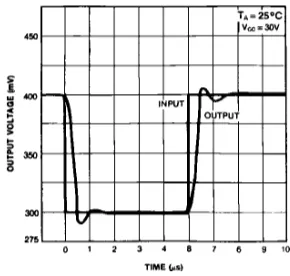
Response Time for Various Input Overdrives — Negative Transition
00570927 00570928
Response Time for Various Input Overdrives — Positive Transition
00570929
Typical Performance Characteristics
LM2903Supply Current Input Current
00570930 00570931
Output Saturation Voltage
Response Time for Various Input Overdrives — Negative Transition
00570932
00570933
Response Time for Various Input Overdrives — Positive Transition
The LM193 series are high gain, wide bandwidth devices which, like most comparators, can easily oscillate if the output lead is inadvertently allowed to capacitively couple to the inputs via stray capacitance. This shows up only during the output voltage transition intervals as the comparator change states. Power supply bypassing is not required to solve this problem. Standard PC board layout is helpful as it reduces stray input-output coupling. Reducing the input re-sistors to
<
10 kΩreduces the feedback signal levels and finally, adding even a small amount (1.0 to 10 mV) of positive feedback (hysteresis) causes such a rapid transition that oscillations due to stray feedback are not possible. Simply socketing the IC and attaching resistors to the pins will cause input-output oscillations during the small transition intervals unless hysteresis is used. If the input signal is a pulse waveform, with relatively fast rise and fall times, hysteresis is not required.All input pins of any unused comparators should be tied to the negative supply.
The bias network of the LM193 series establishes a drain current which is independent of the magnitude of the power supply voltage over the range of from 2.0 VDCto 30 VDC. It is usually unnecessary to use a bypass capacitor across the power supply line.
The differential input voltage may be larger than V+without
damaging the device (Note 8). Protection should be provided to prevent the input voltages from going negative more than −0.3 VDC(at 25˚C). An input clamp diode can be used as shown in the applications section.
The output of the LM193 series is the uncommitted collector of a grounded-emitter NPN output transistor. Many collectors can be tied together to provide an output OR’ing function. An output pull-up resistor can be connected to any available power supply voltage within the permitted supply voltage range and there is no restriction on this voltage due to the magnitude of the voltage which is applied to the V+terminal
of the LM193 package. The output can also be used as a simple SPST switch to ground (when a pull-up resistor is not used). The amount of current which the output device can sink is limited by the drive available (which is independent of V+) and theβof this device. When the maximum current limit
is reached (approximately 16mA), the output transistor will come out of saturation and the output voltage will rise very rapidly. The output saturation voltage is limited by the ap-proximately 60ΩrSATof the output transistor. The low offset
voltage of the output transistor (1.0mV) allows the output to clamp essentially to ground level for small load currents.
Typical Applications
(V+=5.0 V DC)Basic Comparator Driving CMOS Driving TTL
00570935
00570936 00570937
Squarewave Oscillator Pulse Generator Crystal Controlled Oscillator
00570938
00570939 * For large ratios of R1/R2,
D1 can be omitted.
00570940
Typical Applications
(V+=5.0 VDC) (Continued)
Two-Decade High Frequency VCO
00570941 V*= +30 VDC
+250 mVDC≤VC≤+50 VDC 700Hz≤fo≤100kHz
Basic Comparator Non-Inverting Comparator with Hysteresis
00570906
00570909
Inverting Comparator with Hysteresis Output Strobing
00570910
AND Gate OR Gate
00570912
00570913
Large Fan-in AND Gate Limit Comparator
00570914
00570915
Comparing Input Voltages of Opposite Polarity ORing the Outputs
00570916
00570917
Typical Applications
(V+=5.0 VDC) (Continued)
Zero Crossing Detector (Single Power Supply) One-Shot Multivibrator
00570921 00570922
Bi-Stable Multivibrator One-Shot Multivibrator with Input Lock Out
00570924
00570923
Zero Crossing Detector Comparator With a Negative Reference
Time Delay Generator
00570907
Split-Supply Applications
(V+=+15 VDCand V−=−15 VDC)
MOS Clock Driver
00570942
Physical Dimensions
inches (millimeters) unless otherwise notedMetal Can Package (H) NS Package Number H08C
SOIC Package NS Package Number M08A
Molded Dual-In-Line Package (N) NS Package N08E
Physical Dimensions
inches (millimeters) unless otherwise noted (Continued)NOTE: UNLESS OTHERWISE SPECIFIED
1. EPOXY COATING
2. 63Sn/37Pb EUTECTIC BUMP
3. RECOMMEND NON-SOLDER MASK DEFINED LANDING PAD.
4. PIN A1 IS ESTABLISHED BY LOWER LEFT CORNER WITH RESPECT TO TEXT ORIENTATION REMAINING PINS ARE NUMBERED COUNTERCLOCKWISE.
5. XXX IN DRAWING NUMBER REPRESENTS PACKAGE SIZE VARIATION WHERE X1IS PACKAGE WIDTH, X2IS PACKAGE LENGTH AND X3IS PACKAGE HEIGHT.
6. REFERENCE JEDEC REGISTRATION MO-211, VARIATION BC.
8-Bump (12 mil) micro SMD Package NS Package TLA08AAA
X1 = 1.514mm X2 = 1.514mm X3= 0.600mm
LIFE SUPPORT POLICY
NATIONAL’S PRODUCTS ARE NOT AUTHORIZED FOR USE AS CRITICAL COMPONENTS IN LIFE SUPPORT DEVICES OR SYSTEMS WITHOUT THE EXPRESS WRITTEN APPROVAL OF THE PRESIDENT AND GENERAL COUNSEL OF NATIONAL SEMICONDUCTOR CORPORATION. As used herein:
1. Life support devices or systems are devices or systems which, (a) are intended for surgical implant into the body, or (b) support or sustain life, and whose failure to perform when properly used in accordance with instructions for use provided in the labeling, can be reasonably expected to result in a significant injury to the user.
Open, Enclosed, Pulse Transit, Wide Bandwith and Built-in Crystal Oscillator Types
Ultrasonic Ceramic Transducers transfer
acoustical energy to mechanical energy or vice
versa
The
Standard Open Type
Transducer is
con-structed in a manner which incorporates the
fundamental structure of a piezoelectric
ceramic element of the monomorph type with a
conical metal resonator. This special
combination provides high sensitivity (over
-65dB/V/µ Bar), wider bandwidth, excellent
temperature and humidity durability, stable
electrical and mechanical characteristics, and
small size.
The
Standard Enciosed Type Transducer
can
be used for outdoor installation, or, because of
its special dust-proof construction, can be used
in a dusty atmosphere. The unit has a vibrating
diaphragm, consisting of one piezoelectric
ceramic element inside an metal case. The back
of the transducer is completely sealed with
resin. It can not be used under water, although
it is
complete enclosed.
The
Pulse Transit Type Transducer
has been
The
Wide Bandwidth Type Transducer
utilizes
the resonance of a piezoelectric bender and the
resonant effect of a speciai design c o n e . This
provides
a
wide zone of operation and is .
suitable not only as a multi-function remote
:;on-trol device, but also as an intrusion alarm
sys-tem or for any other application which
a wide
Ope ra t ingfrequency
of
transmitting and receiving man y signal
trequen-cies.
The
Built-in Oscillator
Type Transmitter
be directly drived by the DC voltage starting
from DC 2 Volts to DC 7 Volts
A
driving
chip and a 30ppm tuning fork type
crys-tal are built-in with open and enclosed type
to ensure a precise
and
uniform Sound pressure output. Continual
Sound output or pulsing sound Output is
avail-able upon request.
Electrical & Mechanical
Specifica-tions and Model Numbers:
2 3 4 5
Dimensions - Open Typ
Remarks:
1. Center Frequency in 10 2 Hz
2.
Types:S:
Open Type;E:
Enclosed TypeC:
Oscillator Built-in (DC) Type3. Applications: Transmitter, R:
P:
Pulse Transit,W:
Wide Bandwidth 4. Gase Dimensions: in mm.5; Remarks:
P:
Piastic Housing,B:
Black Hous-ingDimensions are in mm, ( ) are in inch
e
Tolerance : 0.5
Electrical Specifications - Open Type
-67dB
117dB
20
10
-70dB 112dB
Performance Characteristics
Frequency Characteristics
Sensitvity
Transmitter: Sound Pressure Level
Impedance and Phase Angle
t
i i i
i
Characteristics Change Due to Load Resistance
Characteristic Change Due to Input Voltage
.
. . . .
- 9 0
35 40 45
F R E Q U E N C Y
0.1 1
INPUT VOLTAGE
Frequency Shift Due to Input Voltage
AF
RATION: Fn: F2 AF
F n : P E A K F R E Q U E N C Y O N N V I N P U T F R E Q U E N C Y O N 2 V I N P U T
0.1
10 50I N P U T V O L T A G E
Humidity Characteristics And Shock Test
Temperature Characteristics
BEFORE TEST
-A F T E R TEST
F R E Q U E N C Y
Durability
Temperature Cycle and Vibration Test
FOR CENTER FREQUENCY A X 100
BEFORE TEST w w
-A F T E R C YC L E T EST
t
A : DIFFERENT VALUE 0 : ORINAL VALUE
37 43
Diescr mit dem eine viclscitig vcrwcndbare drahtlose Fcrnbcdicnung.
langsam so lange verstellt, bis das
eingenommenen
ZustandD a m i t
ist
h ö c h s t ekcit des Nach Einschal-ten d c s Senders muß sich das Relais vom
destens IO cm Nach richtiger
von P l s i c h d e r A b s t a n d Typ, jedoch sollte für Sender und
die Ausführung verwendet wcrdcn.
x U S - M i k r o f o n
M A 4 0H A 4 0