EFFECT OF DEPOSITION TIME ON THE STRUCTURAL AND
OPTICAL PROPERTIES OF MOLYBDENUM CHALCOGENIDES
THIN FILMS
S. SHARIZA AND T. JOSEPH SAHAYA ANAND*
*Corresponding author: [email protected]
Department of Engineering Materials, Faculty of Manufacturing Engineering, Universiti Teknikal Malaysia Melaka, Durian Tunggal, 76100 Melaka, Malaysia
Molybdenum chalcogenides, specifically molybdenum selenide, MoSe2 and molybdenum sulphide, MoS2 thin films have been successfully deposited onto indium-tin-oxide (ITO) coated glass substrates and stainless steel substrates by electrodeposition technique. The effects of the deposition time on the growth, structural and optical properties of the films were then studied. X-ray diffraction (XRD) patterns have confirmed the polycrystalline rhombohedral MoSe2 and hexagonal MoS2 phase formation. The results show that the intensity of XRD peaks for these materials increases with the increase of deposition time. UV -VIS spectrophotometric measurement revealed that the optical band gap values of the thin films decreased with the increase of deposition time and lie in the range from 1.12 – 1.22 eV for MoSe2 and 1.65 – 1.74 eV for MoS2 thin films. Surface morphology studies by scanning electron microscopy showed uniform and continuous thin film with layered structure surface.
(Received July 25; 2011; accepted August 29, 2011)
Keywords: Molybdenum chalcogenides, Electrodeposition, X-ray diffraction, UV-VIS spectrophotometer, Scanning electron microscope
1. Introduction
The preparation of thin film materials opens the opportunity of observing the evolution of physical properties of the materials with sizes [1]. The reduction of sizes, in terms of thickness of the thin film provide the possibility of observing novel behaviours such as size dependent structural, electrical and optical properties [2]. Concurrently, the preparation of transition metal chalcogenides (TMC) has been done extensively for its high potential use in the non-conventional energy resources industries [3-4]. In recent years, TMC compounds such as CdHgSe, ZrSe2, CdSeTe, WSSe, and CdS have been actively investigated for photoelectrochemical (PEC) and solar cell applications [5-9].
Generally, TMC compounds can be obtained in thin film form by various methods, including sputtering [2], chemical bath deposition [10], selenization [13], solid state reaction [14], sulphurization [15] and electrolytic reduction [16]. However, they are cost intensive and sometimes present special problems for the preparation of transition metal chalcogenide films [17]. Aside from this, the electrodeposition method offers simplicity and economy, control of film thickness, uniformity and possibility of deposition of thin films onto substrates of large and complex shape [18].
2. Experimental details
2.1 Electrodeposition of molybdenum chalcogenide thin films
The electrodeposition of the molybdenum chalcogenide (both MoSe2 and MoS2) thin films was carried out using a Princeton Applied Research Model VersaSTAT 3 Potentiostat. The deposition potential of the molybdenum chalcogenide thin film was first derived from cyclic voltammetry (CV) technique followed by synthesis of the chalcogenides by electrodeposition technique.
A three – electrode cell system was adopted for the cyclic voltammetry analysis and deposition of the film as shown in Fig. 1. The electrolysis cell consisted of (i) an ITO-coated glass substrate or stainless steel substrate as the working electrode (WE) on which the molybdenum chalcogenide thin film is to be deposited; (ii) graphite as the counter electrode (CE); and (iii) a saturated calomel electrode (SCE) with Ag/AgCl reference system as the reference electrode [19]. The SCE measures the potential of the working electrode. The electrode spacing should be carefully adjusted to obtain good results. Both working and counter electrodes are kept as close as 1 cm to each other and the two surfaces facing each other were kept parallel, so that released ions will be attracted and deposited exactly perpendicular to the cathode surface. The reference electrode tip is placed very close to the cathode surface so that the exact potential at the surface will be monitored unaffected by the solution resistance (internal resistance of the cell).
Fig. 1. Electrolysis cell setup for molybdenum chalcogenide thin film deposition.
For the deposition of molybdenum selenide, MoSe2 and molybdenum sulphide, MoS2 thin films, an ammoniacal solution consisting of a mixture of molybdic acid and selenium dioxide (H2MoO4 + SeO2) and molybdic acid and sodium thiosulphate pentahydrate (H2MoO4 + Na2S2O3.5H2O) was used as electrolyte, respectively. The deposition of films was carried out at a temperature of 40 ± 1 °C for 30 minutes. To prepare electrolyte solutions having relative concentrations of H2MoO4 and SeO2, the following two basic solutions were first prepared: solution A containing H2MoO4 in ammonia and solution B containing SeO2 in water. Equal volumes of these two basic solutions were mixed to obtain the electrolysis solutions. The similar procedure was followed for the electrolyte solutions of H2MoO4 and Na2S2O3.5H2O.
2.2 Characterization of thin films
The X-ray diffractograms of the thin film was obtained on a PANalytical XPERT PROMPD PW 3040/60 diffractometer using monochromatic CuKαradiation (λ = 1.5405 Å) in the
range of 2θ angles from 10º – 90º. The metal chalcogenide’s crystallographic properties such as
3. Results and discussion
3.1 Electrodeposition and physical properties of films
Cyclic voltammetry (CV) test was carried out before the deposition process. It was done between two potential limits (-1.00 V to 1.00 V) for the solutions prepared to probe the prospective potentials for deposition of the thin films. The solutions are those of the mixture of ammoniacal H2MoO4 + SeO2 (solution A) and the mixture of ammoniacal H2MoO4 + Na2S2O3.5H2O (solution B) for the deposition of MoSe2 and MoS2, respectively. The Electrochemical Analysis System Software (PAR Versa Studio 2.0) was used to control the deposition process and to monitor the current and voltage profiles.
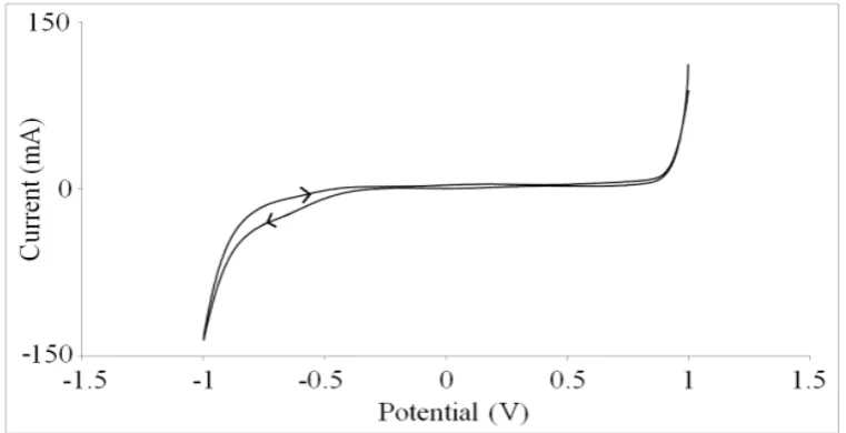
Fig. 2 and 3 shows the cyclic voltammogram of the electrodes in solutions A and B for MoSe2 and MoS2, respectively. As shown in Fig. 2, the forward scan almost immediately dropped and remained constant until a current drop at -0.5 V suggesting a reduction process. The current change is associated with the reduction of molybdenum and selenide ions to form solid molybdenum selenide, MoSe2 compound on the substrate. The deposition of molybdenum selenide on the substrate continued until the equilibrium potential is achieved at an interception between the forward and reverse scan at approximately -0.1 V versus Ag/AgCl.
Fig. 2. Cyclic voltammogram of the electrodes in ammoniacal H2MoO4 + SeO2 solution
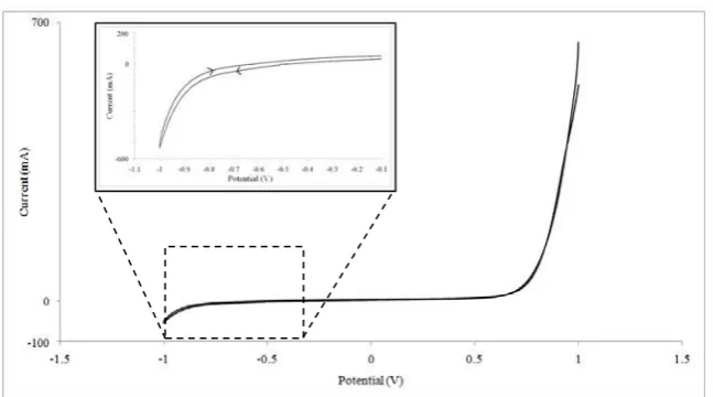
Fig. 3. Cyclic voltammogram of the electrodes in ammoniacal H2MoO4 + Na2S2O3.5H2O solution.
From the results obtained through CV measurements of the system, the deposition of MoSe2 and MoS2 thin films on ITO-coated glass substrates and stainless steel substrates were carried out at the selected potential -1.0 V versus Ag/AgCl. The deposition temperature of the thin films were set and controlled at 40 °C ± 1 °C while the deposition time of the thin films was set at 10, 15, 20, 25 and 30 minutes for both compounds.
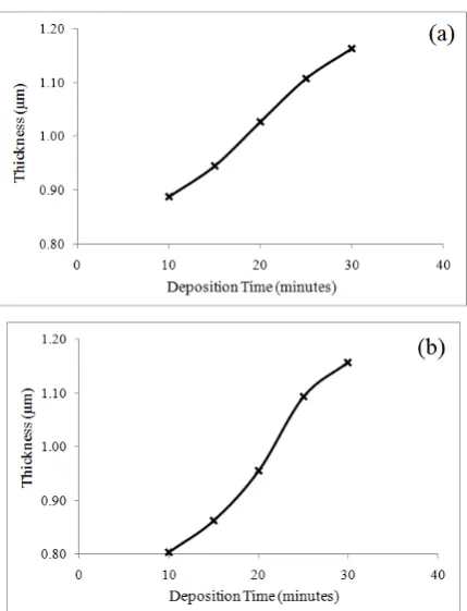
From the above reactions, it appears that an increase in the film thickness is expected as the deposition times are increased. A plot of thickness versus deposition times for both types of films is displayed in Fig. 4. The thickness of the thin films were calculated by using the relation between mass and volume in the density calculation, where density is equal to the value of mass over the volume as in equation below.
Fig. 4. Variation of thickness with deposition time for (a) MoSe2, (b) MoS2 films
3.2 Structural Characterization
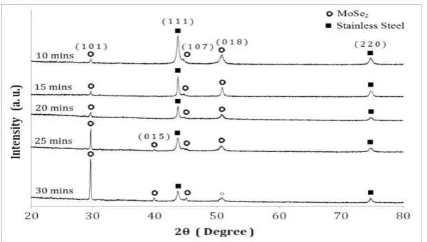
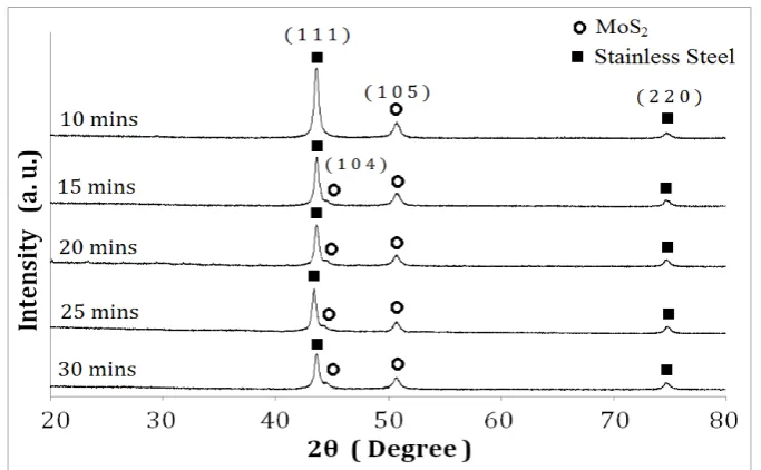
X-ray diffraction (XRD) patterns of the electrodeposited molybdenum selenide, MoSe2 and molybdenum sulphide, MoS2 thin film on stainless steel substrate is shown in Fig. 5 and 6. Films on stainless steel substrates were characterized for XRD due to the amorphous feature that was obtained when characterizing the films on ITO-coated glass substrates. XRD peaks, identified in the figure, have been indexed with the help of the Joint Committee of Powder Diffraction Standards (JCPDS) file and the corresponding XRD data values are summarized in Table 1 and 2 for MoSe2 and MoS2 thin films, respectively.
Fig. 5. X-ray diffraction pattern for MoSe2 thin films deposited at different deposition times.
Peaks belonging to MoSe2 are detected for the films prepared at all the deposition times investigated. However, it can be seen in the figure that at 10 minutes deposition time of MoSe2, the peak for the stainless steel substrate are more prominent in intensity comparing to MoSe2 peaks. As deposition time increase, the peaks of MoSe2 especially at 2θ = 29.5° and 45.1° become more prominent indicating that the (101) and (107) plane films grow with time. Also, at deposition time 25 minutes and 30 minutes, a MoSe2 film having (015) plane structure emerges at 2θ = 39.8°. The stainless steel peak at 2θ = 43.6° which is the most intense peak at 10 minutes have shrunk at deposition time 30 minutes due to the growth of (107) plane films which has surmount over the stainless steel peaks. As for the (018) plane structure of MoSe2 at 2θ = 50.8° and (220) plane
structure of stainless steel at 2θ = 74.7°, the deposition time does not have any influence on them,
as they appear as constant peaks for the thin films deposited at time 10 minutes up to 30 minutes. The interplanar distances‘d’ corresponding to different h k l planes were calculated from the X-ray diffractograms and are recorded in Table 1. The crystallite size was calculated from the measurement of full-width at half-maximum (FWHM) in different X-ray peaks and values are in the range of 45 – 65 nm.
Table 1: Comparison of experimental’d ' values with JCPDS data for MoSe2 thin film on stainless steel
substrate with different deposition time
Fig. 6. X-ray diffraction pattern for MoS2 thin films deposited at different deposition times
For MoSe2 thin films deposited at deposition time of 10 – 30 minutes, peaks belonging to MoS2 are detected. However, it can be seen in the figure that at 10 minutes deposition time, only one peak identified as MoS2 peak is present at 2θ = 50.1° while the peaks for the stainless steel are more visible. However, at 15 minutes deposition time, a MoS2 peak at 2θ = 44.4° start to emerge and become more distinct from the neighbouring peak indicating that the (104) plane films grow
with time. The stainless steel peak at 2θ = 43.6° which is most intense at 10 minutes have shrunk
at deposition time 30 minutes due to the growth of (104) plane films which has surmount over the stainless steel peaks. As for the (105) plane structure of MoS2 at 2θ = 50.1° and (220) plane
structure of stainless steel at 2θ = 74.7°, the deposition time does not have any influence on the
thin films, as they appear as constant peaks throughout.
Table 2: Comparison of experimental‘d’ values with JCPDS data for MoS2 thin film on stainless steel
substrate with different deposition time
3.3 Optical Characterization
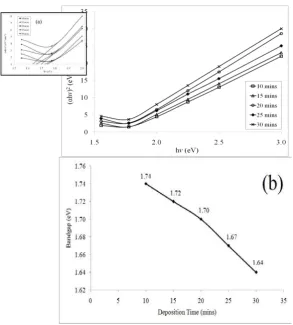
The transition metal chalcogenides are usually indirect band gap semiconductors [23]. The optical absorption spectrum was taken for both MoSe2 and MoS2 thin film using an identical ITO-coated glass plate as reference. A graph of (αhv) 2 vs. hv is drawn and the linear portion of the graph is extrapolated to the energy axis. The intercepts on the energy axis at α=0 gives the band gaps of these compounds.
For the MoS2 thin films, the (αhv) 2 versus hv plots of the deposited films at different deposition times is shown in Fig. 8(a) (see inset graph). Fig. 8(b) presents the non-linear decrease for the variation of band gap energy (Eg) with different deposition time. The figure shows that the Eg decreased from 1.74 eV to 1.64 eV with increase of deposition time for the MoS2 thin films, in good range with the reported value [25].
Fig. 7. Variation of MoSe2 thin films deposited at different deposition times. (a) (αhv) 2
vs. hv and (b) bandgap vs.deposition time
Fig. 8. Variation of MoS2thin films deposited at different deposition times. (a) (αhv)2 vs. hv and
3.4 Morphological Characterization
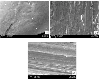
The surface morphology of the MoSe2 and MoS2 thin films were determined by scanning electron microscope (SEM). The SEM micrograph of the MoSe2 and MoS2 thin film deposited on indium-tin-oxide (ITO) glass substrates at different deposition time is shown in Figure 9(a) - 9(c) and Figure 10(a) - 10(c).
Fig. 10. Surface morphology of MoS2 thin film deposited at (a) 10 (b) 20 and (c) 30 minutes
From SEM analysis, as deposition time increases, the surface of the MoSe2 and MoS2 thin films are clearly seen to be in layered structure. At deposition time 30 minutes, the surface of the thin film is found to be the best with a uniform and continuous morphology.
4. Conclusion
Using electrodeposition technique, molybdenum chalcogenide, MoSe2 and MoS2 thin films were successfully deposited on indium-tin-oxide; ITO-coated glass substrates and stainless steel substrates in which the deposition time for the thin films were optimized from 10 minutes to 30 minutes. The best stoichiometric film were deposited at an optimized deposition potential of -1.0 VSCE with deposition time 30 minutes, keeping the bath at temperature 40 ± 1 °C. The XRD pattern shows that the thin films are polycrystalline in nature. The optical band energy values for the thin films were extrapolated and found to decrease with increasing deposition time. SEM photograph shows that the thin films are uniform and continuous with a layered structure for the thin films deposited at 30 minutes.
Acknowledgement
References
[1] R. S. Mane, Sankapal, B. R., Lokhande, C. D., Mater. Chem. Phys. 64, 215 (2000).
[2] Ghosh, P. K., Ahmed, Sk. F, Saha, B., Chattopadhyay, K. K., presented at the International Workshop on Physics of Semiconductor Devices, December 16 – 20, 2007, Mumbai, India. [11] Ghosh, P. K., Mitra, M. K., Chattopadhyay, K. K., Nanotech. 16, 107 (2005).
[12] Huang, N. M., Radiman, S., Lim, H. N., Yeong, S. K., Khiew, P. S., Chiu, W. S., Mohamed Saeed, G. H., Nadarajah, K., Chem. Eng. J. 147, 399 (2009).
[13] Joseph Sahaya Anand, T., Senthil, K
[14] Pouzet, J., Hadouda, H., Bernede, J. C., Leny, R., J. Phys. Chem. Solids 57, 1363 (1996). [15] Jäger-Waldau, A., Lux-Steiner, M. Ch., Bucher, E., Scandell, L., Schumacher, A., Prins, R., App. Surf. Sc. 65-66, 465 (1993).
[16] Ponomarev, E. A., Neumann-Spallart, M., Hodes, G., Lévy-Clément, C., Thin Sol. Films 280, 86 (1996).
[17] Srivastava, S. K., Palit, D., Sol. St. Ionics 176, 513 (2005).
[18] Habib M. Pathan, Sun-Ki Min, Kwang-Deog Jung, Oh-Shim Joo, Electrochem. Comm. 8, 273 (2006).
[19] Zainal, Z., Saravanan, N., Mien, H. L., J. Mater. Sc.: Mater. in Electronics 16, 111 (2005). [20] JCPDS, ICDD, Card No. 33-397.
[21] JCPDS, ICDD, Card No. 1-72-1420. [22] JCPDS, ICDD, Card No. 2-1133.
[23] Roy, P., Srivastava, S. K., Thin Sol. Films 496, 293 (2006). [24] Vora, M. M., Vora, A. M., Chalc. Lett 4, 97 (2007).