Broadband Microwave
Amplifiers
Bal S. Virdee
Avtar S. Virdee
Ben Y. Banyamin
A catalog record of this book is available from the Library of Congress.
British Library Cataloguing in Publication Data
A catalog of this book is available from the British Library.
Cover design by Gary Ragaglia
© 2004 ARTECH HOUSE, INC. 685 Canton Street
Norwood, MA 02062
All rights reserved. Printed and bound in the United States of America. No part of this book may be reproduced or utilized in any form or by any means, electronic or mechanical, includ-ing photocopyinclud-ing, recordinclud-ing, or by any information storage and retrieval system, without permission in writing from the publisher.
All terms mentioned in this book that are known to be trademarks or service marks have been appropriately capitalized. Artech House cannot attest to the accuracy of this informa-tion. Use of a term in this book should not be regarded as affecting the validity of any trade-mark or service trade-mark.
International Standard Book Number: 1-58053-892-4
Contents
Foreword ix
Preface xi
Organization of This Book xii
Acknowledgments xv
CHAPTER 1
Overview of Broadband Amplifiers 1
1.1 Historical Perspective on Microwave Amplifiers 1
1.2 Broadband Amplifiers 3
1.3 Review of Various Broadband Amplifiers 3
1.3.1 Reactively Matched Amplifiers 4
1.3.2 TWDAs 5
1.3.3 Broadband Feedback and Lossy Matched Amplifiers 8
1.3.4 CSSDAs 10
References 14
CHAPTER 2
Principles and Applications of Distributed Amplifiers 17
2.1 Introduction 17
2.2 Heterojunction Field Effect Transistor 17
2.3 Conventional TWDA 20
2.3.1 Available Gain of a TWDA 21
2.3.2 Advantages of TWDA 26
2.3.3 Disadvantages of TWDA 27
2.4 CSSDA 27
2.4.1 Lossless CSSDA 28
2.4.2 Available Power Gain of the Lossless CSSDA 29
2.4.3 Analysis of Interstage Characteristic Impedance on the
Lossless CSSDA 32
2.4.4 Output Current of the CSSDA 33
2.4.5 Output Voltage of the CSSDA 35
2.4.6 Lossy CSSDAs 36
2.4.7 Characteristic Features of CSSDA 38
2.5 Other Applications of Distributed Amplifiers 41
2.5.1 Applications of TWDA 41
2.6 Potential Applications of CSSDA 48
2.6.1 Oscillator 48
2.6.2 Optical Driver 48
2.6.3 Optical Receiver 48
References 50
CHAPTER 3
Device Structure and Mode of Operation 51
3.1 Introduction 51
3.2 The GaAs MESFET—Structure and Operation 51
3.3 HEMT-based Devices—Structure and Operation 54
3.3.1 HEMT 54
3.3.2 SPHEMT 56
3.3.3 DPHEMT 58
3.4 Summary 61
References 61
CHAPTER 4
Device Characterization and Modeling 63
4.1 Introduction 63
4.2 Device Characterization 63
4.2.1 Basis of Calibration 64
4.2.2 Microstrip Test Fixture and Calibration Standards 65
4.2.3 Small-Signal Measurements 68
4.2.4 Pulsed dc I–V Measurements 74
4.3 Small-Signal Device Modeling 81
4.3.1 Principle of Model Extraction Procedure 82
4.3.2 Extraction of Cold Component Values 83
4.3.3 Extraction of Hot Components Values 85
4.3.4 Small-Signal Modeling 86
4.4 Large-Signal Device Modeling 90
4.4.1 Large-Signal Device Model 91
4.4.2 Nonlinear Analysis Techniques 91
4.4.3 Large-Signal Modeling Techniques 93
4.4.4 Modeled and Measured Results 98
References 100
CHAPTER 5
Amplifier Class of Operation 103
5.1 Introduction 103
5.3 Class B Amplifiers 109
5.4 Class AB Amplifiers 113
References 117
CHAPTER 6
Design of Broadband Microwave Amplifiers 119
6.1 Introduction 119
6.2 Multistage Broadband Amplifier Design 120
6.3 Output Power and Power-Added Efficiency 121
6.4 Design of TWDAs 123
6.4.1 Fabrication of TWDAs 128
6.4.2 Measured Response of TWDAs 128
6.5 Broadband Feedback Amplifiers 130
6.5.1 Principles of Broadband Feedback Amplifiers 130
6.5.2 Design of a Three-Stage Feedback Amplifier 136
6.5.3 Fabrication of Three-Stage Feedback Amplifier 140 6.5.4 Measured Response of Three-Stage Feedback Amplifier 140
6.6 CRTSSDAs 142
6.6.1 Principles of CRTSSDAs 142
6.6.2 Design of High Gain CRTSSDA 147
6.6.3 Design of Power CRTSSDA 154
6.6.4 Fabrication of High Gain and Power CRTSSDA Modules 156
6.6.5 Measured Results of CRTSSDA Modules 158
6.7 High-Dynamic-Range Broadband Amplifier 162
6.7.1 Design of High-Dynamic-Range Broadband Amplifier 162 6.7.2 Fabrication of the High-Dynamic-Range Broadband
Amplifier 166
6.7.3 Measured Response of High-Dynamic-Range Broadband
Amplifier 167
6.8 Broadband Feedback Amplifiers Employing Current Sharing 167 6.8.1 Design of Broadband Feedback Amplifiers Employing
Current Sharing 167
6.8.2 Fabrication of Amplifiers Using Self-Bias and Current-Sharing
Modes 169
6.8.3 Measured Results of Broadband Feedback Amplifiers Using
Self-Bias and Current-Sharing Modes 170
References 175
CHAPTER 7
Fabrication of Broadband Amplifiers 177
7.1 Introduction 177
7.2 Practical Design Considerations and Fabrication Procedure 177
7.2.2 Thin-Film Resistors 179
7.2.3 Mounting Posts 180
7.2.4 Broadband Chip Capacitors 182
7.2.5 Broadband RF Chokes 185
7.2.6 Bond-Wire Inductance 187
7.2.7 dc Biasing 189
7.2.8 Substrate Material 190
7.3 Circuit Layout and Mask Generation 191
7.3.1 Fabrication of MICs 191
7.4 Fabrication of Test Carriers and Amplifier Housings 195
References 198
CHAPTER 8
Ultrabroadband Hybrid and Broadband Monolithic Amplifiers 199
8.1 Introduction 199
8.2 Ultrabroadband Hybrid MIC Amplifier 199
8.3 Ultrabroadband Hybrid Amplifier as Data Modulator Driver 201
8.3.1 Driver Amplifier for Optical Transmitter 201
8.3.2 Amplifier Requirements 202
8.3.3 Amplifier Design 202
8.3.4 Amplifier Performance 203
8.4 Broadband MMIC Distributed Amplifier 205
References 208
APPENDIX A
Artificial Transmission Line Theory Related to Distributed Amplifiers 209
A.1 Artificial Transmission Line 209
A.2 Ladder Network 209
A.3 Characteristic ImpedanceZo 211
A.4 T-Section 212
A.5 π-Section 212
A.6 L-Section 213
Reference 214
List of Acronyms 215
List of Symbols 217
About the Authors 221
Foreword
Broadband microwave amplifiers are one of the key components that are employed in electronic warfare, radar, high-data-rate fiber-optic communication, and broadband instrumentation systems. The authors come from different back-grounds—industry and academia—with extensive experience in designing broad-band amplifiers, as well as other microwave components and systems. They have pooled their knowledge and expertise to provide a comprehensive book that serves as an introduction to the theory, analysis, and design of this genre of amplifiers via several examples that were actually realized and characterized. This includes a step-by-step methodology from the characterization and modeling of the active devices to the design and manufacture of amplifiers. This book should be an invalu-able resource to both new and experienced practitioners involved in the design of such amplifiers or the systems that employ them.
Professor J. D. Rhodes CBE FRS FREng FIEE FIEEE Executive Chairman of Filtronic PLC
Preface
Microwave amplifiers designed using discrete field effect transistors (FETs) in microwave integrated circuits (MICs) or monolithic microwave integrated circuits (MMICs) are extensively used in all subsystem development for microwave wireless applications. The requirement from an amplifier design differs for different appli-cations. For example, a wireless communications transmitter requires a radio frequency (RF) amplifier mainly to boost the power of the modulated RF signal before transmission, whereas microwave receivers require high-gain amplifiers to enhance the strength of the weak received signal without introducing any additional noise component. The configuration of microwave receivers is also highly depend-ent on their application. For example, communication receivers may only require narrow bandwidth (<10%) but must be tunable, whereas commercial radar
receiv-ers have fixed frequency and moderate bandwidth (invreceiv-ersely proportional to pulse width). However, electronic warfare (EW) and optical communication systems use ultrawide bandwidths. In the case of EW systems, the ultrawide bandwidth is used to accommodate an uncertain emitter frequency, whereas in the case of fiber-optic communication systems, it enables high-data-rate communication.
This book is based on recent research work conducted by the authors dealing with broadband microwave amplifiers for EW, fiber-optic communication, and instrumentation applications. The book is unique in that it presents broad-band amplifier designs through a series of design examples that were actually real-ized and characterreal-ized. A complete design cycle is presented, starting with the device characterization and modeling of the active devices, continuing with the modeling and optimization of the amplifier circuit, and finally culminating in the fabrication and performance measurement. Designs undertaken include the conventional broadband amplifier architectures such as the traveling wave distributed amplifier (TWDA) and feedback amplifiers, and novel broadband amplifier architectures, such as the cascaded single-stage distributed amplifier (CSSDA) and the cascaded reactively terminated single-stage distributed amplifier (CRTSSDA). Amplifier designs are provided for optimum output power and power-added efficiency per-formance. In addition, also included are the design, implementation, and measured performance of a novel high-dynamic-range broadband amplifier and a novel current-sharing biasing technique applied to a broadband feedback amplifier. The current-sharing biasing technique is shown to substantially reduce the current con-sumption by the amplifier and hence enhance its efficiency performance. The book
concludes with the design of a data modulator driver amplifier that is capable of supporting data rates of 2.5 to 20 Gbps and shows that the CSSDA architecture is amenable to MMIC technology.
Organization of This Book
Chapter 1 provides a historical perspective on the most common types of broadband amplifiers and introduces the concept of CSSDA.
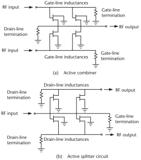
In Chapter 2 the principles behind the TWDA and the novel CSSDA are cussed. In particular, the theory and a comparison between these two types of dis-tributed amplifier architectures are presented. It is also shown how the disdis-tributed amplifier technique can be applied to other circuit functions where broadband per-formance is attractive, namely mixer, active circulator, multiplier, power combiner and splitter, impedance transformer, and oscillator.
Chapter 3 reviews the structure and the basic operation of gallium arsenide (GaAs) metal-semiconductor field effect transistor (MESFET), double-heterojunction pseudomorphic high-electron-mobility transistor (DPHEMT), and the single-heterojunction PHEMT (SPHEMT). The latter two devices are shown to be far more superior to the conventional GaAs MESFET device in terms of providing high-frequency performance with substantially improved gain, output power, and power-added efficiency.
Chapter 4 describes the procedure used for carrying out small-signal and large-signal device characterization, which is essential for obtaining accurate equivalent circuit device models of the active devices that are used for the design and modeling of the broadband amplifiers. The device’shotS-parameter data, which is obtained by biasing the devices at its nominal operating point, was used to extract the intrin-sic device elements of the small-signal model. The cold S-parameter data of the device is obtained by biasing the device at pinch-off. This data was used to derive the extrinsic device elements of the small-signal model.
To analyze the power performance of the broadband amplifier, scattering parameters alone are insufficient because under large RF drive, a transistor exhibits considerable nonlinear behavior inCgs,gm,Cgd, andRds. Hence, in order to analyze
the large-signal performance of the broadband amplifier, it was necessary to derive the device’s large-signal model from the pulsed direct current (dc)Ids–VdsandIds–Vgs
measurements. The latter measurements eliminate the dispersion effects that are shown to be very significant in the static dcIds–Vdsmeasurements.
employed is far more elegant then of the conventional numerical optimization method, which requires the small-signal model to be “fitted” to a large number of measured S-parameter data at various bias settings. One of the main problems of the latter method is the determination of the starting component values for the optimi-zation procedure. Depending on these starting values, the final values may be very different, even with low error functions, and this can result in component values that lack any physical meaning, thus leading to an inaccurate device model.
Large-signal device models are critical for accurately modeling and analyzing the broadband amplifier design for output power and power-added efficiency perform-ance. The merits of deriving the large-signal model from the device process informa-tion and the empirical method is discussed. A semiempirical method, which is a compromise between the analytical and empirical methods, is shown to provide an accurate large-signal model, as no assumptions are referenced to the physical opera-tion of the device and it uses the measured data of the device. The chapter also reviews the different methods of nonlinear analysis and large-signal modeling tech-niques. The optimum large-signal model of the devices employed was derived by “fitting” the pulsed dcIds–VdsandIds–Vgsmeasured data to the theoretically predicted
Ids–VdsandIds–Vgscharacteristics of the large-signal models available in CAD tools.
Chapter 5 provides general analyses on the different classes of amplifier opera-tion for broadband applicaopera-tions to provide an insight into how a particular class of operation may affect the amplifier’s performance in terms of power-added efficiency.
Chapter 6 describes the design, analysis, fabrication, and measured perform-ance of different types of broadband amplifiers operating across the frequency range of 2 to 18 GHz. All of the amplifiers were fabricated using hybrid MIC tech-nology. The amplifiers were fabricated on a high dielectric constant Alumina sub-strate, and all of the active devices were embedded into the circuit using chip and wire technology. The broadband amplifiers investigated include the conventional traveling wave amplifier, the feedback amplifier, novel CRTSSDAs, and a novel high-dynamic-range broadband amplifier. Finally, a novel current-sharing biasing technique is demonstrated on a feedback amplifier, which is shown to exhibit a sub-stantial improvement in efficiency and a 50% reduction in current consumption by the amplifier.
biasing of the broadband amplifiers. These coils were designed to provide low inser-tion loss and no inband resonances. Finally, the fabricainser-tion of the test carriers, amplifier housings, and test jigs are presented. The material selected for the test car-riers and amplifier housings is thermally matched to the Alumina substrate.
Chapter 8 describes the design of ultrabroadband microwave amplifiers for data modulator drivers.
Acknowledgments
The information in this book was collected over a number of years through the research and teaching activities of the authors at Filtronic Components Ltd, London Metropolitan University, and Brunel University. The authors wish to express their sincere gratitude to these organizations for making the work possible, and in par-ticular to Professor J. D. Rhodes (executive chairman of Filtronic PLC) and Dr. Keith Ferguson (managing director of Filtronic Components Ltd.) for allowing us to publish the work presented in the book. We would also like to thank Filtronic Com-ponents Ltd. for providing the facilities and funds necessary to carry out the techni-cal work; Rashid Fazaldin, who helped in the small-signal modeling process; and Steve Rackham for his help in the fabrication of all of the Alumina-based MIC amplifiers. Professor R. G. Meadows (former head of department at London Metro-politan University) is thanked for enthusiastically supporting our research activities. We would also like to thank Dr. Julie Lancashire (editorial director) and Tiina Ruonamaa of Artech House for all of their help and guidance.
Dr. Bal Virdee would like to thank his wife for her sacrifice and understanding for the very many hours of neglect during the completion of this project. Last, but not least, the authors are indebted to their families, in particular their wives Neelam, Satpal, and Najlaa, for their patience, support, and encouragement.
Overview of Broadband Amplifiers
1.1
Historical Perspective on Microwave Amplifiers
The interest in microwave techniques for communication systems has grown immensely over recent years, and the performance of microwave active and pas-sive circuits for wireless systems technology has become extremely advanced. One of the most critical active circuits employed in systems applications is the micro-wave amplifier. Because it is a highly versatile circuit function, it has always been the first to benefit from developments in the device and semiconductor technologies. Amplifiers with extremely wide bandwidths with good performance have been suc-cessfully realized in the past 2 decades in hybrid and monolithic technologies. Hence, the subject of amplifiers has been firmly established in the fields of micro-wave, optical communication, instrumentation, and EW.
It was from approximately the late nineteenth century to as early as 1930 that communication systems were severely limited due to the shortage of technology and sources for invention. During this spell, the triode electronic valve (tube) was used to develop amplifier and oscillator modules that were associated with very lim-ited applications and were mainly used for civil purposes. Many experiments were conducted for radio communication; among the experimenters was A. G. Clavier, who successfully set up a radio link across the channel between England and France in 1931 [1]. Since then, the amplifier became the arena of active research carried out by many researchers. Their primary aim was to improve the performance of its gain-bandwidth product, but this was not possible because the technology was con-strained at that time by the electronic valve.
This problem was extensively investigated by W. S. Percival [2], in 1935, who found that gain-bandwidth product is greatly affected by the capacitance and transconductance of the conventional electronic valve. In 1936, Percival elabo-rated discussion on a new type of electronic-discharge (thermionic) valve, with one or more of its electrodes made in the form of a spiral coil. This coil and the intere-lectrode capacitance form a distributed transmission system; therefore, he was the first to propose the idea of distributed amplification. This work was patented at that time in July 1936 under British Patent Number 460562. His publication states that if a system is terminated with appropriate characteristic impedance, a signal can propagate through the electrode and finally be absorbed by the termination line impedance. This discussion was then delineated on two-stage distributed
amplifiers using the thermionic valves (consisting of six screen grid vacuum tubes) [2]. The idea was based on separating the input and output capacitances of a series thermionic valve from their transconductance and thereby overcoming the problem of constraining the gain-bandwidth product associated with the earlier narrow bandwidth amplifiers. This is achieved by means of absorbing the input and output capacitances into artificial transmission lines, so that the distributed amplifier would behave as a low-pass filter with bandwidth set by the cut-off frequency of the input and output lines.
The potential of Percival’s work was not fully appreciated until a decade later, when his idea of the distributed amplifier was further investigated and developed by Ginzton [3] and Horton [4]. They managed to realize the distributed amplifier and achieved good practical results. This area of amplifier work later became highly topical for active research, resulting in more activities and discussion on the distrib-uted amplifier. Consequently, a number of publications and scientific articles appeared on different applications such as television broadcasting, radar systems, networking, and EW applications [1].
A spectacular technological maturity was established in the early 1960s by transferring the tube-valve technology to the junction transistor technology. Since then, the development of distributed amplification techniques has increased rapidly. For broadband amplifier technologies, new methods and techniques for broadband matching were established [5, 6]. Other types of amplifier designs in general also improved due to the advent of semiconductor diodes and transistors. Also different amplifiers (e.g., the varactor parametric amplifiers [7, 8], balanced transistor ampli-fier [9], traveling wave ampliampli-fier [10], and MESFET distributed ampliampli-fier [11]) could now be realized in hybrid technology.
Between 1970 and 1980, advanced GaAs FET and MESFET technologies were heavily involved in the design of hybrid microwave amplifiers and circuits [12, 13]. Later, broadband designs for preamplifiers for small signals [14, 15] and medium power amplifier for larger signals were developed [16, 17].
this is accomplished with the aid of CAD techniques [20]. In the following sections, various types of broadband amplifiers are reviewed.
1.2
Broadband Amplifiers
Broadband systems have traditionally employed TWDA, as they have been exten-sively investigated and firmly established as being reliable and robust devices that can be realized in MIC and MMIC technologies. This device has become very popu-lar due to its excellent bandwidth performance. This is possible because the input and output capacitances of the active devices are absorbed in the distributed struc-tures [21]. The resulting amplifier also exhibits very low sensitivities in process variations when realized in MMIC technology and is relatively easy to design and simulate [22].
The gain performance of a single-stage traveling wave amplifier comprising of two MESFET devices is limited to 8 to 9 dB. This is due to the gate and drain line attenuation that limits the number of FET devices in a distributed amplifier configuration. In other words, there are a certain number of devices that maximizes the gain per FET used. The limitation on the number of devices at high frequencies is mainly due to the attenuation on the gate line. The attenuation on the lines also reduces the bandwidth with an increase in the number of FETs. In practice, it is pos-sible to improve the efficiency and power output of a distributed amplifier by taper-ing the drain line impedance from section to section. Impedance tapertaper-ing forces the backward traveling current to zero at the termination, thus forcing all of the devel-oped current from each FET to propagate in the forward direction only. In order to realize high gain amplifiers, a number of the single-stage traveling wave amplifiers have to be cascaded together. The major deficiencies of the latter technique, how-ever, are those of higher manufacturing cost and a substantial reduction in the amplifier power-added efficiency (i.e., typically 7% to 14%). The improvement in efficiency demands is primarily driven by the next generation of multioctave sys-tems, such as high-data-rate fiber-optic links and EW, which require considerably lower power dissipation. Such systems have very stringent requirements from broadband amplifiers in terms of the following attributes: high stability, high gain, high output power, and high power-added efficiency. Moreover, these amplifier designs in practice are also required to meet the high production yield and repro-ducibility targets necessary to minimize manufacturing cost.
1.3
Review of Various Broadband Amplifiers
devices and novel efficiency-enhancing circuit concepts [23, 24]. In comparison with the narrowband power amplifier, the broadband power amplifier’s power-added efficiency performance is substantially lower, typically in the range of 8% to 19%. This is because the emphasis placed on the design of such amplifiers has been achiev-ing a maximum output power over the desired multioctave bandwidth, which comes at the expense of efficiency performance.
The most popular and well-established circuit techniques employed in the design of broadband amplifiers that are realized in hybrid and monolithic technologies are:
• Reactively matched circuit; • Traveling wave distributed circuit; • Feedback circuit;
• Lossy matched circuit.
The concept of cascading single-stage distributed amplifiers [25] presented in Chapters 2 and 6 has evolved to overcome the deficiencies in the TWDA’s performance.
1.3.1 Reactively Matched Amplifiers
The reactively matched amplifier, shown in Figure 1.1, is also termed as the lossless matched amplifier due to the reactively matched input and output circuits. The matching circuits are used to accomplish gain compensation (i.e., to flatten the FET’s gain roll off) by selectively creating reflections between the matching network and the active device. Because the matching networks are composed exclusively of reactive elements, the maximum gain, minimum noise figure, and maximum power output can be achieved for a given FET with a properly designed matching network. In practice, maximum gain can be achieved by optimizing the input matching cir-cuit, and the output matching circuit can be optimized to achieve maximum output power and hence power-added efficiency. The disadvantage of this type of amplifier is its relatively poor impedance match, because although the lossless matching cir-cuits provide the desired match over a narrow band of frequencies, the matching at other frequencies is degraded. This can be improved by employing isolators in the case of a single-ended design or hybrid couplers as combiners and dividers in the case of balanced amplifiers. In the single-ended case, this will result in extra cost and
RF input Inputmatching network
Output matching network
RF output FET
an increase in the overall size of the amplifier module. The balanced-amplifier approach results in an increase in output power of 3 dB; however, this comes at expense of double the dc power consumption.
Tserng, et al. [26], reported the first reactively matched 2- to 18-GHz power amplifier employing GaAs MESFET devices. The amplifier was designed using wideband impedance transformers realized in MIC, and it achieved average power-added efficiency in the range of 8% to 15% with an output power of 23 dBm. The main deficiency of this amplifier design was that the terminal voltage standing wave ratios (VSWRs) were very poor under small-signal conditions. Palmer, et al. [27], produced the first reactively matched MMIC multioctave power amplifier operat-ing over the frequency range of 6 to 18 GHz. The amplifier achieved an output power of 27 dBm with an average power-added efficiency of 19%. This was a two-stage amplifier employing a driver two-stage and an output two-stage, which had two power devices connected in a parallel configuration in order to decrease the source induc-tance and to diffuse heat concentration in the devices.
The design of amplifiers capable of high output powers require FET devices with large gate peripheries that enable high channel current densities to be achieved from the FETs. Unfortunately, a large gate width simply increases the device’s para-sitics, especially the gate-source capacitance and the gate resistance. Although it is possible to decrease the gate resistance by changing the geometry of the FET, the gate resistance of a FET usually cannot be reduced in proportion to the increase in gate width, so gain decreases as gate width increases; consequently, power FETs usually have relatively low gain. It was found that the size of the GaAs MESFETs could not be increased indefinitely because of crosstalk, phasing, and stability prob-lems. In an effort to minimize these effects, designers have developed divider/combi-ner circuits [28]. Other designs use thecluster cell matchingconcept, where input matching is achieved at the level of the individualcell clusters,which are then par-tially matched at their outputs prior to combining via quarter wavelength lines [29]. The operating bandwidth of the latter circuits is limited to an octave.
1.3.2 TWDAs
input and output resistance, thus achieving a very wide bandwidth (e.g., 2 to 18 GHz) performance. This type of amplifier eases the difficulties associated with broadband matching of the FET input and output impedances, as the input and output capacitances of the FETs are absorbed into the input gate and output drain transmission lines, respectively. The major application of this type of amplifier has been in EW, radar, and broadband communication systems, as well as in measure-ment instrumeasure-mentation. The main advantages of the amplifier are its very wide bandwidth and inherent circuit stability characteristics. The major disadvantages of the amplifier are its relatively poor output power and therefore low power-added efficiency performance, in addition to the need for multiple active devices in its implementation, which results in increased complexity and manufacturing cost.
The distributed amplifier employing solid-state GaAs MESFET devices was first investigated by Moser in 1967 [30] and by Jutzi in 1969 [31]. They realized an amplifier that used hybrid lumped element circuit technology and demonstrated its potential for providing a relatively high gain bandwidth product. In 1982, the first 1- to 13-GHz monolithic traveling wave amplifier was presented by Ayasli, et al. [32]. In the following year a practical design approach for both lumped element and transmission line element traveling wave amplifiers was formalized by Niclas, et al. [33]. It was later that the expressions for the gain and bandwidth of the distributed amplifier in terms of the input and output propagation constant and the cut-off fre-quency were developed by Beyer, et al. [34].
Ayasli, et al. [22], reported 2- to 20-GHz decade band amplification with 30-dB gain with GaAs FETs in monolithic form. He also investigated the power-limiting mechanisms in a GaAs FET traveling wave amplifier and described a circuit approach that decreases the effect of some of these limiting mechanisms [21]. He basically used two traveling wave amplifiers that had a common drain line. The input power was split into the two gate lines, each employing four 150-µm FETs, using a Wilkinson divider. The FETs excited from the two gate lines are combined on the single drain line, effectively giving four 300-µm drain periphery. Thus, the total gate periphery is doubled without affecting the loading on the gate lines. Also, the load line impedance is halved, as there is twice the drain periphery on the output
L/2
Zo
L/2
L/2 L L L/2
L L
Lbias Cbias
Lbias
Cbias
Zo
line. Because gain per stage is not significantly affected, the efficiency of the ampli-fier is effectively doubled. This ampliampli-fier produced 0.25W of output power across 2 to 20 GHz with power added-efficiencies in the range of 7% to 14%.
Kim and Tserng [35] described a novel concept of reducing the gate line losses by using series capacitors with the GaAs MESFET devices. Their concept was to increase the gate periphery of the GaAs MESFET devices, resulting in an increased broadband output power performance. An output power of 0.5W was achieved with 4-dB small-signal gain over 2- to 21-GHz bandwidth. The average power-added efficiency achieved across the bandwidth was approximately 7%.
Prasad, et al. [36], described the quantitative procedures for the design of GaAs MESFET distributed amplifiers using series capacitors in the device gate circuits. They showed that the choice of series capacitors allows the designer to trade gain for bandwidth while maintaining a given gain-bandwidth product. It was also shown that the input power capability could be increased by the use of series capaci-tors when the device pinch-off is the power-limiting factor. Furthermore, they also showed how the addition of series capacitors enables the gate periphery of an ampli-fier to be increased, which results in an increase in power-bandwidth product. Ayasli, et al. [37], followed a similar concept where theycapacitively coupledthe individual GaAs MESFETs to the gate input line through discrete series capacitors. One watt of output power was achieved over 2 to 8 GHz with power-added effi-ciency in the range of 5% to 7%.
Paoloni, et al. [38], describe an innovative topology of a distributed ampli-fier based on input and output broadband Lange couplers. The modified oper-tion mechanism of the new configuraoper-tion, in comparison with the convenoper-tional distributed amplifier, establishes a remarkable improvement of the output power, power-added efficiency, and small-signal gain. The performance of a 2- to 18-GHz conventional distributed amplifier is presented with power-added efficiency in the range of 8% to 15%. The newly configured amplifier design achieves power-added efficiency in the range of 13% to 19%, which is a significant improvement when compared with the conventional distributed amplifier case.
Aitchison, et al. [40, 41], proposed a novel amplifier based on the TWDA, which they referred to as a dual-fed distributed amplifier. This was because the input signal is fed to both ends of the gate line by means of a hybrid coupler. In addition, because superposition applies, the benefit of gain is obtained in both directions. Both ampli-fied signals are collected by means of a second hybrid, as illustrated in Figure 1.3. The use of a 90° hybrid results in forward and reverse gain benefit being obtained at the output port so that there is a 6-dB increase in gain above that obtained from the same amplifier circuit used unidirectionally. This benefit is obtained up to at least half of the cut-off frequency. Thus, 6 dB of gain is obtained from only two FETs. In addition, the input power for 1-dB compression is increased by 3 dB, and hence the 1-dB gain compression power is 3 dB higher than for the corresponding unidirectional ampli-fier. Measurements also show that a carrier to third-order intermodulation product ratio (C/I) of 25 dB can be achieved with an input power back off of 9 dB for conven-tional power distributed amplifier, while the corresponding figure for the dual-fed distributed amplifier is 6 dB, an improvement of 3 dB. There is also a noise figure improvement of about 2 dB, which diminishes with increase in frequency.
More recently ultrabroadband traveling wave amplifiers operating at up to 180 GHz have been realized by Agarwal, et al. [42]. This amplifier exhibited a gain of 5 dB across the 180-GHz bandwidth. Agarwal and his team also reported traveling wave amplifiers having 1- to 112-GHz bandwidth with 7-dB gain, and 1- to 157-GHz bandwidth with 5-dB gain. All of these amplifiers were fabricated using a 0.1-µm gate length InGaAs/InAlAs HEMT MMIC technology.
1.3.3 Broadband Feedback and Lossy Matched Amplifiers
The amplification of microwave signals employing amplifiers, which only require a single device to achieve the multioctave bandwidth, was proposed by Niclas, et al.
L/2
L/2 L L/2
L L/2
90° Hybrid
90° Hybrid
Input Output
[43, 44]. These amplifiers are defined as thefeedbackandlossy matched. The feed-back amplifier, shown in Figure 1.4, employs shunt feedfeed-back between the gate and drain of the active device used in the circuit. The major advantages of the feedback amplifier are:
• The circuit is less complex compared with the reactively matched and
travel-ing wave amplifier circuits and therefore is easier to realize.
• The amplifier can provide higher power-added efficiency performance when
compared with the conventional traveling wave amplifiers.
• The amplifier offers a cost-effective multioctave bandwidth amplifier design. • It has excellent performance in achieving flat gain and unconditional stability,
and it provides very good input and output match.
• The amplifier can be realized in hybrid MIC and MMIC circuit technologies. • It provides lower distortion and sensitivity to active device variations.
The main disadvantage of this type of amplifier is the erosion of the its output power and noise figure over the lower end of the frequency band due to loss associ-ated with the feedback resistor.
The feedback path consists of three elements (i.e., resistorRfb, inductorLfb, and
the capacitorCfb). The value of the feedback resistorRfbcontrols the gain and
band-width of the amplifier. The gate inductanceLg, the drain inductance Ld, and the
feedback inductanceLfbcan be optimized to extend the amplifier’s bandwidth [43].
The feedback inductanceLfbreduces the effectiveness of the negative feedback with
increasing frequency. The drain inductance Ld is selected to compensate for the
intrinsic drain-source capacitance of the device up to the cut-off frequency. The dc block capacitorCfbis used to isolate the gate from the drain bias supply. The
capaci-torCfband bias inductorsL1andL2also determine the amplifier’s bandwidth
per-formance, which has to be resonance free across the desired bandwidth. The feedback amplifier can be very sensitive to frequency when implemented in hybrid technology; hence, its implementation dominates in MMIC technology.
Lfb Rfb
Ld
L2
RF output RF input
L1
Lg Cfb
The lossy matched amplifier employs resistorsR1andR2at the input and output matching circuits, respectively, as illustrated in Figure 1.5. These resistors are used to provide gain equalization (i.e., flat gain response) by introducing high attenuation at low frequencies and low attenuation at high frequencies, while maintaining a good input and output match over the desired broad bandwidth. This fact makes the amplifier suitable for cascading without the need for isolators to improve interstage matching, as is the case for the reactively matched amplifier. Therefore, they are rela-tively smaller and have lower power consumption. The amplifiers provide broad bandwidth performance at the expense of low gain, low output power, high noise fig-ure, and poor power-added efficiency [43]. This is mainly due to losses in the resis-tors, which are used in the input/output matching and interstage networks.
1.3.4 CSSDAs
Although the TWDA has the desirable attributes of flat gain and good terminal match over a wide frequency range, it is deficient in terms of gain and output power, and it requires multiple devices leading to a relatively large gain module. These drawbacks stimulated work for improving the design of conventional distributed amplifiers in terms of realizing a more compact circuit using fewer devices to produce high levels of gain. Minnis [45] described for the first time the principles of cascadable amplifiers. His simulation results indicate that the single-stage distrib-uted amplifier employing 800-µm FET is capable of delivering a 6-dB gain over 7 to 14 GHz and occupies less than 1 mm2
of GaAs. Later in the same year, Moazzam and Aitchison [40] described a single-stage distributed amplifier that is based on the dual-fed distributed amplifier. Figure 1.6 illustrates this amplifier. In this configuration, the input and output line idle ports are reactively terminated, which results in a significant improvement in gain and power-added efficiency over that available from a conventional TWDA and dual-fed distributed amplifier. The signal at the input port travels down the gate line and is reflected at the open circuit so that the gate voltage is double the input voltage. Similarly, the output current in the drain line load is due to current reflected from the drain open circuit as well as the direct drain current. Moazzam and Aitchison theoretically analyzed this configuration, and their simulation results show that the single-stage distributed amplifier with open-circuited terminations have a relative flat gain response of 9.5 dB up to 5 GHz beyond which it gradually diminishes. The gain response is approximately the same up to 5 GHz for a four-stage conventional distributed amplifier. The power-added
R2
RF output FET
RF input
R1
efficiency of the single-stage distributed amplifier is more than quadrupled in comparison with that of the four-stage distributed amplifier. But, using short-circuited terminations in the single-stage distributed amplifier results in a bandpass-like gain response with a maximum gain occurring at its center. This gain response can be shifted from one end of the band to the other by changing the phase of the reflecting terminations (e.g., by terminating the idle ports with inductors or capacitors). The drawback of the single-stage distributed amplifier is its poor input and output match, and its 3-dB bandwidth is approximately half that of a conven-tional distributed amplifier.
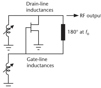
Figure 1.7 shows how the single-stage distributed amplifier, with some modifi-cation, can be used as a tunable oscillator [40]. The output of the amplifier is con-nected to the input through a length of line to provide an appropriate phase change of 180° at the required frequency of oscillation. The frequency of oscillation is tun-able over a broad bandwidth by means of adjusting the terminating reactances.
RF output Drain-line
inductances
Gate-line inductances
180° atfo
Figure 1.7 Single-ended dual-fed distributed amplifier used as a tunable oscillator.
RF output
RF input
Es OC/SC
OC/SC
Drain-line inductances
Gate-line inductances OC = open circuit
SC = short circuit
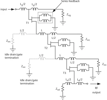
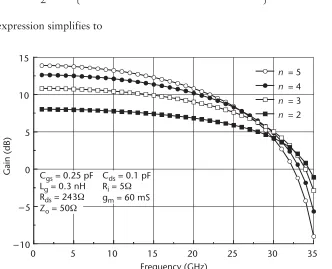
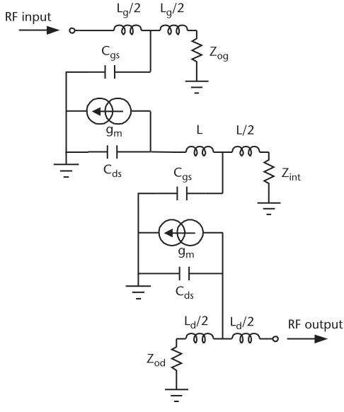
Liang and Aitchison [46] extended the concept of a single-stage distributed amplifier by transforming the configuration into a cascade ofnsingle-stage distrib-uted amplifiers (n-stage CSSDA), wherenis the number of devices, as is illustrated in Figure 1.8. In this configuration, the idle drain/gate termination is omitted for stages other than the first and last. With no idle drain/gate termination, the voltage swing across the input gate of the active device is increased, which consequently enhances the amplifier’s gain. A series feedback is included in the amplifier configu-ration as an external inductance added to the source terminal of the FET at each stage. In this configuration, the input signal power is coupled and amplified via the transconductance of the FETs, and it emerges from the drain line. The simulation results of this amplifier show that a cascade of four single-stage distributed amplifi-ers provides a 20-dB flat gain performance and return loss better than 14 dB. The conventional four-stage distributed amplifier configuration employing the same FETs provides a gain of 9 dB over the same bandwidth. This clearly shows the superiority of the cascaded single-stage distributed amplifier over the conventional distributed amplifier.
RF input
L /2g L /2g
Zog Series feedback
L/2 L
L/2 Z
int
T1
T2
T3 Idle drain/gate
termination L/2 L
L/2
Zint
Idle drain/gate termination
Zod
L /2d L /2d
RF output Zint
Zint
The CSSDA design proposed by Liang and Aitchison [46] is difficult to realize in practice because:
• The series feedback is difficult to realize, especially in hybrid form using
pack-aged active devices.
• The series feedback is very sensitive at high frequency and may drive the
amplifier into oscillation (instability) at some stage across the wide bandwidth.
• The design requires transistors with high transconductance greater than
50 mS to compensate for losses caused by the series feedback.
Despite these shortcomings, the series feedback can be a useful technique for modifying the input impedance (usually increasing it) or in some cases for improv-ing the noise figure.
Stability can be more of an issue with the CSSDA configuration than in an ordi-nary distributed amplifier, other than due to the series feedback element. This is because the high gain associated with the cascaded distributed amplifier may result in excessive coupling between the input and output ports, which can lead to instabil-ity. Coupling between the input and output of the individual cascaded devices may also erode the amplifier’s stability. Hence, in the CSSDA design, careful considera-tion must be exercised in order to ensure stable operaconsidera-tion over its frequency band-width.
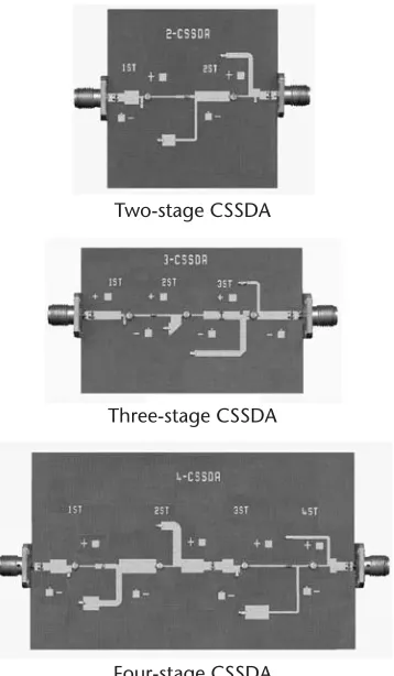
Banyamin, et al. [47], improved the single-stage distributed amplifier circuit by eliminating the series feedback network and its detrimental effect of eroding the gain potential of the amplifier. Banyamin realized the amplifier in two-, three-, and four-cascaded single-stage distributed amplifier using packaged heterojunction FET devices and showed that the new CSSDA amplifier provides useful gain response over a bandwidth of 2 to 10 GHz as well as providing stable operation. The com-parison between the CSSDA with the conventional traveling wave amplifier realized using the same active devices is given in Table 1.1. It can be seen that a four-stage CSSDA provides a gain of 37 dB, compared with 10 dB obtained from the conven-tional traveling wave amplifier realized using the same devices achieved across the same bandwidth [48]. The prototypes of the amplifier are shown in Figure 1.9.
The CSSDA configuration is discussed further in Chapter 2.
Table 1.1 Measured Performance of the CSSDA
CSSDA Number of Stages Available Power Gain (dB) Return Loss (dB)
2 20 >10
3 30 >10
4 37 >10
TWDA Number of Stages Available Power Gain (dB) Return Loss (dB)
2 6 >10
3 10 >10
References
[1] Seeger, J. A., Microwave Theory, Components, and Devices, Englewood Cliffs, NJ: Prentice-Hall, 1986.
[2] Percival, W. S.,Improvement in and Relating to Thermionic Valve Circuits, British Patent 460562, January 1937.
[3] Ginzton, E. L., et al., “Distributed Amplification,” Proc. I.R.E., Vol. 36, 1948, pp. 956–969.
[4] Horton, W. H., J. H. Jasberg, and J. D. Noe, “Distributed Amplifiers: Practical Considera-tion and Experience Results,”Proc. I.R.E., Vol. 38, 1950, pp. 748–753.
[5] Williams, E.,Electrical Filter Circuits—An Introduction Course, London: Sir Isaac Pitman and Sons Ltd, 1963.
[6] Youla, D. C., “A New Theory of Broad-Band Matching,”IEEE Transaction on Circuit Theory, March 1964, pp. 30–50.
[7] Walter, H. K., “A Broad-Band Theory for Varactor Parametric Amplifiers—Part I,”IEEE Transaction on Circuit Theory, August 1964, pp. 50–58.
[8] Walter, H. K., “A Broad-Band Theory for Varactor Parametric Amplifiers—Part II,”IEEE Transaction on Circuit Theory, November 1964, pp. 59–66.
Two-stage CSSDA
Three-stage CSSDA
Four-stage CSSDA
[9] Engelbrecht, R. S., and K. Kurkawa, “A Wide-Band Low Noise L-Band Balanced Transis-tor Amplifier,”Proc. IEEE, March 1965, pp. 237–247.
[10] Mclver, G. W., “A Traveling Wave Transistor,”Proc. IEEE (Letter), Vol. 53, November 1965, pp. 1747–1748.
[11] Jutzi, W., “A MESFET Distributed Amplifier with 2 GHz Bandwidth,”Proc. IEEE, Vol. 57, 1969, pp. 1195–1196.
[12] Pengelly, R. S., “Broadband Lumped-Element X-Band GaAs FET Amplifier,”Electronics Letters, February 1975, pp. 58–60.
[13] Vendelin, G. D., and M. Omori, “Circuit Model for the GaAs MESFET Valid to 12 GHz,”
Electronics Letters, February 1975, pp. 60–61.
[14] Slaymarker, N. A., R. A. Soares, and J. A. Turner, “GaAs MESFET Small Signal X-Band Amplifiers,” IEEE Transaction on Microwave Theory and Techniques, Vol. MTT-24, No. 6, June 1976, pp. 329–337.
[15] Nowak, M. M., P. A. Terzian, and R. D. Fairman, “K-Band FET Amplifiers,”Electronics Letters, March 1977, pp. 159–160.
[16] Hornbuckle, D. P., and L. J. Kuhlman, “Broad-Band Medium-Power Amplification in the 2-12.4 GHz Range with GaAs MESFET’s,”IEEE Transaction on Microwave Theory and Techniques, Vol. MTT-24, No. 6, June 1976, pp. 338–350.
[17] Niclas, K. B., et al., “A 2-12 GHz Medium-Power GaAs MESFET Amplifier,”IEEE Jour-nal Soild-State Circuits, Vol. SC-13, No. 4, August 1978, pp. 520–527.
[18] Archer, J. A., F. A. Petz, and H. P. Weidlich, “GaAs FET Distributed Amplifier,” Electron-ics Letters, June 1981, pp. 433–434.
[19] Ayasli, Y., et al., “Monolithic Traveling-Wave Amplifier,”Electronics Letters, June 1981, pp. 413–414.
[20] Pucel, R. A., “Design Consideration for Monolithic Microwave Circuits,”IEEE Transac-tion on Microwave Theory and Techniques, Vol. MTT-29, No. 6, June 1981, pp. 513–534. [21] Ayasli, Y., et al., “2 To 20 GHz GaAs Traveling Wave Power Amplifier,”IEEE Trans. on
Microwave Theory and Techniques, Vol. 32, No. 3, 1984, pp. 290–295.
[22] Ayasli, Y., et al., “2 To 20 GHz GaAs Traveling Wave Amplifier,”IEEE Trans. on Micro-wave Theory and Techniques, Vol. 32, No. 1, 1984, pp. 71–77.
[23] Khatibzadeh, M. A., and H. Q. Tserng, “Harmonic Tuning of Power FETs at X-Band,”
IEEE MTT-S Digest, 1990, pp. 989–992.
[24] Ingruber, B., W. Pritzl, and G. Mageri, “High Efficiency Harmonic Control Amplifier,”
IEEE MTT-S Digest, 1996, pp. 859–862.
[25] Aitchison, C. S., and Y. J Liang, “A Proposal for Broadband High Gain Block Using Cas-caded Single Stage Distributed Amplifiers,”IEEE EDMOt, 1995, pp. 173–178.
[26] Tserng, H.Q., et al., “2- to 18-GHz High Efficiency Medium Power GaAs FET Amplifiers,”
IEEE MTT-S Digest, 1981, pp. 31–33.
[27] Palmer, C. D., P. Saunier, and R.E Williams, “A GaAs Monolithic 6- to 18-GHz Medium Power Amplifier,”IEEE Trans. on Microwave and Millimeter Wave Monolithic Circuits Symposium Digest, 1984, pp. 57–57.
[28] Schellenberg, J. M., and H. Yamasaki, “A New Approach to FET Power Amplifiers,”
Microwave Journal, 1982, pp. 51–66.
[29] Degenford, D., et al., “Broadband MMIC Power Amplifier Development,” Microwave Journal, 1982, pp. 89–96.
[30] Moser, “140 MHz Kettenverstarker Mit Feldeffekttransistoren,”Inter. Elek Rundschau,
Vol. 5, 1967, pp. 109–115.
[31] Jutzi, W., “A MESFET Distributed Amplifier with 2 GHz Bandwidth,” Proc. IEEE,
[32] Ayasli, Y., et al., “A Monolithic GaAs 1 To 13 GHz Traveling Wave Amplifier,”IEEE Trans. on Microwave Theory and Techniques, Vol. 30, No. 7, 1982, pp. 976–980. [33] Niclas, K. B., et al., “On Theory and Performance of Solid State Microwave Distributed
Amplifiers,”IEEE Trans. on Microwave Theory and Techniques, Vol. 31, No. 6, 1983, pp. 447–456.
[34] Beyer, J. B., et al., “MESFET Distributed Amplifier Guidelines,”IEEE Trans. on Micro-wave Theory and Techniques, Vol. 32, No. 3, 1984, pp. 268–275.
[35] Kim, B., and H. Q. Tserng, “0.5W, 2 To 21 GHz Monolithic GaAs Distributed Amplifier,”
Electronic Letters,Vol. 20, No. 7, 1984, pp. 228–289.
[36] Prasad, S. N., J. B. Beyer, and I. S. Chang, “Power-Bandwidth Considerations in the Design of MESFET Distributed Amplifier,”IEEE Trans. on Microwave Theory and Techniques, Vol. 36, No. 7, 1988, pp. 1117–1123.
[37] Ayasli, Y., et al., “Capacitively Coupled Traveling Wave Power Amplifier,”IEEE Trans. on Microwave Theory and Techniques, Vol. 32, No. 12, 1984, pp. 1704–1709.
[38] Paoloni, C., and S. D’Agostino, “Design of High-Performance Power-Distributed Amplifier Using Lange Couplers,” IEEE Trans. on Microwave Theory and Techniques, Vol. 42, No. 12, 1994, pp. 2525–2530.
[39] Shapiro, E. S., et al., “A High-Efficiency Traveling Wave Power Amplifier Topology Using Improved Power-Combining Techniques,”IEEE Trans. on Microwave and Guided Wave Letters, Vol. 8, No. 3, 1998, pp. 133–135.
[40] Moazzam, M. R., and C. S. Aitchison, “A High Gain Dual-Fed Single Stage Distributed Amplifier,”IEEE MTT-S Digest, 1994, pp. 1409–1412.
[41] Aitchison, C. S., et al., “The Dual-Fed Distributed Amplifier,”IEEE MTT-S Digest, 1988, pp. 911–914.
[42] Agarwal, B., et al., “112 GHz, 157 GHz, and 180 GHz InP HEMT Traveling-Wave Ampli-fiers,”IEEE Trans. On Microwave Theory and Techniques, Vol. 46, No. 12, December 1998, pp. 2553–2559.
[43] Niclas, K. B., et al., “The Matched Feedback Amplifier: Ultrawideband Microwave Amplifi-cation with GaAs MESFETs,”IEEE Trans. on Microwave Theory and Techniques, Vol. 28, No. 4, 1980, pp. 285–294.
[44] Niclas, K. B., “Reflective Match, Lossy Match, Feedback and Distributed Amplifiers: A Comparison of Multioctave Performance Characteristics,” IEEE, MTT-S Symposium Digest, 1984, pp. 215–220.
[45] Minnis, B. J., “The Traveling Wave Matching Technique For Cascadable MMIC Amplifi-ers,” IEEE Trans. on Microwave Theory and Techniques, Vol. 42, No. 4, 1994, pp. 690–692.
[46] Liang, J. Y., and C. S. Aitchison, “Gain Performance of Cascade of Single Stage Distributed Amplifiers,”Electronics Letters, Vol. 31, No. 15, July 1995, pp. 1260–1261.
[47] Banyamin, B., et al., “A New High Gain Broadband Amplifier Using Cascaded Single Stage Distributed Amplifiers,”Asia-Pacific Microwave Conference, 1998, pp. 753–756. [48] Banyamin, B., and M. Berwick, “The Gain Advantages of Four Cascaded Single Stage
Principles and Applications of Distributed
Amplifiers
2.1
Introduction
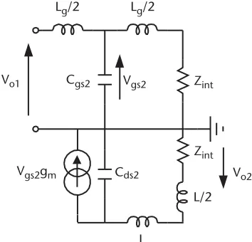
This chapter describes the principles behind the conventional TWDA and the CSSDA. A lossless cascade of two single-stage distributed amplifier (two-stage CSSDA) design using a simplified unilateral FET model is investigated. The effect of the interstage characteristic impedance on the available power gain and the influ-ence of intrinsic FET elements on the CSSDA performance are analyzed. A compari-son is provided between the conventional TWDA and CSSDA designed using identical devices. Finally, it is shown that the distributed amplifier is not only appli-cable to wideband multioctave amplifiers, it can also be applied to other circuit functions where broadband performance is needed.
2.2
Heterojunction Field Effect Transistor
The active device employed in the design and analysis of the CSSDA presented in this chapter is the heterojunction field-effect transistor (HJ-FET) (NE32584C) [1]. The choice of this device was made arbitrarily; however, it has an excellent low noise of 0.45 to 0.55 dB and high associated gain of 12.5 dB at 12 GHz. Its simpli-fied unilateral equivalent circuit is shown in Figure 2.1. The gate and drain
17
Gate Drain
Source Cgs
Ri
Vgs
Cgd
g Vm gs R
ds Cds
Iin Io
channels have parasitic reactance Cgs and Cds, respectively. The feedback capaci-tance Cgd represented by the dotted line is usually ignored in the simplified device model. The transconductancegmis a voltage-controlled current source that governs the magnitude of the current flowing through the device. The trans-conductance is controlled by the voltage swing Vgs across the FET’s input gate capacitanceCgs.
In reality, the FET’s small-signal equivalent circuit is complicated, as illustrated in Figure 2.2. The elements enclosed by the dotted line box are referred to as the intrinsic elements. The remaining parts are referred to as extrinsic elements or para-sitic elements, where resistorsRg, Rd, andRsrepresent the bond-wire resistances at
the gate, drain, and source terminals, respectively. The inductorsLg,Ld, andLsare
bond-wire inductances at the gate, drain, and source terminals, respectively. The feedback capacitance Cgd is responsible for reverse gain or isolation, S12. This
capacitance is used to differentiate whether the device is classified as unilateral or nonunilateral. A FET with a high value ofCgdis nonunilateral, while one with low
Cgd is unilateral. The isolation S12 of this HJ-FET is very small (typically, its
magnitude varies between 0.025 to 0.098 dB across 2 to 18 GHz). Therefore, it is assumed to be unilateral. This implies that the transistor die has a negligible internal feedback. Packaged HJ-FETs normally have associated external parasitic capacitances caused by the packaging of the device. These capacitances are repre-sented by Cgdp that exists between the gate and drain channels, Cgsp that exists
between the gate and source channels, andCdsp that exists between the drain and
source channels. Their values are relatively small and depend entirely on the pack-aging type.
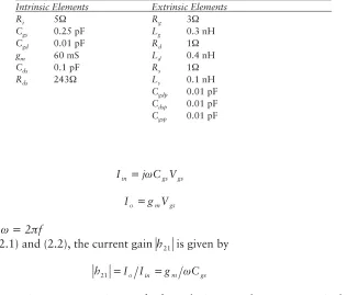
The element values in the small-signal equivalent circuit model for this HJ-FET were obtained using a commercial simulation tool and are given in Table 2.1.
Considering the circuit diagram in Figure 2.1, the inputIinand outputIocurrents
are given by
Gate Drain
Source Cgs
Ri
Vgs
Cgd
g Vm gs Rds Cds
Rg Lg Ld Rd
Ls
Rs Cgdp
Cgsp Cdsp
Iin = ωj C Vgs gs (2.1)
Io =g Vm gs (2.2)
where ω =2πf
From (2.1) and (2.2), the current gainh21 is given by
h21 =Io Iin =gm ωCgs (2.3)
The maximum power gain transfer from the input to the output terminal of the transistor is given by [2]
Maximum power gain=
= I
I R
R f
f R
R
o
in ds
i
t ds
i
2 2
4 4 (2.4)
whereftis the maximum cut-off frequency.
The maximum cut-off frequency (i.e., the frequency at which the short-circuit current gain of the transistor drops to unity) is defined as the gain-bandwidth prod-uct, which can be obtained from (2.3) and is given by
ft =gm 2πCgs (2.5)
The maximum frequency of oscillation fmax (i.e., the frequency at which the
available gain power of the transistor is unity) is obtained from (2.4) and is represented by
f f R R
t ds
i
max =2 (2.6)
From the small-signal equivalent circuit element values given in Table 2.1,ftand
fmaxof the HJ-FET are found to be 38.2 GHz and 133 GHz, respectively.
Table 2.1 Equivalent Circuit Parameters of the HJ-FET (NE32584C)
Intrinsic Elements Extrinsic Elements
Ri 5Ω Rg 3Ω
Cgs 0.25 pF Lg 0.3 nH
Cgd 0.01 pF Rd 1Ω
gm 60 mS Ld 0.4 nH
Cds 0.1 pF Rs 1Ω
Rds 243Ω Ls 0.1 nH
Cgdp 0.01 pF
Cdsp 0.01 pF
2.3
Conventional TWDA
As mentioned in Chapter 1, the TWDA is associated with two artificial transmission lines, one that makes up the input gate line and another that forms the drain output line. The artificial lines basically consist of a ladder network of series inductance and shunt capacitances, hence the formation of two constant-ktransmission lines that have different cut-off frequencies and attenuation characteristics. The shunt capaci-tors of the gate line are supplied by the gate capacitanceCgsof the FETs, whereas the drain-line shunt capacitors are supplied by the FET’s drain capacitanceCds. Lengths of transmission line are used to form the series inductances. Figure 2.3 shows the cir-cuit diagram of the TWDA, in which four identical active devices are connected in parallel. Each stage can be considered a T-section network connected in parallel. The purpose of the artificial transmission lines is to effectively remove the gate and drain capacitances associated with the active device by absorbing them within an artificial line. Such an ideal artificial line has the property that power can be propa-gated along the line from a matched generator to a matched load up to the cut-off frequency of the line, at which point propagation ceases and all power is reflected. In practice, the cut-off frequency is limited by the gate capacitance of the FET and the gate-line inductance.
In the distributed amplifier, the input signal propagates down the gate line, with each FET tapping off some of the input signal. The input voltage that appears at the gate of each FET is amplified via the FET’s transconductance, producing current in the drain line. For the distributed amplifier to produce useful gain, it is essential that these drain currents add in phase as the signal propagates along the drain line toward the amplifier’s output. This means that the phase shift between FETs along the drain line must be exactly the same as the phase shift between FETs along the gate line. This is achieved by carefully choosing the propagation constants and lengths of the gate and drain lines for constructive phasing of the output signals. The termination impedances on the lines serve to absorb waves traveling in the reverse directions. Unfortunately, as the artificial lines are heavily loaded by the FET’s
RF output
Gate-line termination Drain-line inductances
Gate-line inductances
FETs
RF input
resistances, the number of active device sections cannot be added indefinitely. This is because the attenuation along the transmission lines will eventually exceed the gain obtained by adding an additional active device.
2.3.1 Available Gain of a TWDA
The forward gain of a traveling wave amplifier comprised ofnactive devices can be derived by using the simple amplifier model of Figure 2.4. Essentially, the FET is considered to be loss free and to consist of a gate capacitanceCgsand a drain current generatorInwith associated drain capacitanceCds. Other elements in the more gen-eral equivalent circuit are neglected to simplify the analysis presented here. Simi-larly, the artificial transmission lines, which form the input gate-line inductanceLg and the output drain-line inductance Ld, are considered to be loss-free lumped components. The gate and drain lines are terminated in their characteristic imped-ances Zg and Zd, respectively. It is assumed that the external source and load impedancesZgandZdare purely real (i.e., 50Ω).
In the amplifier circuit, a wave from the gate generator propagates down the gate line with a phase constant βgper section and is dissipated entirely in the right-hand gate load. The voltage across each input gate capacitor Cgs causes the
corresponding current generator to produce currentgmVgsin the drain line, which
flows in both directions with a phase constant ofβd per section. Thus, the power
will be dissipated in both of the drain loads. Hence, we need to consider the forward gain to the right-hand drain load and the reverse gain to the left-hand drain load.
The expression for the forward small-signal available gain can be obtained by considering that the FET current generators have a magnitudeI1,I2…,In. Then the
total currentId in the loadZdis the superposition of the drain line currents given
by [3]
( )
{
}
Id =1 I el −jn d +I e−j n− d I en −jnd
2 2
1
β β , , β
K (2.7)
Zg Es
Zd
Lg Lg Lg Lg
Ld Ld Ld Ld
Cgs Cgs Cgs Cgs Zg
Zd
Cds I1 Cds I2 Cds I3 Cds In
First stage Second stage n stage
The voltage wave propagating down the gate line due toEsproduces voltages
V1,V2,…,Vnacross each input gate capacitor. If the voltage across the input
termi-nal of the amplifier isVin, then
V V ein j g V V ein j g Vn V ein nj g
1 2
2
= −β , = − β ,..., = − β (2.8)
Now
I1 =g Vm 1, I2 =g Vm 2,..., In=g Vm n (2.9)
Because we have assumed the gate line to be loss free, the following applies
V1 =V2 =Vn =Vin (2.10)
and
I1 =I2 =In =Iin (2.11)
Therefore,
( ) (( ) ) ( )
Id V gin m e j n d g e j n d g e j d n g
= + + + − + − − + − + 1 2 1 2 β β β β β β ... ∆ (2.12)
This expression simplifies to
( )
( )
I V g e
e
e
d in m
j n j j n d g d g = − − − + − − − + 1 2 1 1 1 1 β β β β β ∆
( d+ βg)
(2.13)
However,Vinis equal toEs/2 for a matched line, so (2.13) can be written as
(
)
(
)
I E g n
d s m
d g d g = − − 1 4 2 1 2 sin sin β β β β (2.14)
The power dissipated in the loadZdis therefore given by
(
)
(
)
E g n Z s m d g d g d 2 2 2 16 2 1 2 sin sin β β β β − − (2.15)E Z s d 2 4 (2.16)
The forward available gain is given by
(
)
(
)
G g Z Z
n
twa
m d g d g
d g = − − 2 2 4 2 1 2 sin sin β β β β (2.17)
The function in the braces can be simplified in the limiting case asβg→ βd. The
sine function can be represented by the following series:
sin
! ! ...
x= −x x +x −
3 5
3 5 (2.18)
so
(
)
(
)
(
)
lim sin sin β β β β β β β d g d g d g d n n − → − − = 0 2 1 2 2 2(
)
(
)
(
)
(
)
− − − + − − − + β β β β β β βg d g
d g d g
n 2 3 1 2 1 2 3 3 3 ! ... ! .
(
)
(
)
..lim ! ...
= − → − − × + − 2 3 2
0 4 3
1 β β β β β d g d g d n n
(
−)
× + = βg n 2 2 24 3! ...
Then the forward available gain can be represented by this simplified expression
Gtwa =14n g Z Z2 m2 d g (2.19)
This expression is significant in that it is frequency independent up to the cut-off frequency of the artificial transmission line. The cut-cut-off frequency of the two transmission lines can be altered by the appropriate selection ofβdandβg. It
indi-cates that the gain can be increased without limit by simply increasingn while maintaining a constant bandwidth; however, this only applies in an ideal loss-free case.
In practice, the gain of the amplifier does not increase monotonically with n because of losses in the gate and drain lines. A more accurate gain expression is given by [4, 5]
G g Z Z e e
A A
twa m d g
A n A n
where
Agis the gate-line attenuation Adis the drain-line attenuation
The optimum number of devicesNoptthat maximizes gain at a given frequency is
given by the expression [6]
N A A A A opt d g d g = − ln (2.21)
The expressions for the gate- and drain-line attenuation factors are derived from the propagation function for a constantkline and are given by
Ag c g c c g = − − ω ω ω ω ω ω 2 2
1 1
ω ωc 2 (2.22) Ad d c c = − ω ω ω ω 1 2 (2.23) where
ωis the midband radian frequency ωcis the radian cut-off frequency
ωg
i gs
R C
= 1 (2.24)
ωd
ds ds
R C
= 1 (2.25)
ωc
g gs d ds
L C L C
= 2 = 2 (2.26)
substantially larger attenuation factor than the drain line and has a lower cut-off frequency. The gain performance is also limited by the gate-line attenuation factor because the gate-line attenuation will eventually exceed the added gain obtained by increasing the number of amplifier sections. The former constraints usually limit the gain and bandwidth attainable with practical realizations.
The effect of the number of amplifier stages on the gain and bandwidth for a typical FET distributed amplifier is shown in Figure 2.5. This analysis shows improvement in gain as the number of amplifier stages is increased; however, the gain increas