Ultra Wideband
Series Editor: Anantha Chandrakasan
Massachusetts Institute of Technology Cambridge, Massachusetts
Ultra Wideband: Circuits, Transceivers, and Systems Ranjit Gharpurey and Peter Kinget (Eds.)
ISBN 978-0-387-37238-9, 2008
mm-Wave Silicon Technology: 60 GHz and Beyond Ali M. Niknejad and Hossein Hashemi (Eds.) ISBN 978-0-387-76558-7, 2008
Creating Assertion-Based IP Harry D. Foster and Adam C. Krolnik ISBN 978-0-387-36641-8, 2007
Design for Manufacturability and Statistical Design: A Constructive Approach Michael Orshansky, Sani R. Nassif, and Duane Boning
ISBN 978-0-387-30928-6, 2008
Low Power Methodology Manual: For System-on-Chip Design
Michael Keating, David Flynn, Rob Aitken, Alan Gibbons, and Kaijian Shi ISBN 978-0-387-71818-7, 2007
Modern Circuit Placement: Best Practices and Results Gi-Joon Nam and Jason Cong
ISBN 978-0-387-36837-5, 2007 CMOS Biotechnology
Hakho Lee, Donhee Ham and Robert M. Westervelt ISBN 978-0-387-36836-8, 2007
SAT-Based Scalable Formal Verification Solutions Malay Ganai and Aarti Gupta
ISBN 978-0-387-69166-4, 2007 Ultra-Low Voltage Nano-Scale Memories Kiyoo Itoh, Masashi Horiguchi and Hitoshi Tanaka ISBN 978-0-387-33398-4, 2007
Routing Congestion in VLSI Circuits: Estimation and Optimization Prashant Saxena, Rupesh S. Shelar, Sachin Sapatnekar
ISBN 978-0-387-30037-5, 2007
Ultra-Low Power Wireless Technologies for Sensor Networks Brian Otis and Jan Rabaey
ISBN 978-0-387-30930-9, 2007
Sub-Threshold Design for Ultra Low-Power Systems Alice Wang, Benton H. Calhoun and Anantha Chandrakasan ISBN 978-0-387-33515-5, 2006
High Performance Energy Efficient Microprocessor Design Vojin Oklibdzija and Ram Krishnamurthy (Eds.)
ISBN 978-0-387-28594-8, 2006
Abstraction Refinement for Large Scale Model Checking Chao Wang, Gary D. Hachtel, and Fabio Somenzi ISBN 978-0-387-28594-2, 2006
Ranjit Gharpurey
·
Peter Kinget
Editors
Ultra Wideband
Circuits, Transceivers and Systems
Ranjit Gharpurey
University of Texas at Austin Austin, TX
USA
Peter Kinget Columbia University New York, NY USA
Series Editor
Anantha Chandrakasan
Department of Electrical Engineering and Computer Science
Massachusetts Institute of Technology Cambridge, MA 02139
USA
ISBN: 978-0-387-37238-9 e-ISBN: 978-0-387-69278-4
Library of Congress Control Number: 2007936607
c
2008 Springer Science+Business Media, LLC
All rights reserved. This work may not be translated or copied in whole or in part without the written permission of the publisher (Springer Science+Business Media, LLC, 233 Spring Street, New York, NY10013, USA), except for brief excerpts in connection with reviews or scholarly analysis. Use in connection with any form of information storage and retrieval, electronic adaptation, computer software, or by similar or dissimilar methodology now known or hereafter developed is forbidden.
The use in this publication of trade names, trademarks, service marks, and similar terms, even if they are not identified as such, is not to be taken as an expression of opinion as to whether or not they are subject to proprietary rights.
Preface
Recent advances in wireless communication technologies have had a transforma-tive impact on society and have directly contributed to several economic and social aspects of daily life. Increasingly, the untethered exchange of information between devices is becoming a prime requirement for further progress, which is placing an ever greater demand on wireless bandwidth. The ultra wideband (UWB) system marks a major milestone in this progress. Since 2002, when the FCC allowed the unlicensed use of low-power, UWB radio signals in the 3.1–10.6 GHz frequency band, there has been significant synergistic advance in this technology at the cir-cuits, architectural and communication systems levels. This technology allows for devices to communicate wirelessly, while coexisting with other users by ensuring that its power density is sufficiently low so that it is perceived as noise to other users.
UWB is expected to address existing needs for high data rate short-range com-munication applications between devices, such as computers and peripherals or consumer electronic devices. In the long term, it makes available spectrum to ex-periment with new signaling formats such as those based on very short pulses of radio-frequency (RF) energy. As such it represents an opportunity to design funda-mentally different wireless systems which rely on the bandwidth of the signals to enhance the data rate or which use the available bandwidth for diverse applications such as ranging and biomedical instrumentation.
This book offers its readers a comprehensive overview of the state of the art of the physical implementation of ultra wideband transceivers. It addresses system level aspects, architectural design issues, circuit level implementation challenges as well as emerging challenges in the field. The material assumes the reader has a basic familiarity with wireless communication systems and RF integrated circuit design.
The editors thank the chapter authors for their excellent contributions and help in coordinating this book into a cohesive treatment of the subject. Many thanks go to the Springer editorial staff, in particular Katelyn Stanne and Carl Harris. We also
express our sincere thanks to Prof. Anantha Chandrakasan, the editor of the book series of which this is a part, for supporting and enabling this effort.
Austin, 2007 Ranjit Gharpurey
Contents
1 Ultra Wideband: Circuits, Transceivers and Systems. . . 1 R. Gharpurey and P. Kinget
2 High-Rate UWB System Design Considerations. . . 25 Jeffrey R. Foerster, Richard D. Roberts, V. Srinivasa Somayazulu,
and David G. Leeper
3 Integrated Multiple Antenna Ultra-Wideband Transceiver. . . 65 Stephan ten Brink and Ravishankar Mahadevappa
4 Design of CMOS Transceivers for MB-OFDM UWB Applications . . . . 103 Behzad Razavi, Turgut Aytur, Christopher Lam, Fei-Ran Yang,
Kuang-Yu Li, Ran-Hong Yan, Han-Chang Kang, Cheng-Chung Hsu, and Chao-Cheng Lee
5 Pulse-Based, 100 Mbps UWB Transceiver. . . 121 Fred S. Lee, Raúl Blázquez, Brian P. Ginsburg, Johnna D. Powell,
David D. Wentzloff, and Anantha P. Chandrakasan
6 Pulse-Based UWB Integrated Transceiver Circuits and Systems . . . 153 Yuanjin Zheng, Rajinder Singh, and Yong-Ping Xu
Index . . . 195
Turgut Aytur
Realtek Semiconductor Irvine, CA 92602, USA
Raul Blázquez
Texas Instruments Inc., Dallas, TX 75243, USA
Stephan ten Brink
Wionics Research – Realtek Group Irvine, CA 92618, USA e-mail: [email protected]
Anantha P. Chandrakasan
Massachusetts Institute of Technology Cambridge, MA 02139, USA
Jeffrey R. Foerster
Intel Corporation, Santa Clara, CA 95054, USA e-mail: [email protected]
Ranjit Gharpurey
Department of Electrical and Computer Engineering, The University of Texas, Austin, TX 78712, USA
e-mail: [email protected]
Brian P. Ginsburg
Massachusetts Institute of Technology, Cambridge, MA 02139, USA
Cheng-Chung Hsu
Realtek Semiconductor, Hsinchu 300, Taiwan
Han-Chang Kang
Realtek Semiconductor, Hsinchu 300, Taiwan
Peter Kinget
Electrical Engineering Department, Columbia University, New York, NY 10027, USA
Christopher Lam
Realtek Semiconductor, Irvine, CA 92602, USA
x Contributors
Chao-Cheng Lee
Realtek Semiconductor, Hsinchu 300, Taiwan
Fred S. Lee
Massachusetts Institute of Technology, Cambridge, MA 02139, USA e-mail: [email protected]
David G. Leeper
Intel Corporation, Santa Clara, CA 95054, USA
Kuang-Yu Li
Realtek Semiconductor, Irvine, CA 92602, USA
Ravi Mahadevappa
Wionics Research – Realtek Group, Irvine, CA 92618, USA e-mail: [email protected]
Johnna D. Powell
Massachusetts Institute of Technology, Cambridge, MA 02139, USA
Behzad Razavi
Electrical Engineering Department, University of California, Los Angeles, CA 90095–1594, USA
e-mail: [email protected]
Richard D. Roberts
Intel Corporation, Santa Clara, CA 95054, USA
Rajinder Singh
Institute of Microelectronics, Integrated Circuits and Systems Lab, Singapore 117685
V. Srinivasa Somayazulu
Intel Corporation, Santa Clara, CA 95054, USA e-mail: [email protected]
David D. Wentzloff
Massachusetts Institute of Technology, Cambridge, MA 02139, USA
Yong-Ping Xu
Institute of Microelectronics, Integrated Circuits and Systems Lab, Singapore 117685
Ran-Hong Yan
Realtek Semiconductor, Irvine, CA 92602, USA
Fei-Ran Yang
Realtek Semiconductor, Irvine, CA 92602, USA
Yuanjin Zheng
Institute of Microelectronics, Integrated Circuits and Systems Lab, Singapore 117685
Ultra Wideband: Circuits, Transceivers
and Systems
R. Gharpurey and P. Kinget
Abstract This chapter discusses circuit-level issues related to the design of transceivers for ultra wideband systems. Several techniques for achieving broad-band gain, and their trade-offs with respect to power, performance and area are presented. An overview of circuit approaches for front-end and variable gain am-plification, frequency translation, filtering, data conversion and frequency synthe-sis is provided. The problem of interference and coexistence in UWB systems is introduced.
1.1 Introduction
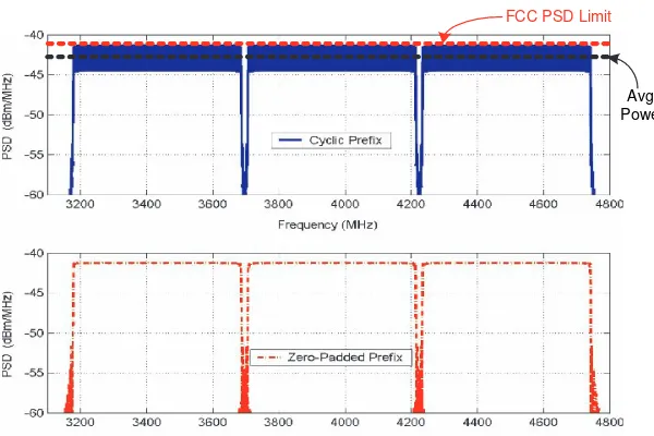
The field of wireless communications has recently witnessed the emergence of technologies characterized by channel bandwidths that are of the same order as the carrier frequencies. For example, the ultra wideband (UWB) system employs a frequency spectrum spanning 3.1–10.6 GHz, with a minimum channel bandwidth of 500 MHz. UWB is a low-power system that utilizes a power level for transmis-sion that is below the FCC limit on spurious emistransmis-sions (<–41.3 dBm/MHz) [1]. The small power density is necessary to ensure that UWB can coexist with other systems, without causing performance degradation. As a consequence the system is also relatively short distance, especially when used for high-data rate applications. It is intended for a diverse set of applications such as high-speed communications, biomedical applications and short-distance radar.
UWB represents a fundamentally different way of designing wireless systems in comparison to most current wireless communication systems that are predom-inantly narrowband, that is the carrier frequency employed is significantly larger than the channel bandwidth, such as, e.g., in cellular telephony. Current narrowband systems rely primarily on increasing channel SNR to enhance capacity, since they
R. Gharpurey
Department of Electrical and Computer Engineering, University of Texas, Austin, TX 78712, USA e-mail: [email protected]
R. Gharpurey, P. Kinget (eds.),Ultra Wideband, 1
C
2 R. Gharpurey, P. Kinget
operate in a highly spectrum-constrained environment, while UWB systems rely primarily on bandwidth. Broadband wireless redefines circuit design techniques and requirements, transceiver and synthesizer architectures and system considerations compared to narrowband systems. Additionally, given that narrowband front-end filters cannot be employed, in-band interference and coexistence with other systems become a major consideration.
This text is meant to provide the reader with an overview of the state of the art in various aspects of ultra wideband technology. The book includes description of cir-cuit techniques, architectures and system considerations, while addressing emerging challenges in the field. System-level issues are discussed in Chapters 2 and 3, while Chapters 4–6 present implementations of various types of UWB transceivers for pulse-based and OFDM-based systems.
Chapter 2 by Foerster et al. describes system implementations that have been proposed for UWB communications. It covers issues fundamental to UWB system design, such as multipath performance, channel response, processing gain, multiuser access, implementation and link budgets, initial acquisition and narrowband inter-ference. An overview of pulse-based and OFDM-based techniques for UWB com-munication systems is presented. System-level enhancements such as detect and avoid for interference mitigation are also described. The chapter relates UWB to another emerging development in the field of broadband wireless, namely cognitive radios.
Chapter 3 by Stephan ten Brink et al. discusses baseband architectures for ultra wideband communication systems based on the multiband OFDM approach. As-pects from preamble processing such as packet detection, frame synchronization and frequency offset estimation illustrate the challenges posed to reliable detection and synchronization over wideband channels. Algorithms, performance benefits and implementation costs of several next-generation high rate extensions are described in detail, including higher-order modulation as well as different multiple antenna techniques.
Chapter 4 by Razavi et al. presents an implementation of a direct-conversion UWB transceiver for MB-OFDM using the 3–5 GHz band. Three resonant networks are used at the input along with three phase-locked loops for carrier generation. Typ-ical specifications for the analog section of an MB-OFDM transceiver are presented in this chapter.
Chapter 5 by Lee et al. describes a pulse-based UWB transceiver. The signaling is based on a 500 MHz sub-band approach utilizing the full bandwidth from 3.1 to 10.6 GHz. The chapter includes a description of the RF front-end and transmitter sections, as well as the baseband used in the design. A description of the antennas used in the test setup is also provided. Synchronization requirements and the design of a RAKE receiver for addressing multipath are presented.
authors. Architectural issues in such systems such as timing and synchronization are addressed in detail.
The discussion in this chapter focuses on some of the critical bottlenecks in circuits for ultra wideband systems, with an emphasis on the problem of achiev-ing broadband gain. Most of the challenges in UWB circuit design in fact arise from the broadband nature of the designs, which necessitates much greater gain-bandwidth products than have been required of narrowband radio front-ends. As we will discuss briefly, this aspect of the system also leads to a key bottleneck arising from the potential for interference-related degradation of the system. Other chal-lenges include the requirement for fast-hopping signal sources in multiband schemes capable of spanning the entire UWB band. Several other design issues relevant to the analog section of these transceivers are also addressed. Some of these issues are relevant to all UWB implementations, while other challenges are more system specific.
1.2 Front-End Designs for UWB Systems
The front-end of UWB transceivers is similar across different standards, such as pulse-based (e.g. [2]) and multiband approaches, and depends primarily on the full band covered by the system. In the case of pulse-based systems, the signal may be down-converted to baseband through a mixer or else a correlator-based approach may be used for detection as discussed in Chapters 5 and 6. In the multiband OFDM approach [3] a mixer is used to down-convert the incoming spectrum to the desired IF frequency or baseband in the case of direct-conversion implementations, and the signal is then filtered and quantized. The receiver chain in this case looks very sim-ilar to that employed in a narrowband system.
Regardless of the down-conversion approach used, the front-end amplifier has to have the ability to process the entire desired bandwidth. The design specifications are similar to narrowband amplifiers and include gain, noise figure, input matching, measures for linearity such as the 1 dB input compression point and intermodulation intercept points. The key difference is that these metrics have to be achieved over a broad signal bandwidth, which is of the same order as the center frequency of operation.
4 R. Gharpurey, P. Kinget
on the transmitted power density of –41.3 dBm/MHz. This limits the output power requirement of the transmit amplifier to be of the order of approximately 0–3 dBm. The amplifier topologies discussed below are all capable of providing this level of output power. Thus much of the discussion below is relevant to the output stage at the transmitter as well.
1.2.1 Resistive Matching and Noise Cancellation Techniques
The use of resistively loaded amplifiers is motivated primarily by the requirement for area efficiency in short-channel CMOS technologies. While other techniques discussed later can offer much higher power efficiency and dynamic-range perfor-mance, the use of integrated inductors for tuning and matching may lead to unac-ceptably high area requirements.
The input amplifier in addition to providing gain also needs to be matched to the external source impedance. Two approaches that can be employed for this pur-pose include common-gate designs that have input impedance proportional to the inverse of the device transconductance and resistive-feedback-based designs, such as a shunt–shunt feedback topology. Negative feedback is a classical technique for increasing amplifier bandwidth [4, 5]. Since the UWB band extends up to 10.6 GHz, in order to achieve adequate gain in a single stage the gain-bandwidth product of the devices needs to be of the order of 100 GHz. It is only recently that CMOS devices with such performance have become available in the commercial space. Al-ternatively cascaded sections can be used to enhance the equivalent gain-bandwidth product beyond that of a single stage. However, this can lead to degradation in lin-earity and a loss of power efficiency.
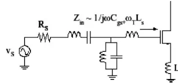
A simple shunt–shunt resistive-feedback circuit is shown in Fig. 1.1a. This design has an input impedance of (RF + RL)/(1 + gmRL), a voltage gain of
–gm(RL||RF)/2, assuming input matching, and can be designed to provide the
desired output impedance level, by appropriate choice of the feedback resistance RF. Ccis a large ac-coupling capacitor.
One of the key issues in this design, and similarly in a common-gate design (Fig. 1.1b), is that the input impedance looking into the amplifier is restricted to the impedance of the source Rs, typically 50 Ohms. This severely restricts the
flexibil-ity in choosing the value of the transconductance of the input device. In the limit that RL tends to infinity, the input impedance of a shunt–shunt amplifier equals the
inverse of the device transconductance which is thus constrained to be equal to the conductance of the source. Similarly the transconductance of the input device of a common-gate design also has to equal the conductance of the source.
A consequence of the fixed value of the input transconductance is that the noise figure of the amplifier is also determined by the input power matching requirement. The voltage gain for the case when RLtends to infinity is given by
AV =
1−gmRF
2 (1.1)
It can be shown through noise analysis that the noise factor for the amplifier at low frequencies is given by
F =1+ RF Rs
4 (1−gmRF)2
+γ(1+gmRF)
2
(1−gmRF)2
(1.2)
Thus as the gain is increased by increasing the value of RF, the noise factor
asymptotically approaches 1+γ, whereγis 2/3 for long-channel devices and higher for short-channel length devices. It should be noted that this is a best-case result and in practice the noise factor will be higher, especially as frequency increases, and becomes a significant fraction of the device cut-off frequency.
The noise factor of a common-gate device at low frequencies, with its input impedance matched to the source, is given by
F =1+γ +4RS RL
(1.3)
and the gain by gmRL/2. Thus as the gain is increased by increasing the value of RL,
the noise factor similarly asymptotically assumes a value of 1+γ. This result also assumes that the common-gate amplifier utilizes an RF choke to connect the source to the ground. If a resistor or current source is used instead for biasing the device, the noise factor will increase above this ideal value.
6 R. Gharpurey, P. Kinget
impact on the input impedance in the case of shunt–shunt amplifier, while this is not so in the common-gate case.
The basic shunt–shunt feedback and common-gate amplifier topologies cannot typically be used directly in UWB front-ends, primarily due to inadequate noise performance over the desired bandwidth, as well as potentially inadequate gain-bandwidth product of the input device. The gain-bandwidth of the amplifiers may be severely limited at high gain due to capacitive loading at the output and the resulting pole. The single-transistor topologies thus need to be enhanced to achieve the desired noise, gain, bandwidth and linearity specifications.
The gain-bandwidth product of amplifiers can be significantly increased by using inductively tuned loads, through the use of appropriate design techniques. For example, one design approach applicable in the broadband case is the use of multiple stagger-tuned stages. While well suited for enhancing electrical performance, the added area penalty may not be acceptable in short-channel processes.
A compromise between the conflicting requirements of bandwidth and area is of-fered by applying the shunt-peaking technique, by adding an inductor in series with the load resistor [5]. At higher frequencies, as the impedance of the load capacitance decreases, that of the series combination of resistance and inductance increases. By properly controlling the relative values of the load resistance and inductance in rela-tion to the parasitic capacitance, a flat gain can be achieved over wider bandwidth. In fact, a bandwidth extension of as much as 70% can be achieved by use of a single inductor, in comparison to a simple shunt R–C load. The inductor does not require a high-quality factor, since it is in series with a relatively large resistor. Thus, in integrated applications, the interconnect trace used to implement the inductor can be kept relatively thin, thereby further minimizing area penalty [6]. Shunt-peaking can be used in both shunt–shunt and common-gate designs to increase the bandwidth, without leading to excessive area penalty, thus retaining the motivation behind the single-stage design.
Another effective technique for increasing the gain-bandwidth product of a single-stage amplifier is to cascade multiple stages [5]. If an amplifier has a constant gain-bandwidth product, then by using many of these stages in cascade, where each stage provides a low level of gain, an overall gain-bandwidth that is much greater than that of the single-stage amplifier can be achieved.
The design in [6] combined the cascade approach with shunt-peaking to imple-ment a front-end LNA with a flat-gain bandwidth from 2 to 5.2 GHz, gain of 16 dB, a noise figure of 4.7–5.7 dB in the UWB band. The power dissipation in the design was 38 mW and the design was implemented in a 0.13µm CMOS technology and measured in a low-cost BGA package. The design also provided single-ended to differential conversion. A combination of cascading and shunt-peaking was also reported in [7]. The design was employed as the front-end LNA of a 3.1–9.5 GHz UWB transceiver and provided a cascaded gain of 27 dB. It was implemented in a 90 nm CMOS process. A 5GHz CMOS LNA that employed a gm-boosted
The topology was inductor-less resulting in a very low area requirement and utilized dual-feedback loops. The power required for this amplifier was 42 mW.
Besides limited gain-bandwidth product, the other major design limitation of single-stage amplifiers of Fig. 1.1 is that the best-case noise figure is directly de-termined by the input matching requirement. We observe that the noise figure is ultimately limited by the noise generated by the input device for large values of gain. A solution for decoupling the noise and matching performance was presented in [9]. The key elements of the idea are shown in Fig. 1.2. This design utilizes a unique property of the shunt–shunt amplifier: while the amplifier provides a phase inversion for the signal path, the drain noise of the input device appears in phase at the gate node. Thus if the signal at the gate node is inverted and combined with the signal at the drain node, it is theoretically possible to cancel the drain noise arising from the input device by using the appropriate ratio in the combiner. The noise at the output is dominated by the noise of the signal combiner, which can be minimized by increasing the gain of the combiner at the cost of higher power dissipation. The input matching is still set by the transconductance of the input device, but this de-vice does not contribute to the output noise. The implementation shown in Fig. 1.2 shows a combiner that uses the upper and bias devices of a source follower stage for generating signals with opposite polarity. This technique results in a noise factor given by [9]
F =1+ RS RF
+ γ
gm,2
1 RS
+ 3
RF
+2RS
R2F
(1.4)
For large values of gm,2, and for RF >> RS, this expression asymptotically approaches
F ≈1+ RS RF
(1.5)
In effect, this technique allows the designer the flexibility to trade off power dis-sipation with noise performance, while not affecting the input match. An amplifier
8 R. Gharpurey, P. Kinget
using a common-gate input can also be similarly modified to decouple the noise performance and the input matching requirement, if the source point of a common-gate device is applied to a second common-source amplifier. Such a technique was presented in [10]. The key elements of this approach are shown in Fig. 1.3a, where we assume that the source resistance is matched to the input transconductance of the common-gate device. For this condition, it can be shown that the noise contribution of the common-gate device can be nulled at the differential output observed across the drains of the common-gate and the common-source devices, M1and M2,
respec-tively, if the voltage gain of the common-gate stage from its source to its output is made equal to that of the common-source stage from its gate to its output [9]. In packaged amplifiers, the transconductance of the common-source device becomes frequency dependent due to the parasitic source impedance presented by the bond-wires of the package, which may lead to non-ideal cancellation.
The dominant noise source at the differential output is that of the common-source device. If the transconductance of the common-source device is made equal to that of the common-gate device, then the noise figure is effectively equal to that of the common-gate stage which is not a useful result. On the other hand, the require-ment for noise cancellation is merely that the voltage gains of the common-gate and common-source stages be made equal, which can also be achieved by using a larger transconductance of the common-source device, with a smaller load impedance, such that the product of the two equals that within the common-gate stage. The output noise contribution of the common-source stage is given by 4 kTγgm,2RL22or
equivalently 4 kTγ (gm,2RL2)2/gm,2. Under the constraint that gm,2RL2 is constant,
increasing gm,2 can be seen to decrease the output noise voltage of the
common-source device. As before, this implies a trade-off between noise performance and power dissipation.
An added benefit observed in this implementation is that it is an inherent single-ended to differential converter and obviates the need for an external broadband
balun. The front-end amplifier in [10] combines the above approach with shunt-peaking, to achieve broadband gain of 19 dB over a bandwidth of 0.1–6.5 GHz, with a noise figure of 3 dB and a power dissipation of 12 mW in a 0.13µm CMOS process.
The design in [11] also employs noise cancellation utilizing a common-gate input device. However, the output is combined in a single-ended manner, after a second inverting amplifier is used at the load of the common-gate device. A conceptual view of this design is shown in Fig. 1.3b, where Ccis a large coupling capacitor.
The amplifier also employed shunt-peaking and achieved broadband performance from 1.2 to 11.9 GHz with an in-band gain of 9.7 dB, a noise figure in the range of 4.5–5.1 dB, an IIP3 of –6.2 dBm and was implemented in a 0.18µm CMOS process. A key consideration in the design of UWB front-ends is interference robustness. This is a very important issue, since given the broadband nature of UWB, the system is inherently susceptible to jammers that can arise from a multiplicity of sources, including intentional transmitters such as cellular phones and WLAN systems. A particularly challenging interferer is the UNII-band WLAN system at 5 GHz that appears in the center of the UWB bandwidth. This issue is introduced in Section 1.5 and a detailed treatment is provided in Chapter 2.
1.2.2 Broadband Input and Output-Matched Amplifiers
Another approach to broadband designs for UWB front-end amplifiers is to use high-order reactive matching networks [12, 13]. This type of design has also been employed by Zheng et al. in Chapter 6. The design of passive networks for broad-band matching is a subject of classical network theory [14, 15]. It can be treated as an impedance matching or a filter-synthesis problem. In contrast to the techniques discussed in the previous section, the above techniques provide ideally lossless matching by the use of passive reactive elements. Such techniques are thus capable of providing significantly better gain and dynamic-range performance normalized to power dissipation than those discussed previously at similar channel lengths, but at the expense of requiring multiple integrated inductors, with the associated area penalty.
10 R. Gharpurey, P. Kinget
Fig. 1.4 A 3rd-order bandpass network for input impedance matching
A 3rd-order bandpass network for broadband input matching of the gate of a common-source device is shown in Fig. 1.4 [12]. The band-pass nature of the net-work can be deduced by observing that the netnet-work acts as an attenuator near DC as well as in the high-frequency limit. The matching network transforms the impedance seen looking into the input of the device to the source resistance. Thus the real part of the input impedance is transformed to this value of resistance, and the reactive part is ideally canceled over a broad spectrum. Parasitic inductance of packages can be easily absorbed in such designs. The technique of synthesizing a lossless real part in the input impedance by utilizing the bond-wire inductance of the package can be employed in these matching networks as well, since to the first order the real part to the input impedance is given bytLs, where Lsis the degeneration inductance. This
is independent of frequency, and thus can be used as the load resistance of the input matching network [12, 13].
The design of [13] employed a SiGe BiCMOS technology and provided a power gain of 21 dB, with a noise figure in the range of 2.5–4.2 dB from 3 to 10 GHz, and an IIP3 of –1 dBm with a power dissipation of 30 mW. The design presented in [12] was implemented in a 0.18µm CMOS process, and reported a gain of 9.3 dB, a noise figure of approximately 4–8 dB across the frequency band from 3 to 10 GHz and an IIP3 of –6.7 dBm with a power dissipation of 9 mW.
Simultaneous noise and power matching can be challenging in such networks. It can be shown through analysis that the optimal noise reactance at the input of an inductively degenerated device is approximately –1/jCin. Thus a broadband
matching network that provides a conjugate match to the source impedance will provide the optimal noise reactance to the first order. The real part of the optimal noise impedance, however, is also frequency dependent. Thus the matching network, which provides a constant real part looking into the source, may not match the noise resistance over all desired frequency bands.
These networks provide voltage gain from the source to the gate of the MOSFET, which is a consequence of the typically higher impedance of the MOS input com-pared to the source resistance. In fact a substantial portion of the gain may be achieved through the passive matching network. This can degrade the compression point of the active device, as in the narrowband case.
combination of the input capacitance and a series resistance of valuetLs. For this
impedance, if⌫() is the frequency-dependent reflection coefficient looking into the series R–C load, then the Bode–Fano criterion places the following bound on the input match:
In the above expression,0is the center frequency of operation. In an ideal
band-pass match,⌫() is set to 1 outside the bandwidth of interest and is less than 1 within the band of interest, implying power delivery to the load. If the desired band is B and we design for a constant in-band reflection constant⌫0, then the above
expression places a lower bound on the value of⌫0to be
Γ0≥e
For a constant RC product and center frequency, the Bode–Fano criterion places a limit on the best possible constant match that can be achieved in practice, assuming an ideal passive matching network. Alternatively, instead of achieving a constant match over all frequencies, it is possible to achieve a very good match over narrow frequency bands, at the expense of a worse match at other frequencies within the band of interest [15].
A key challenge in the use of such designs, especially in comparison to the broad-band resistively matched techniques of the prior section, is their area requirement which is typically in the range of a square millimeter or more. This area requirement can be expensive in short-channel CMOS processes. Many designs have reported measurements in an on-wafer probe environment, rather than in a package, which can have significant impact on the performance. On the other hand, the input and ground path package inductance can be absorbed into the matching network with relative ease using these techniques.
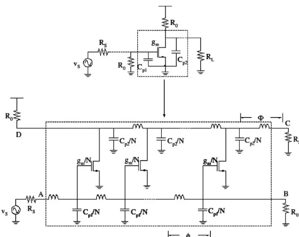
1.2.3 Distributed Amplification
Distributed amplifiers also provide broadband input matching; however, the ap-proach taken is different compared to the broadband matching technique consid-ered earlier. In this type of amplifier (Fig. 1.5), a single large device is divided into multiple smaller sections, each with smaller unit input and output capacitance. The capacitance of the unit devices is absorbed into a lumped approximation of a broadband transmission line, at both the input and the output, by using discrete inductors. The input transmission line is terminated in a matched resistive load R0,
12 R. Gharpurey, P. Kinget
Fig. 1.5 A resistively matched common-source amplifier and its distributed amplifier equivalent
this way, the input source and the output load see a broadband matched termination looking into the input and the output of the amplifier, respectively. Following the discussion from [16], we assume that the signal is shifted in phase byat the input and⌽on the output lines by each subsequent device. For identical phase delays on the input and output transmission lines, the broadband power gain from the input node A to the output node C can be shown to be
GF = n2g2
mRLRS
4 (1.8)
wheren is the total number of stages in the amplifier, gm is the transconductance
of each stage, RLis the load resistance and RSis the source resistance. The voltage
gain of the amplifier is limited by the impedance of the loads employed at the input and output terminations.
such cases, the output resistance may need to be kept relatively small, to extend the bandwidth. Thus the voltage gain of these amplifiers is typically limited. Enhance-ment of voltage gain can be achieved through the use of matrix amplifiers, which are the distributed analogues of cascaded single-stage amplifiers, but these are likely to be too power-hungry for UWB applications, in addition to requiring excessively large die area.
The power delivered to the output transmission line can flow towards both the output load and the termination at node D. The gain from the input to the drain termination is referred to as the reverse gain of the amplifier and is given by [16]
GR =
gm2RLRS 4
si n(n(ϕ+Φ)/2) si n(ϕ+Φ)/2
2
(1.9)
The above gain is significantly reduced within the band of interest due to cancel-lation of the drain current towards the termination, as a consequence of destructive interference. Proper phase combining ensures that the desired signal is forced to propagate towards the output, where the drain currents add constructively.
The reduction of reverse gain within the band of interest has very interesting implications for noise. Since the noise of the input line termination resistor is scaled by the reverse gain when it reaches the output load at C, we see that this noise is reduced significantly. Thus the input line termination resistor provides an input power match, but does not provide substantial noise at the output. This is a key advantage provided by the distributed topology, similar to the decoupling of noise and impedance matching in the noise-cancellation stages discussed earlier.
The noise figure of the distributed amplifier can approach that of a narrowband noise-matched common-source amplifier, although over a much broader bandwidth. This behavior is seen in recent examples of distributed amplifiers that show a smaller variation in noise figure across the frequency bandwidth compared to those employ-ing multi-section broadband matchemploy-ing.
The gain-bandwidth product of distributed amplifiers is limited primarily by the input and output transmission lines. Since these lines are discrete, their characteristic impedance changes with frequency. As shown in [17] this cut-off frequency is given by 1/πRCg, where R is the input resistance and Cg is the gate capacitance of an
individual device. For ann-stage distributed amplifier, the gain-bandwidth product to the first order is then given byngm/2πCg, where gmis the transconductance of a
single device.
The above expression succinctly captures the advantage provided by distributed amplification. A single device with transconductance gm and capacitance Cg has
a gain-bandwidth product of gm/2πCg(∼ft). In a distributed amplifier, the
gain-bandwidth product scales linearly with the number of unit devices (n).
14 R. Gharpurey, P. Kinget
increasing attenuation before it reaches the output load. Consequently there exists an optimal number of stages at which the gain-bandwidth is maximized.
Ignoring the losses in the input and output lines and using the ideal expression for the gain-bandwidth product, we can derive interesting insights into the optimal biasing point of the device used in a distributed amplifier, utilizing a figure of merit given by the ratio of the gain-bandwidth product to the total bias current used in the amplifier. For a MOS device, the gm/I ratio is high in weak- to moderate inversion,
that is for sub-threshold operation. However, the cut-off frequency is also lower than the strong-inversion case. By usingndevices in weak inversion, the effective gain-bandwidth can be enhanced over that of a single device, while retaining the higher overall gm/I ratio of the amplifier. The above reasoning was described in [19] and
used to implement a CMOS distributed amplifier with moderate inversion device operation. The amplifier was implemented in a 0.18µm CMOS process, demon-strated a gain of 8 dB from 0.04 to 6.2 GHz, with a noise figure of 4.2–6.2 dB and an IIP3 of 3 dBm at a power level of 9 mW.
An interesting feature of distributed amplifiers is that since there are no high-impedance nodes within the amplifier, the voltage levels at the input and the output are relatively small, for example in comparison to approaches such as those us-ing multi-section LC matchus-ing. Consequently, distributed amplifiers also happen to exhibit high output 1 dB compression point, compared to any of the topologies discussed to this point. Thus these amplifiers are also very well suited for the out-put buffers used in UWB transmitters. The transmitter outout-put stages in UWB need relatively modest output 1 dB compression points of the order of 2–3 dBm. This has been demonstrated in DAs even for low-voltage CMOS technologies, e.g., [19] and [20], which reported a DA with 10.6 dB gain from 0.5 to 14 GHz bandwidth, a noise figure of 3.4–5.4 dB and an output 1 dB gain-compression point of 10 dBm at a power dissipation of 52 mW, in a 0.18µm CMOS technology.
the impact of the ground inductance is to use a differential amplifier topology, although this requires the use of a broadband balun externally, the design of which is non-trivial.
The bond-wire inductance on the input can be absorbed into the input line if the interstage inductance in the amplifier is larger than the bond-wire inductance; however, this may not always be the case, especially in high-frequency designs. The bond-wire inductance can be decreased by using multiple bond-wires in parallel but this has the undesirable side effect of simultaneously increasing the bond-pad capacitance that loads the input node.
It is perhaps due to the above practical considerations that most reported UWB transceivers have in fact not utilized DA topologies. On the other hand, the topology continues to be of significant interest, and if a low-cost solution is found to the packaging parasitics, will doubtless be well utilized, owing to its excellent dynamic-range performance per unit current.
1.3 UWB IF: Mixers, Variable Gain Amplifiers, Filters
and A–D Converters
This section outlines the circuits that comprise the IF section of a UWB transceiver. Much of this portion of the transceiver is system specific, unlike the earlier designs for front-end amplification techniques that were fairly independent of the system it-self. As such the discussion is brief, and for detailed insights references are provided to the appropriate chapters in the text. It should be mentioned that the broadband design issues discussed earlier are significant in some instances in the IF section as well, for example for broadband variable gain amplification, and at the input stage of mixers. In other cases, the designs can borrow directly from techniques employed in traditional narrowband receivers while redesigning for higher bandwidths although with relatively limited dynamic range. Since the baseband in the system extends to 250 MHz in the multiband OFDM approach and over 2 GHz in many of the pulse-based schemes, significant modification is required, as they are especially sensitive to parasitics.
1.3.1 Mixer Design for UWB
16 R. Gharpurey, P. Kinget
to drive a passive switch-based down-converter or a current-commutating switching stage. A switch-based down-converter requires large swing and does not have inter-nal nodes with low impedance. It is thus preferable to use a current-commutator design instead. Given the broad bandwidth of the channels, even in the case of multiband systems, a usually important disadvantage of MOS current-commutating mixers, namely in-band flicker noise, is not a significant consideration in this case.
The mixers used in pulse-based UWB systems are usually employed as corre-lators, where they can be used as part of the receiver-matched filter. The circuit operation is similar to the above case and therefore not repeated here. The reader is referred to Chapters 5 and 6 for implementations of such designs.
1.3.2 Variable Gain Amplifiers
In a typical pulse-based approach to UWB, the UWB band is down-converted to baseband for an aggregate baseband channel of approximately 1 GHz, for the lower band of 3–5 GHz, and 2 GHz for the upper band of 6–10 GHz. Several pulse-based approaches limit the input signal and therefore do not require significant levels of gain control. In the MB-OFDM approach to UWB, the channel bandwidth is rel-atively much narrower, of the order of 250 MHz. The gain variation requirement can be of the order of 40–50 dB, with a peak-gain requirement of the same order, depending on the specific architecture. A peak gain of 50 dB with a bandwidth of 250 MHz corresponds to a gain-bandwidth of 75 GHz, which is similar to that required in the front-end LNA. Thus VGA designs for MB-OFDM UWB can be challenging.
It is typically not possible to achieve the high peak-gain requirement in one stage of amplification, while simultaneously achieving the desired bandwidth. An effec-tive technique for broadband variable gain implementation is to use cascaded stages of amplifiers [5] to achieve the desired bandwidth. This also improves the attenua-tion of out-of-band interferers, since cascaded stages have a sharper high-frequency roll-off for the same effective gain-bandwidth product, compared to a single-stage amplifier.
VGA functionality has been demonstrated in recently reported UWB transceivers using multiple techniques. Some degree of gain switching is usually required in the front-end LNA (see Chapter 4), especially to accommodate large interferers. If broadband VGA functionality is required over the full UWB band, or a significant fraction of it, then distributed amplification offers an excellent approach to cas-caded stages. As discussed earlier, these stages can maintain low input- and output impedance and can be used to provide broadband matching. The design from [19] was demonstrated to have variable gain from –10 dB to 8 dB, for a bandwidth from DC to 6.2 GHz, where the gain flatness and matching performance were maintained over the gain tuning range.
be distributed between filter stages, to maximize the overall dynamic range of the baseband stage. In [21], the authors employ a passive switched attenuator between filter stages. In [22], the VGA is implemented as a switched transconductor and a variable gain buffer, the first circuit before the filter, and the second after the filter. A VGA based on a Gilbert-cell multiplier is employed in [23]. As discussed in Chapter 4 a key challenge in the MB-OFDM system is handling DC offsets within the VGA chain, since the DC offset in response to a gain step needs to settle very rapidly, in fact within nanoseconds.
1.3.3 Filter Design for UWB
Pulse-based UWB systems employ correlators and matched filters for spectral shap-ing, band limiting and detecting signal energy. Such implementations are presented in detail in Chapters 5 and 6.
Multiband OFDM implementations require strict bandwidth controls. Typically 4–5th order filter topologies have been employed for channel selection and filtering of adjacent channel interference in these implementations. For example in [22], the authors present a 5th-order Gm-C filter with a corner frequency of 240 MHz in a 0.13-µm CMOS technology with a power dissipation of 24 mW and input referred noise of 7.7 nV/sqrt(Hz). The gain of the filter is 48 dB which includes the gain of the VGA, embedded within the design. A 5th-order Tchebycheff design is employed in [21] with a gain range from 16 to 46 dB and a tunable bandwidth from 232 to 254 MHz. A 4th-order Tchebycheff design is described in [24] with a nominal corner frequency of 259 MHz. Two cascaded 3rd-order elliptic filters are employed in [7]. A passive LC 5th-order elliptic low-pass channel select filter is employed in [23].
1.3.4 Data Conversion for UWB
In OFDM-based approaches, the baseband ADC in the receiver can be a challenging design, more so than the DAC in the transmitter. Given that for the MB-OFDM approach, the baseband bandwidth is of the order of 264 MHz, the sampling rate required in the ADC needs to be at least 528 MHz. On the other hand, the resolution requirement is limited [3], of the order of 4–5 bits.
18 R. Gharpurey, P. Kinget
Substantially lower power requirement has been reported by the use of successive approximation (SAR) approaches. A 5-bit time-interleaved SAR requiring a power consumption of 6 mW was demonstrated in [28] using a 65 nm CMOS technology. Another 5-bit SAR was also demonstrated in a 0.18µm CMOS technology, with power requirement of 7.5 mW [29].
DAC designs for MB-OFDM UWB are relatively easier, owing to the limited resolution. Current-steering DACs can easily be employed for this purpose and are not detailed here. DAC designs for the transmitter sections of pulse-based UWB sys-tems on the other hand pose much more design challenge, owing to their broadband nature. Additionally these are usually tailored to specific system implementations and often are integral to the final spectrum shaping functionality. Examples and design details can be found in Chapters 5 and 6.
1.4 Frequency Synthesis in UWB
Pulse-based schemes in UWB can employ correlators for detecting the energy in the transmitted signals and, thus in some implementations, may not require an explicit frequency synthesizer. For utilization of the upper band (6–10 GHz), it may be nec-essary to down-convert the band to baseband and thus a fixed carrier at mid-band can be employed [30].
Multiband solutions including MB-OFDM employ relatively narrower channels and cycle through these bands in order to utilize the entire UWB spectrum. The time required to hop and settle the frequency between successive steps needs to be minimized and is of the order of 2 ns in the MB-OFDM system [3]. Phase-locked loop-based synthesizers, such as those utilizing the integer-N architecture, would be challenging for this purpose due to settling time limitations, as well as other issues such as an excessively high oscillator center frequency, of the order of the lowest common multiple of all center frequencies, and the need for extremely fast dividers running at several decades of GHz. A solution proposed for this problem employed an oscillator with a fixed center frequency, where the output frequency was divided and combined through single-sideband mixing to generate the desired channel frequency [3, 31]. The original proposal assumed a center frequency of 4224 MHz, which was divided by 4 to provide 1056 MHz and further divided by 4 to provide 264 MHz. By using single-sideband mixing, these bands could be com-bined to provide center frequencies at 3432, 3960 and 4488 MHz. Band-selection in single-sideband mixing is accomplished by merely changing the polarity of the single-sideband combiner. Since this is an open-loop operation, it is inherently fast, as no feedback-related settling dynamics are involved and the only limitations on speed arise from the load parasitics at the output of the combiner.
demon-Fig. 1.6 Open-loop synthesis of output frequencies through frequency division and image-reject mixing
strated in a 0.18µm CMOS process that employed two PLLs with outputs at 6336 and 3960 MHz and their divided outputs; a two PLL solution for the lower band [21] that was demonstrated in a RF-BiCMOS process; and a 7-band solution [33] span-ning 3–8 GHz that was implemented in a 0.18µm CMOS process. All the above solutions demonstrate band switching speeds of the order of nanoseconds. An ap-proach by [34] utilized direct digital synthesis (DDS) for implementation of one of the bands for a 3–5 GHz UWB implementation. DDS technologies promise to be an exciting alternative to mixer-based approaches, especially with short-channel technologies below 90 nm, as they can be used to provide outputs with low spurious levels.
1.5 Interference and UWB
Isolation between users of different systems in narrowband wireless systems is achieved largely by spectral separation. Cellular standards such as 3G-WCDMA, for example, employ an exclusive band for operation. Broadband wireless schemes such as UWB on the other hand receive and transmit signals over vast portions of the spectrum. Thus coexistence and interference of broadband wireless systems with other systems become critically important. The wide bandwidth also substantially increases the scope for interference in the front-end due to substrate- and package-coupling. The potential for in-band interference can have a significant impact on the design of the RF and analog section of the transceiver. Without the use of specialized techniques, the front-end is exposed to all large jammers that can exist in the system, and this can place correspondingly large linearity requirement in the front-end. A brief overview of interference and coexistence issues is presented below. The reader is referred to Chapter 2 for detailed analyses and insights into this issue.
1.5.1 External Interference and Coexistence
20 R. Gharpurey, P. Kinget
on WCDMA [31]. With an omni-directional antenna, a combination of transmit filtering and frequency separation is required in order to ensure coexistence. Similar considerations apply for co-existence with systems such as IEEE 802.11b, 802.11a and 802.15.4.
UWB receivers themselves can be the victims of large in-band radiators from other systems. UNII-band transmitters in the 5.1–5.85 GHz band are major sources of interference for UWB. Many UWB frequency plans, including the multiband OFDM approach and certain pulse-based implementations have an option to exclude the UNII-band altogether. It is interesting to note that if two UNII-band systems are used simultaneously for transmission (e.g., at 5.3 and 5.8 GHz) in-band 3rd-order intermodulation can be a design issue even in UWB systems that avoid the UNII bands. Interferers that can lead to in-band IM3 products and the UWB bands that they impact are identified in [35].
Spurious radiation introduced by other commercial systems can also limit the performance of UWB. For example, the specifications for WCDMA mobile trans-mitters allow for a spur level as high as –30 dBm in a 1 MHz bandwidth from 1 to 12.75 GHz, which can be within the channel bandwidth of a UWB system [31]. An emerging system that can have significant coexistence and interference issues with UWB is WiMAX. A detailed analysis of these issues, with simulation results indicating the potential degradation in UWB, is described in Chapter 2.
To minimize degradation caused by such an in-band spur, the analog dynamic range will need to be sufficiently large. One technique to alleviate this requirement is to increase the resolution in the baseband ADCs. This can be power hungry, since the converters typically run at high sampling rate (>500 Ms/s). Further the bit-width of at least a part of the baseband digital path would need to be increased, which will also increase overall system power requirement. If the dynamic range of the receiver is insufficient, for example if the analog section saturates in the presence of an in-band spur, it will result in the loss of useful information in part of the bandwidth in a sub-band approach. If the modulation uses the entire band, a large in-band spur can pose a significant challenge. Saturation of the signal chain in this case will impact the entire band.
In theory, therefore, the dynamic range can be split between the auxiliary receiver, which detects the large signals, and the main path receiver, which can avoid the large signals, and thus has a reduced linearity requirement. The dynamic range is thus relaxed in both the main and auxiliary receiver paths.
1.5.2 Interference Due to Circuit Activity
Low-cost, highly integrated solutions are critical to the adoption of broadband wire-less as a viable technology for commercial high-speed communication applications. It can be expected that UWB solutions featuring increasingly higher levels of in-tegration will appear in the near future. Amongst the most significant unknowns at this time in the development of highly integrated UWB systems is the potential cou-pling of interfering signals generated by on-chip circuit activity, through substrate and package parasitics. The scope for such coupling is significant due to the wide bandwidth and can prove to be a bottleneck for highly integrated implementations. UWB systems can require large digital circuits of the order of hundred thousand gates or more, such as FFT cores that operate at several hundreds of MHz. It is possible that in a highly integrated UWB system, the sensitivity of the system is limited not by the thermal noise at the input, but by the above signal coupling. Spectral domain isolation, e.g., spur planning, is very often exploited in narrowband systems to maximize integration level, but will be difficult to employ in UWB. The ability to estimate the level of self-induced noise in potential implementations will be a key requirement for future broadband standards and integrated architectural solutions. A discussion of this can be found in [38].
1.6 Summary
Ultra wideband represents a fundamentally different way of implementing wireless communication systems. The two key attributes that distinguish this system include the broadband nature of the system, where the channel bandwidth is a significant fraction of the carrier frequency; and the approach used for coexistence with other systems, which relies on low power-spectral density for transmission and reception, rather than strict isolation in the frequency band. These characteristics have neces-sitated the development of new techniques at the circuit, architecture and system levels. Thus it promises to be an exciting space for innovation in wireless technolo-gies. The following chapters in the text are representative of various aspects of this innovation.
22 R. Gharpurey, P. Kinget
References
1. FCC 02-48A1, First R&O: revision of part 15 of the commission’s rules regarding ultra-wideband transmission systems, (available online at http://hraunfoss.fcc.gov/edocs_public/ attachmatch/FCC-02-48A1.pdf)
2. XtremeSpectrum CFP document, R. Roberts, IEEE P802.15-03/154r3, (available online at http://grouper.ieee.org/groups/802/15)
3. Multi-band OFDM physical layer proposal, A. Batra et al., IEEE 802.15-03/267r1, (available online at http://grouper.ieee.org/groups/802/15)
4. Analysis and design of analog integrated circuits (4th Edition), P. R. Gray, P. J. Hurst, S. H. Lewis and R. G. Meyer, Wiley, 2001
5. The design of CMOS radio-frequency integrated circuits, (2nd Edition), T. A. Lee, Cambridge University Press, 2004
6. A broadband low-noise front-end amplifier for ultra wideband in 0.13-µm CMOS, R. Gharpurey, IEEE Journal of Solid-State Circuits, Vol. 40, Issue 9, Sept. 2005, pp. 1983–1986
7. A 1.1 V 3.1 to 9.5 GHz MB-OFDM UWB transceiver in 90 nm CMOS, A. Tanaka, H. Okada, H. Kodama and H. Ishikawa, Proceedings of the 2006 International Solid-State Circuits Con-ference, pp. 398–399
8. A 5 GHz resistive-feedback CMOS LNA for low-cost multi-standard applications, J.-H. C. Zhan and S. S. Taylor, Proceedings of the 2006 International Solid-State Circuits Conference, pp. 721–730
9. Wide-band CMOS low-noise amplifier exploiting thermal noise canceling, F. Bruccoleri, E. A. M. Klumperink and B. Nauta, IEEE Journal of Solid-State Circuits, Vol. 39, Issue 2, Feb. 2004, pp. 275–282
10. A 6.5 GHz wideband CMOS low noise amplifier for multi-band use, S. Chehrazi, A. Mirzaei, R. Bagheri and A. A. Abidi, Proceedings of the IEEE 2005 Custom Integrated Circuits Con-ference, pp. 801–804
11. A broadband noise-canceling CMOS LNA for 3.1–10.6 GHz UWB receivers, C.-F. Liao and S.-I. Liu, IEEE Journal of Solid-State Circuits, Vol. 42, Issue 2, Feb. 2007, pp. 329–339 12. An ultrawideband CMOS low-noise amplifier for 3.1–10.6 GHz wireless receivers,
A. Bevilacqua, A. M. Niknejad, IEEE Journal of Solid-State Circuits, Vol. 39, Issue 12, Dec. 2004, pp. 2259–2268
13. A 3–10 GHz low-noise amplifier with wideband LC-ladder matching network, A. Ismail and A. A. Abidi, IEEE Journal of Solid-State Circuits, Vol. 39, Issue 12, Dec. 2004, pp. 2269–2277 14. Microwave filters, impedance-matching networks, and coupling structures, G. Matthaei,
L. Young and E. M. T. Jones, Artech House, 1980
15. Microwave engineering, D. M. Pozar, Addison-Wesley Publishing Company, 1990
16. The intrinsic noise figure of the MESFET distributed amplifier, C. S. Aitchison, IEEE Transactions on Microwave Theory and Techniques, Vol. 33, Issue 6, Jun. 1985, pp. 460–466
17. MMIC design: GaAs FETs and HEMTs, P. H. Ladbrooke, Artech House, 1989
18. MESFET distributed amplifier design guidelines, J. B. Beyer, S. N. Prasad, R. C. Becker, J. E. Nordman and G. K. Hohenwarter, IEEE Transactions on Microwave Theory and Tech-niques, Vol. 32, Issue 3, Mar. 1984, pp. 268–275
19. Low-power programmable gain CMOS distributed LNA, F. Zhang and P. R. Kinget, IEEE Journal of Solid-State Circuits, Vol. 41, Issue 6, Jun. 2006, pp. 1333–1343
20. A 0.5–14 GHz 10.6 dB CMOS cascode distributed amplifier, R. C. Liu, C. S. Lin, K. L. Deng and H. Wang, IEEE Symposium on VLSI Circuits, June 2003, pp. 139–140
22. A 1.2 V 240 MHz CMOS continuous-time low-pass filter for a UWB radio receiver, V. Saari, M. Kaltiokallio, S. Lindfors, J. Ryynanen and K. Halonen, Proceedings of the International Solid-State Circuits Confererence, Feb. 2007, pp. 122–591
23. A 3.1 to 8.2 GHz zero-IF receiver and direct frequency synthesizer in 0.18-µm SiGe BiCMOS for mode-2 MB-OFDM UWB communication, A. Ismail and A. A. Abidi, IEEE Journal of Solid-State Circuits, Vol. 40, Issue 12, Dec. 2005, pp. 2573–2582
24. A dual-antenna phased-array UWB transceiver in 0.18-µm CMOS, S. Lo, I. Sever, S.-P. Ma, P. Jang, A. Zou et al., IEEE Journal of Solid-State Circuits, Vol. 41, Issue 12, Dec. 2006, pp. 2776–2786
25. A 6-bit 1.2-GS/s low-power flash-ADC in 0.13-µm digital CMOS, C. Sandner, M. Clara, A. Santner, T. Hartig and F. Kuttner, IEEE Journal of Solid-State Circuits, Vol. 40, July 2005, pp. 1499–1505
26. A 5-bit 1GS/s flash-ADC in 0.13-µm CMOS process using active interpolation, O. Viitala, S. Lindfors and K. Halonen, Proceedings of the European Solid-State Circuits Conference, Sept. 2006, pp. 412–415
27. A baseband-processor for impulse ultra-wideband communications, R. Blazquez, P. P. Newaskar, F. S. Lee and A. P. Chandrakasan, IEEE Journal of Solid-State Circuits, Vol. 40, Sept. 2005, pp. 1821–1828
28. A 500-MS/s 5-bit ADC in 65-nm CMOS with split capacitor array DAC, B. P. Ginsburg and A. P. Chandrakasan, IEEE Journal of Solid-State Circuits, Vol. 42, Apr. 2007, pp. 739–747 29. Dual time-interleaved successive approximation register ADCs for an Ultra-Wideband
receiver, B. P. Ginsburg and A. P. Chandrakasan, IEEE Journal of Solid-State Circuits, Vol. 42, Feb. 2007, pp. 247–257
30. A 0.18-µm CMOS dual-band UWB transceiver, Y. Zheng, K. W. Wong, M. A. Asaru, D. Shen, W. H. Zhao et al., Proceedings of the International Solid-State Circuits Confererence, Feb. 2007, pp. 114–590
31. Design challenges in emerging broadband wireless systems, R. Gharpurey, IEEE Radio Fre-quency Integrated Circuits Symposium, June 2005, pp. 331–334
32. A 14-band frequency synthesizer for MB-OFDM UWB application, C. F. Liang, S. I. Liu, Y. H. Chen, T. Y. Yang and G. K. Ma, Proceedings of the International Solid-State Circuits Confererence, Feb. 2006, pp. 428–437
33. A 7-band 3–8 GHz frequency synthesizer with 1ns band-switching time in 0.18-µm CMOS technology, J. Lee and D. W. Chiu, Proceedings of the International Solid-State Circuits Con-fererence, Feb. 2005, pp. 204–593
34. A WiMedia/MBOA-compliant CMOS RF transceiver for UWB, C. Sandner, S. Derksen, S. Ek, V. Filimon, G. Leach et al., IEEE Journal of Solid-State Circuits, Vol. 41, Issue 12, Dec. 2006, pp. 2787–2793
35. An integrated solution for suppressing WLAN signals in UWB receivers, A. Bevilacqua, A. Maniero, A. Gerosa and A. Neviani, IEEE Transactions on Circuits and Systems-I, Vol. 54, Issue 8, Aug. 2007, pp. 1617–1625
36. A 0.18-µm CMOS selective receiver front-end for UWB applications, G. Cusmai, M. Brandolini, P. Rossi and F. Svelto, IEEE Journal of Solid-State Circuits, Vol. 41, Issue 8, Aug. 2006, pp. 1764–1771
37. An approach to interference detection for ultra-wideband radio systems, T. L. Hsieh, P. Kinget and R. Gharpurey, IEEE Dallas Circuits and Systems Workshop, Oct. 2006, pp. 91–94 38. Self-induced noise in integrated circuits, R. Gharpurey and S. Naraghi, International Journal
Chapter 2
High-Rate UWB System Design Considerations
Jeffrey R. Foerster, Richard D. Roberts, V. Srinivasa Somayazulu, and David G. Leeper
Abstract The ability to optimally exploit the 7.5 GHz of newly created unlicensed spectrum for UWB technology depends on addressing a number of challenging sys-tem design issues. This chapter provides an overview of many of these issues and some technical trade-offs and comparisons with different system designs. Some of the challenges include dealing with multipath propagation, energy capture, narrow-band interference, rapid synchronization, and varying regulatory rules throughout the world, just to name a few.
2.1 Introduction
According to the rules set forth by the FCC on February 14, 2002, ultrawideband (UWB) systems are defined as systems that occupy more than 20% of a center
J.R. Foerster
Intel Corporation, Santa Clara, CA 95054, USA e-mail: [email protected]
This chapter includes portions reprinted with permission from the following publications a. J. Foerster, Document
02490r1P802-15_SG3a-Channel-Modeling-Subcommittee-Report-Final, December 2002 (see http://ieee802.org/15/), c2002 IEEE
b. J. Decuir, Dave Leeper, “MB-OFDM Proposal Update”, IEEE 802.15.3, 15-05-0648-00-003a-mb-ofdm-update.pdf, Nov. 2005, c2005 IEEE
c. J. Foerster, “The effects of multipath interference on the performance of UWB systems in an indoor wireless channel”, IEEE VTC, Volume 2, May 2001, Page(s):1176–1180. c2001 IEEE d. J. Foerster, “The Performance of a Direct-Sequence Spread Ultra-wideband System in the Presence of Multipath, Narrowband Interference, and Multiuser Interference,” IEEE UWBST Conference Proceedings, May, 2002, c2002 IEEE
e. V. Somayazulu, J. R. Foerster, and S. Roy, “Design challenges for very high data rate UWB sys-tems”, Conf. Record of the Thirty-Sixth Asilomar Conf. on Signals, Systems and Computers, vol. 1, pp. 717–721, 2002, c2002 IEEE
f. J. Foerster, “Interference modeling of pulse-based UWB waveforms on narrowband systems”, IEEE VTC, May 2002 Page(s):1931–1935 vol.4, c2002 IEEE
g. S. Somayazulu, “Detect and Avoid (DAA) Mechanisms for UWB Interference Mitigation”, Invited Paper, page 513–518., IEEE UWBST Conference proceedings, Sept. 2006, c2006 IEEE
R. Gharpurey, P. Kinget (eds.),Ultra Wideband, 25
C
frequency or more than 500 MHz bandwidth. For communications systems, the available spectrum is 7.5 GHz, from 3.1 to 10.6 GHz, with slight differences in the spectral mask for indoor and handheld devices. So, from a high-level perspective, this looks like a tremendous opportunity if one can figure out how to best, and in a cost effective manner, exploit this newly available bandwidth. In order to optimally exploit this available bandwidth, it is important to understand the various system design and implementation trade-offs when it comes to dealing with multipath, en-ergy capture, narrowband interference, implementation complexities, and different regulatory constraints. This chapter primarily investigates the potential for UWB technology to be used for very throughput, short-range applications like high-speed cable replacement (wireless USB), video distribution within the room, and fast image downloads from a camera to a wireless kiosk, for example. However, there are also a number of other uses of the technology that are currently being developed. These include low-rate, low-power sensors; inventory tracking and cat-aloging devices; building material analysis; and radar and position location-based applications, just to name a few. Many of these functions would also be beneficial to high-rate devices as well, but are not covered here. The ability for a single UWB physical layer solution to exploit high-rate, low-power, and accurate positioning capabilities of the technology could result in some interesting future capabilities.
This chapter is organized as follows. First, a brief introduction to UWB technol-ogy and the trends which have led to the development of the first industry standard is presented in Section 2.2. Section 2.3 covers a number of system design consid-erations and trade-offs to be taken into account when developing a high-rate UWB system, including issues related to multipath, energy capture, processing gain and spectral flatness, multi-user access, implementation, link budgets, initial acquisi-tion, and narrowband interference. Section 2.4 provides an update on the current regulatory status for UWB both inside and outside the United Ststes and introduces a relatively new concept of “detect and avoid” (DAA) which will likely be needed in order to more efficiently share the available spectrum with other users. Finally, fu-ture possibilities including a link with cognitive radios and conclusions are provided in Sections 2.5 and 2.6, respectively.
2.2 Brief History
2.2.1 The Link to Early Wireless
UWB technology is as old as radio itself. The earliest transmitters of Bose1 and
Marconi,2circa 1895, used spark gap technology that generated radio waves across
a multi-GHz spectrum in a largely uncontrolled manner.
1IEEE Transactions of Micorwave Theory and Techniques,December, 1997, Vol. 45, No. 12,
pp. 2267–2273.
2IEEE History Center, URL http://www.ieee.org/organizations/history_center/milestones_photos/
2 High-Rate UWB System Design Considerations 27
Over the next 25 years, radio technologists sought methods to allow more sys-tems to share spectrum on a non-interfering basis. Motorized spark generators and LC tank circuits limited the bandwidth of spark-based signals and helped control center frequencies. With DeForest’s invention of the vacuum tube triode, circa 1906,3 it became possible to transmit very narrowband signals at a fre-quency of one’s choosing. As a result, spark technology largely vanished by the 1920s.
Thanks to vacuum tube technology, it also became possible to regulate wire-less on a spectrum-allocation basis. In the United States, the Federal Communi-cations Commission was chartered to do just that by the CommuniCommuni-cations Act of 1934.
For over 70 years, reserving portions of the spectrum for specific purposes has been an effective way to limit interference. But that approach suffers from the disad-vantage that at any given time, large portions of the radio spectrum often go unused by anyone. Over the years, the FCC has used various sharing mechanisms to miti-gate this inefficiency, including such concepts as primary, secondary, coequal, and other licensing constructs. UWB is just the latest attempt by the FCC to improve spectrum use.
2.2.2 Ultrawideband Reemerges
In the mid-1960s, interest in pulse-based broad-spectrum radio waveforms reemerged, growing largely out of radar technology. Most of the work was carried out under classified U.S. Government programs. However, beginning in 1994, much of the work became non-classified, and a group of pioneers began exploring com-mercial as well as government/defense applications of pulse-based UWB.4In 1998,
working with those pioneers, farsighted engineers at the FCC Office of Enginnering and Technology launched a formal FCC Notice of Inquiry, ET Docket No. 98–153, proposing the use of UWB systems on an unlicensed basis.5.
The Notice of Inquiry was controversial, to say the least. The FCC was proposing to allow unlicensed operation across broad swaths of the radio spectrum, most of which had already been licensed to others. Rather than relying on now-traditional frequency segregation to avoid interference, the FCC proposed an average power spectral density limit of –41.3 dBm/MHz. This was and is the same limit already assigned in Part 15 of the FCC rules6to devices such as hair dryers, electric drills, laptop computers, and other unintentionalradiators. Despite these low emission
3Wikipedia, URL http://en.wikipedia.org/wiki/Vacuum_tube.
4Fontana, Robert, “A Brief History of UWB Communications”, www.multispectral.com, see link
“UWB History”, “Papers on UWB” and other links.
5
http://www.fcc.gov/Bureaus/Engineering_Technology/Documents/fedreg/63/50184.pdf.

![Table 2.6 Parameters for detect operation ([XX] refers to values that are yet to be defined)](https://thumb-ap.123doks.com/thumbv2/123dok/3930576.1873996/69.441.49.382.70.290/table-parameters-detect-operation-xx-refers-values-dened.webp)
