Intel
Intel
’
’
s Si l i con Power
s Si l i con Power
Savi ngs Strategy
Savi ngs Strategy
Keepi ng Moore
Keepi ng Moore
’
’
s Law Al i ve and Wel l
s Law Al i ve and Wel l
Paolo Gargini
Paolo Gargini
Intel Fellow and
Intel Fellow and
Director, Technology Strategy
2
*Third party marks and brands are the property of their respective owners
Agenda
Agenda
y
y
Moore
Moore
’
’
s Law and scaling
s Law and scaling
y
y
The power challenge
The power challenge
y
3
*Third party marks and brands are the property of their respective owners
Agenda
Agenda
y
y
Moore
Moore
’
’
s Law and scaling
s Law and scaling
y
y
The power challenge
The power challenge
y
4
*Third party marks and brands are the property of their respective owners
“
“
Reduced cost is one of the big
Reduced cost is one of the big
attractions of integrated
attractions of integrated
electronics, and the cost
electronics, and the cost
advantage continues to increase
advantage continues to increase
as the technology evolves
as the technology evolves
toward the production of larger
toward the production of larger
and larger circuit functions on a
and larger circuit functions on a
single semiconductor substrate.
single semiconductor substrate.
”
”
Electronics, Volume 38,
Electronics, Volume 38,
Number 8, April 19, 1965
Number 8, April 19, 1965
1960
1960
1965
1965
1970
1970
1975
1975
1980
1980
1985
1985
1990
1990
1995
1995
2000
2000
2005
2005
2010
2010
Transistors
Transistors
Per Die
Per Die
10
10
8
8
10
10
7
7
10
10
6
6
10
10
5
5
10
10
4
4
10
10
3
3
10
10
2
2
10
10
1
1
10
10
0
0
10
10
9
9
10
10
10
10
Source: Intel
Moore
Moore
’
’
s Law
s Law
-
-
1965
1965
1965 Data (Moore)
1965 Data (Moore)
Moore’s Law
“
“
The new slope might
The new slope might
approxi
approxi
-
-mate a doubling every two years,
mate a doubling every two years,
rather than every year, by the
rather than every year, by the
end of the decade.
end of the decade.
”
”
Gordon Moore, 1975
5
*Third party marks and brands are the property of their respective owners
Moore
Moore
’
’
s Law (functi ons per chi p)
s Law (functi ons per chi p)
1,000
10,000
100,000
1,000,000
10,000,000
100,000,000
1,000,000,000
10,000,000,000
1970
1980
1990
2000
2010
4004
8080
8086
8008
Pentium® Processor
486™ DX Processor
386™ Processor
286
Pentium® II Processor
Pentium® III Processor
Itanium® Processor
Pentium® 4
Processor
Itanium® 2 Processor
2X
/2Y
R
2X/1YR
6
*Third party marks and brands are the property of their respective owners
Intel 486™
Processor
Pentium
®
Processor
Pentium
®
II/III
Processor
Pentium
®
4
Processor
1.0µm 0.8µm 0.6µm 0.35µm 0.25µm 0.18µm 0.13µm 90nm
Moore
Moore
’
’
s Law i n Acti on:
s Law i n Acti on:
Mi croprocessors Advance
Mi croprocessors Advance
Process + architecture innovations
Process + architecture innovations
Source: Intel
Source: Intel
7
*Third party marks and brands are the property of their respective owners
Manufacturi ng Leadershi p: Scal e,
Manufacturi ng Leadershi p: Scal e,
Agi l i ty and Excel l ence
Agi l i ty and Excel l ence
Wafer Starts / Week
Wafer Starts / Week
(200mm Equiv.)
(200mm Equiv.)
0.6
0.6
µ
µ
m
m
0.35
0.35
µ
µ
m
m
0.25
0.25
µ
µ
m
m
0.18
0.18
µ
µ
m
m
0.13
0.13
µ
µ
m
m
90 nm
90 nm
65 nm
65 nm
1993 1994 1995 1996 1997 1998 1999 2000 2001 2002 2003 2004 2005
Each process generation ramps faster and higher
8
*Third party marks and brands are the property of their respective owners
Intel
Intel
’
’
s 90nm Process Yi el d Improved
s 90nm Process Yi el d Improved
at Record Rate
at Record Rate
1998
1998
1999
1999
2000
2000
2001
2001
2002
2002
2003
2003
2004
2004
Defect
Defect
Density
Density
(log scale)
(log scale)
0.18
µ
m
200mm
0.13
µ
m
200mm
0.13
µ
m
300mm
90nm
300mm
9
*Third party marks and brands are the property of their respective owners
Average Transistor Price by Year
Average Transistor Price by Year
Nearly 7 Orders Of Magnitude Reduction in Price/Transistor
Nearly 7 Orders Of Magnitude Reduction in Price/Transistor
0.0000001
0.000001
0.00001
0.0001
0.001
0.01
0.1
1
10
'68 '70 '72 '74 '76 '78 '80 '82 '84 '86 '88 '90 '92 '94 '96 '98 '00 '02
100 Nanodollars per transistor !
Source: WSTS/Dataquest/Intel, 3/04
10
*Third party marks and brands are the property of their respective owners
Si l i con Technol ogy Reaches Nanoscal e
Si l i con Technol ogy Reaches Nanoscal e
Micron
Micron
10000
10000
1000
1000
100
100
10
10
10
10
1
1
0.1
0.1
0.01
0.01
Nano
Nano
-
-meter
meter
Nanotechnology
Nanotechnology
(< 100nm)
(< 100nm)
130nm
130nm
90nm
90nm
70nm
70nm
50nm
50nm
Gate Length
Gate Length
65nm
65nm
35nm
35nm
1970
1970
1980
1980
1990
1990
2000
2000
2010
2010
2020
2020
45nm
45nm
32nm
32nm
22nm
22nm
25nm
25nm
18nm
18nm
12nm
12nm
0.7X every
2 years
Nominal feature size
Nominal feature size
Source: Intel
Micron
Micron
10000
10000
1000
1000
100
100
10
10
10
10
1
1
0.1
0.1
0.01
0.01
Nano
Nano
-
-meter
meter
Nanotechnology
Nanotechnology
(< 100nm)
(< 100nm)
130nm
130nm
90nm
90nm
70nm
70nm
50nm
50nm
Gate Length
Gate Length
65nm
65nm
35nm
35nm
1970
1970
1980
1980
1990
1990
2000
2000
2010
2010
2020
2020
45nm
45nm
32nm
32nm
22nm
22nm
25nm
25nm
18nm
18nm
12nm
12nm
0.7X every
2 years
Nominal feature size
Nominal feature size
11
*Third party marks and brands are the property of their respective owners
Li thography Must Break Through
Li thography Must Break Through
to Shorter Wavel ength (EUV* @ 13.5nm)
to Shorter Wavel ength (EUV* @ 13.5nm)
* Extreme Ultraviolet
* Extreme Ultraviolet
Source: Intel
1000
1000
100
100
10
10
’
’
89
89
’
’
91
91
’
’
93
93
’
’
95
95
’
’
97
97
’
’
99
99
’
’
01
01
’
’
03
03
’
’
05
05
’
’
07
07
’
’
09
09
’
’
11
11
Feature size
Feature size
EU V
EU V
Lithography
Lithography
Wavelength
Wavelength
193nm & extensions
193nm & extensions
248nm
248nm
nm
nm
Gap
Gap
12
*Third party marks and brands are the property of their respective owners
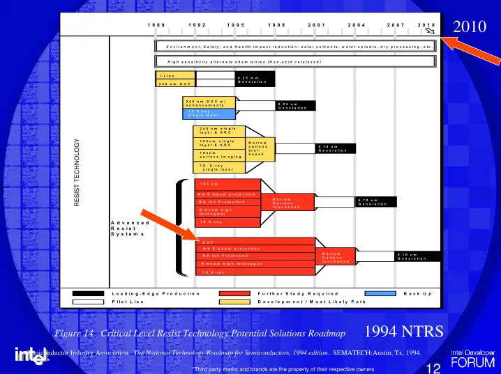
Figure 14 Critical Level Resist Technology Potential Solutions Roadmap
Semiconductor Industry Association.
The National Technology Roadmap for Semiconductors, 1994 edition
. SEMATECH:Austin, Tx, 1994.
1994 NTRS
EUV
F u r t h e r S t u d y R e q u i r e d L e a d i n g - E d g e P r o d u c t i o n
P i l o t L i n e D e v e l o p m e n t / M o s t L i k e l y P a t h
B a c k U p
2 0 0 4 1 9 9 2
1 9 8 9 1 9 9 5 1 9 9 8 2 0 0 1 2 0 0 7 2 0 1 0
E n v i r o n m e n t , S a f e t y , a n d H e a l t h i m p a c t r e d u c t i o n : s a f e r s o l v e n t s , w a t e r s o l u b l e , d r y p r o c e s s i n g , e t c .
H i g h s e n s i t i v i t y a l t e r n a t e c h e m i s t r i e s ( N o n - a c i d c a t a l y z e d )
0 . 3 5 m m G e n e r a t i o n
2 4 8 n m D U V I - L i n e
0 . 2 5 u m G e n e r a t i o n 1 X X - r a y
s i n g l e l a y e r
2 4 8 n m D U V w / e n h a n c e m e n t s
N a r r o w o p t i o n s t o o l -b a s e d
0 . 1 8 u m G e n e r a t i o n
2 4 8 n m s i n g l e l a y e r & A R C 1 9 3 n m s i n g l e l a y e r & A R C 1 X X - r a y s i n g l e l a y e r 1 9 3 n m s u r f a c e i m a g i n g N X I o n p r o j e c t i o n
E U V
1 X X - r a y
N a r r o w O p t i o n s t o o l - b a s e d N X E - b e a m p r o j e c t i o n
N X I o n P r o j e c t i o n E - b e a m h i g h t h r o u g p u t
0 . 1 0 u m G e n e r a t i o n N X E - b e a m p r o j e c t i o n
A d v a n c e d R e s i s t S y s t e m s
0 . 1 0 u m G e n e r a t i o n N a r r o w
O p t i o n s t o o l - b a s e d 1 9 3 n m
N X I o n P r o j e c t i o n E - b e a m h i g h t h r o u g p u t
1 X X - r a y
N X E - b e a m p r o j e c t i o n
13
*Third party marks and brands are the property of their respective owners
EUV Li thography i n
EUV Li thography i n
Commerci al Devel opment
Commerci al Devel opment
EUV Micro exposure tool (MET)
EUV Micro exposure tool (MET)
EUV MET Image (8/04)
EUV MET Image (8/04)
Integrated development in progress
Integrated development in progress
y
y
Source power and lifetime
Source power and lifetime
y
y
Defect free mask fabrication and handling
Defect free mask fabrication and handling
y
y
Optics lifetime
Optics lifetime
y
y
Resist performance
Resist performance
Source: Intel
14
*Third party marks and brands are the property of their respective owners
EUV Source Power Increased
EUV Source Power Increased
0.1
0.1
1
1
10
10
100
100
1000
1000
Jul
Jul-
-01
01
Jan-
Jan
-02
02
Jul-
Jul
-02
02
Jan-
Jan
-03
03
Jul-
Jul
-03
03
Jan-
Jan
-04
04
Jul-
Jul
-04
04
Jan-
Jan
-05
05
Jul
Jul-
-05
05
Jan-
Jan
-06
06
EUV Power at Intermediate Focus [W]EUV Power at Intermediate Focus [W]
115 W Production Requirement
115 W Production Requirement
Exponential fit to data
Exponential fit to data
Average of reported data
Average of reported data
(SEMATECH Source Workshops)
(SEMATECH Source Workshops)
Source: SEMATECH
15
*Third party marks and brands are the property of their respective owners
0.001
0.01
0.1
1
Jan-04
Apr-04
Jul-04
Sep-04
Dec-04
P
ro
c
ess ad
d
e
d
d
e
fect
d
e
n
s
it
y
@
80n
m
sen
s
it
iv
it
y (
c
m
-2)
EUV Mask Bl ank Defects Reduced
EUV Mask Bl ank Defects Reduced
Only 1 added
Only 1 added
defect!
defect!
Goal
Target for production @ 32nm
Target for production @ 32nm
Results from SEMATECH
Results from SEMATECH
Source: SEMATECH
16
*Third party marks and brands are the property of their respective owners
Cost/ Pi xel Trend w/ Tool Cost Ranges
(Source:
Intel ’03)
Cost/ Pi xel Trend w/ Tool Cost Ranges
Cost/ Pi xel Trend w/ Tool Cost Ranges
(Source:
(Source:
Intel
Intel
’
’
03)
03)
Cost/ Pi xel normal i zed to 90nm Node
Tool Cost Ranges based on 2002 ISMT Exposure Tool Cost Survey Resul ts
Cost/ Pi xel normal i zed to 90nm Node
Cost/ Pi xel normal i zed to 90nm Node
Tool Cost Ranges based on 2002 ISMT Exposure Tool Cost Survey Re
Tool Cost Ranges based on 2002 ISMT Exposure Tool Cost Survey Re
sul ts
sul ts
0.001
0.01
0.1
1
10
100
1990
1995
2000
2005
2010
2015
Normalized Cost/Pixel)
17
*Third party marks and brands are the property of their respective owners
Transistor Trade-offs
F
Max
= I
DSat
/ V
DD
C
ox
I
DSat
~1
µ
C
ox
(W)(V
DD
–V
T
)
2
2
Lg
Power= V
DD
2
C
ox
F
Max
S
D
G
Lg
W
Increase Cox
=>Reduce
t
ox
Reduce
Lg
Reduce
V
DD
ε
o
ε
s
18
*Third party marks and brands are the property of their respective owners
Gate Oxi de Scal i ng
Gate Oxi de Scal i ng
1
10
1990
1995
2000
2005
Gate Oxide
Thickness
(nm)
1
10
1.2 nm
90nm
.13um
.18um
.25um
.35um
Generation
I
DSat
1
µ
(V
DD
–V
T
)
2
2
Lg
W
ε
o
ε
s
1
t
ox
~
19
*T
h
ir
d
pa
rt
y
ma
rks
and
b
rand
s a
re
the p
rope
rty
o
f the
ir
r
e
spe
c
ti
ve
ow
ne
rs
Gate Delay Trend
100nm
F
Max
= I
DSat
/V
DD
C
ox
20
*Third party marks and brands are the property of their respective owners
Transi stor Performance
Transi stor Performance
0.0
0.2
0.4
0.6
0.8
1.0
1.2
1.4
1990
1995
2000
2005
Drive
Current
(mA/um)
1
10
Supply
Voltage
(V)
NMOS
PMOS
1.2V
90nm
.13um
.18um
.25um
.35um
Generation
I
DSat
1
µ
(V
DD
–V
T
)
2
2
Lg
W
ε
o
ε
s
1
t
ox
~
21
*Third party marks and brands are the property of their respective owners
The Incredible Shrinking
The Incredible Shrinking
Silicon Technology in the 90s
Silicon Technology in the 90s
0.35
0.35
µ
µ
Gate
Gate
Salicide
Salicide
Spacer
Spacer
Salicide
Salicide
1995
µ
µ
0.25
0.25
Salicide
Gate
Gate
Spacer
Spacer
Salicide
1997
0.18
0.18
µ
µ
Gate
Gate
Spacer
Spacer
Salicide
Salicide
1999
22
*Third party marks and brands are the property of their respective owners
New Transistor Trade-off
I
DSat
~1
µ
C
ox
(W)(V
DD
–V
T
)
2
2
Lg
S
D
G
Lg
W
Increase Cox
Reduce
Lg
µ
23
*Third party marks and brands are the property of their respective owners
Strai ned Si l i con Transi stors
Strai ned Si l i con Transi stors
Normal Silicon Lattice Strained Silicon Lattice
Current Flow
Normal
electron
flow
Faster
electron
24
*Third party marks and brands are the property of their respective owners
High
High
Stress
Stress
Film
Film
NMOS
NMOS
SiGe
SiGe
SiGe
SiGe
PMOS
PMOS
Compressive channel strain Tensile channel strain
30% drive current increase 10% drive current increase
Intel Produces Power Effi ci ent 90nm
Intel Produces Power Effi ci ent 90nm
Transi stors wi th Strai ned Si l i con
Transi stors wi th Strai ned Si l i con
Innovate and integrate
Innovate and integrate
for cost effective production
for cost effective production
Source: Intel
25
*Third party marks and brands are the property of their respective owners
65nm Technol ogy Hi ghl i ghts
65nm Technol ogy Hi ghl i ghts
y
y
Intel 65 nm generation logic technology provides
Intel 65 nm generation logic technology provides
improved performance and reduced power:
improved performance and reduced power:
–
–
1.2 nm transistor gate oxide
1.2 nm transistor gate oxide
–
–
35 nm transistor gate length
35 nm transistor gate length
–
–
Enhanced strained silicon technology
Enhanced strained silicon technology
–
–
8 layers of copper interconnect
8 layers of copper interconnect
–
–
Low
Low
-
-
k dielectric
k dielectric
y
y
This technology is being demonstrated on fully
This technology is being demonstrated on fully
functional 70
functional 70
Mbit
Mbit
SRAM chips with >0.5 billion
SRAM chips with >0.5 billion
transistors
transistors
y
y
Intel
Intel
’
’
s 65 nm technology is on track for delivery in
s 65 nm technology is on track for delivery in
2005
26
*Third party marks and brands are the property of their respective owners
Gate oxi de scal i ng has sl owed
Gate oxi de scal i ng has sl owed
Source: Intel
The power
challenge
I
DSat
1
µ
(V
DD
–V
T
)
2
2
Lg
W
ε
o
ε
s
1
t
ox
~
Mobi
lity
1
10
1990
1995
2000
2005
Gate Oxide
Thickness
(nm)
1
10
1.2 nm
0.5
µ
m
0.35
µ
m
0.25
µ
m
0.18
µ
m
0.13
µ
m
90nm
65nm
Slower scaling of one parameter can be
compensated by speeding up another
Tra
nsi
sto
r
per
for
27
*Third party marks and brands are the property of their respective owners
65nm Process
65nm Process
-
-
Transi stor
Transi stor
Strained silicon enhanced for
Strained silicon enhanced for
performance and power efficiency
performance and power efficiency
35nm
35nm
28
*Third party marks and brands are the property of their respective owners
65 nm Generati on Interconnects
65 nm Generati on Interconnects
M8
M7
M6
M5
M4
M3
M2
M1
• Metal 8 layer is added for
improved density and performance
(1 more layer than 90 nm generation)
• Low-k carbon doped oxide
dielectric reduces interconnect
capacitance
(improved from 90 nm
generation)
• Interconnect capacitance is
reduced by use of low-k dielectric
and by ~0.7x line length scaling
• Lower capacitance improves
interconnect performance and
reduces chip power
29
*Third party marks and brands are the property of their respective owners
130nm
130nm
90nm
65nm
200mm
300mm
300mm
300mm
2000
2001
2002
2003
2004
Defect
Density
(log scale)
Two Years
Defect Reducti on Trend
Defect Reducti on Trend
65 nm yield on same improvement rate with 2 years offset
30
*Third party marks and brands are the property of their respective ownersFul l y Functi onal Devi ces on Intel
Ful l y Functi onal Devi ces on Intel
’
’
s
s
65nm Process
65nm Process
Fully functional 70 Mbit SRAM
~110 mm
~110 mm
2
2
die size
die size
>0.5 billion transistors
>0.5 billion transistors
Yonah
31
*Third party marks and brands are the property of their respective ownersAgenda
Agenda
y
y
Moore
Moore
’
’
s Law and scaling
s Law and scaling
y
y
The power challenge
The power challenge
y
32
*Third party marks and brands are the property of their respective ownersPower Chal l enges
Power Chal l enges
y
y
Power challenges are neither new nor
Power challenges are neither new nor
fundamental
fundamental
–
–
“
“
Will it be possible to remove the heat generated by 10
Will it be possible to remove the heat generated by 10
’
’
s
s
of thousands of components?
of thousands of components?
”
”
(Moore, 1965)
(Moore, 1965)
–
–
Intel
Intel
’
’
s 1
s 1
st
st
product 1969: bipolar 3101 64
product 1969: bipolar 3101 64
-
-
b RAM
b RAM
y
y
Intel takes a holistic approach
Intel takes a holistic approach
–
–
From device/process power innovations
From device/process power innovations
–
–
Transistor optimization is a key to low
Transistor optimization is a key to low
-
-
power
power
–
–
To solutions at the platform level and beyond
To solutions at the platform level and beyond
y
y
Intel continues to invest and innovate on Moore
Intel continues to invest and innovate on Moore
’
’
s
s
Law
Law
–
–
R&D and capital
R&D and capital
–
–
Benefits to functions, performance/power, and cost
Benefits to functions, performance/power, and cost
33
*Third party marks and brands are the property of their respective ownersSi l i con Technol ogy Changes to
Si l i con Technol ogy Changes to
Increase Power Effi ci ency
Increase Power Effi ci ency
Mid
Mid
-
-
1960
1960
’
’
s: Bipolar, PMOS
s: Bipolar, PMOS
Mid
Mid
-
-
1970
1970
’
’
s: NMOS
s: NMOS
Mid
Mid
-
-
1980
1980
’
’
s: CMOS
s: CMOS
Mid
Mid
-
-
1990
1990
’
’
s: CMOS, Voltage scaling
s: CMOS, Voltage scaling
Mid
Mid
-
-
2000
2000
’
’
s: CMOS, Power efficient
s: CMOS, Power efficient
34
*Third party marks and brands are the property of their respective ownersSource: Intel, VLSI Technology Symposium 6/04
1
10
100
1000
0.2
0.4
0.6
0.8
1.0
1.2
1.4
1.6
Transistor
Transistor
Drive Current
Drive Current
(
(
mA
mA
/um)
/um)
Transistor
Leakage
Current
(nA/um)
Std
Strain
Std
Strain
+25% I
ON
+10% I
ON
0.04x I
OFF
0.20x I
OFF
PMOS
NMOS
15
15
90nm Strai ned Si l i con Saves
90nm Strai ned Si l i con Saves
Power @1.2V
Power @1.2V
5X to 25X reduction in transistor leakage power
35
*Third party marks and brands are the property of their respective owners65 nm Generati on Transi stors
65 nm Generati on Transi stors
y
y
1.2 nm gate oxide, 35 nm gate length for improved
1.2 nm gate oxide, 35 nm gate length for improved
performance
performance
y
y
220 nm contacted gate pitch for improved density
220 nm contacted gate pitch for improved density
y
y
NiSi for low resistance cap on gates and source
NiSi for low resistance cap on gates and source
-
-
drains
drains
y
y
Intel
Intel
’
’
s unique
s unique
uniaxial
uniaxial
strained silicon technology, first
strained silicon technology, first
introduced on the 90 nm generation, is further
introduced on the 90 nm generation, is further
enhanced on 65 nm transistors for improved
enhanced on 65 nm transistors for improved
performance
performance
y
y
At the 65 nm generation, strained silicon improves
At the 65 nm generation, strained silicon improves
performance ~30% relative to non
performance ~30% relative to non
-
-
strain
strain
36
*Third party marks and brands are the property of their respective owners1
10
100
1000
0.2
0.4
0.6
0.8
1.0
1.2
I
ON
(mA/um)
I
OFF
(nA/um)
PMOS
NMOS
90 nm
2002
2004
65 nm
2004
1.0 V
Improved Transi stor Performance
Improved Transi stor Performance
65 nm transistors increase drive current 10
65 nm transistors increase drive current 10
-
-
15% with
15% with
enhanced strain
37
*Third party marks and brands are the property of their respective owners1
10
100
1000
0.2
0.4
0.6
0.8
1.0
1.2
I
ON
(mA/um)
I
OFF
(nA/um)
PMOS
NMOS
90 nm
2002
2004
65 nm
2004
1.0 V
Improved Transi stor Performance
Improved Transi stor Performance
65 nm transistors can alternatively provide ~4x leakage
65 nm transistors can alternatively provide ~4x leakage
reduction
reduction
No other company has matched these performance
No other company has matched these performance
-
-
leakage
leakage
capabilities
capabilities
38
*Third party marks and brands are the property of their respective ownersStrai ned Si l i con
Strai ned Si l i con
y
y
Intel 90nm strain silicon has been in volume
Intel 90nm strain silicon has been in volume
production since 2003
production since 2003
y
y
Observed leakage reduction @1.2V
Observed leakage reduction @1.2V
–
–
N
N
-
-
Channel
Channel
-
-
> 5X Reduction
> 5X Reduction
–
–
P
P
-
-
Channel
Channel
-
-
> >5X Reduction
> >5X Reduction
y
y
Intel 65nm technology has been successfully
Intel 65nm technology has been successfully
demonstrated in 2004 using
demonstrated in 2004 using
“
“
2
2
nd
nd
Generation Strained
Generation Strained
Silicon
Silicon
”
”
y
y
Observed a further leakage reduction @1.0V from
Observed a further leakage reduction @1.0V from
90nm process
90nm process
–
–
N
N
-
-
Channel
Channel
-
-
> 4X Reduction
> 4X Reduction
–
–
P
P
-
-
Channel
Channel
-
-
> >4X Reduction
> >4X Reduction
39
*Third party marks and brands are the property of their respective ownersReduced Gate Capaci tance at 65nm
Reduced Gate Capaci tance at 65nm
Gate
Substrate
Source
Drain
C
GATE
Power
Saving
Feature
• Gate oxide thickness is held constant at
1.2 nm to avoid increased gate leakage
• Gate capacitance (C
GATE
) reduced ~20%
due to smaller gate length (35 nm)
• Lower gate capacitance reduces chip
active power
40
*Third party marks and brands are the property of their respective ownersGate
Substrate
Drain
Source
Oxide
C
WIRE
C
GATE
Gate
Substrate
Source
Drain
C
WIRE
C
JUNCT
C
GATE
Lower Juncti on Capaci tance
Lower Juncti on Capaci tance
Speeds up Ci rcui ts
Speeds up Ci rcui ts
(
1
- Cj/C total)
1
SOI reduces junction capacitance (under 5% of total),
but not gate or wire capacitance
41
*Third party marks and brands are the property of their respective ownersPlanar CMOS
Bulk CMOS vs. PDSOI
Gate
SiO
2
SiO
2
Silicon Substrate
Partially Depleted SOI
Gate
SiO
2
SiO
2
Silicon Substrate
Buried Oxide
Silicon Substrate
42
*Third party marks and brands are the property of their respective ownersIntel Already Has the Lowest Junction
Intel Already Has the Lowest Junction
Capacitance (180nm data)
Capacitance (180nm data)
S. Tyagi, IEDM 2000
Intel achieves the industry’s lowest junction capacitance
without SOI, thereby avoiding the cost of SOI
The power
challenge
Intel
0.40
0.60
0.80
1.00
1.20
1.40
1.60
-0.5
0
0.5
1
1.5
Bias (V)
N+/PWell
P+/Nwell
Wang, EDL Oct.'00
Mehrotra IEDM '99
Imai, IEDM '99
Yoshimura, VLSI '00
Diaz, VLSI '00
Yeap, VLSI '00
Junction
Capacitance
43
*Third party marks and brands are the property of their respective owners• All 3 elements of SOI performance diminish with scaling
- Gain for 90nm node: 3-10% depending on history guardband
0.18um
130nm
90nm
F.O.=1 Inverter
16%
13%
11%
F.O.=4 Inverter
8%
7%
6%
3-Input NAND
20%
17%
14%
Average
15%
12%
10%
History Guardband
-5%
-6%
-7%
NET
10%
6%
3%
Analysis ignores interconnect load, which reduces SOI gain further
K. Mistry, VLSI 2000
Net Impact of SOI Goes Down wi th
Net Impact of SOI Goes Down wi th
Each Generati on
Each Generati on
44
*Third party marks and brands are the property of their respective ownersIntel
Intel
’
’
s bul k CMOS has extremel y l ow
s bul k CMOS has extremel y l ow
Cj
Cj
y
y
Low
Low
Cj
Cj
=~ 0.1 x C total
=~ 0.1 x C total
y
y
Gross performance
Gross performance
gain = 1/(1
gain = 1/(1
-
-
0.1) =
0.1) =
11%
11%
y
y
Net gain is low
Net gain is low
y
y
Bulk substrate cost
Bulk substrate cost
much less
much less
y
y
If
If
Cj
Cj
= ~0.25 x C total
= ~0.25 x C total
y
y
Then, gross performance
Then, gross performance
gain = 1/(1
gain = 1/(1
–
–
0.25) =
0.25) =
33%
33%
y
y
Net gain is high
Net gain is high
y
y
High
High
Cj
Cj
is indicative of an
is indicative of an
under optimized bulk
under optimized bulk
CMOS process
CMOS process
(
1
- Cj/C total)
1
45
*Third party marks and brands are the property of their respective ownersSi Substrate
Si Substrate
Oxide
R
SD
R
JUNCT
R
GATE
BULK SOI
SOI reduces junction capacitance, but not gate or wire capacitance
Has SOI “solved” the leakage problem? “No”
• SOI eliminated junction leakage
• Junction leakage is < 5% of total leakage in Intel process
• Ioff of Intel Strained Silicon is >10x lower than any reported data,
Including SOI
R
GATE
46
*Third party marks and brands are the property of their respective ownersSummary of Strai ned Si l i con vs. SOI
Summary of Strai ned Si l i con vs. SOI
y
y
Intel 90nm strain silicon has been in volume
Intel 90nm strain silicon has been in volume
production since 2003
production since 2003
y
y
Partially depleted (PD)
Partially depleted (PD)
-
-
SOI has no place on Intel
SOI has no place on Intel
roadmap:
roadmap:
–
–
Intel has thoroughly evaluated costs/benefits
Intel has thoroughly evaluated costs/benefits
–
–
Is saving millions per year on substrate alone by avoiding SOI
Is saving millions per year on substrate alone by avoiding SOI
–
–
Cost adder is 15% or more
Cost adder is 15% or more
–
–
Performance benefit is less than 5% at 90nm
Performance benefit is less than 5% at 90nm
y
y
Intel demonstrated transistors with world
Intel demonstrated transistors with world
-
-
leading
leading
performance/leakage characteristics:
performance/leakage characteristics:
–
–
Low
Low
-
-
junction
junction
-
-
capacitance bulk CMOS at 130nm
capacitance bulk CMOS at 130nm
–
–
Uniaxial strained silicon at 90nm and beyond
Uniaxial strained silicon at 90nm and beyond
y
y
Fully depleted (FD)
Fully depleted (FD)
-
-
SOI (e.g. Tri
SOI (e.g. Tri
-
-
gate) has been under
gate) has been under
evaluation for future:
evaluation for future:
–
–
Final decision depends on costs/benefits
Final decision depends on costs/benefits
47
*Third party marks and brands are the property of their respective ownersSl eep Transi stors Reduce Leakage
Sl eep Transi stors Reduce Leakage
Power
Power
70
70
Mbit
Mbit
SRAM IR photos
SRAM IR photos
>3x SRAM leakage
>3x SRAM leakage
reduction with use of
reduction with use of
sleep transistors
sleep transistors
Normal SRAM
Normal SRAM
sub
sub
-
-
block leakage
block leakage
Sleep transistors
Sleep transistors
shut off leakage in
shut off leakage in
inactive sub
inactive sub
-
-
blocks
blocks
Power
Saving
Feature
V
V
SS
SS
V
V
DD
DD
NMOS
NMOS
Sleep
Sleep
Transistor
Transistor
48
*Third party marks and brands are the property of their respective owners87 mm
87 mm
2
2
83 mm
83 mm
2
2
Die size
Die size
21 W
21 W
24.5 W
24.5 W
Thermal design power
Thermal design power
2 MB
2 MB
1 MB
1 MB
L2 cache
L2 cache
140 million
140 million
77 million
77 million
Transistors
Transistors
2.1 GHz
2.1 GHz
1.7 GHz
1.7 GHz
Frequency
Frequency
90 nm
90 nm
(Dothan)
(Dothan)
130 nm
130 nm
(Banias)
(Banias)
Pentium
Pentium
®
®
M processor
M processor
Si l i con Scal i ng Conti nues to Improve
Si l i con Scal i ng Conti nues to Improve
Densi ty, Performance, Power, Cost
Densi ty, Performance, Power, Cost
Mobi l e CPUs
Mobi l e CPUs
The power
challenge
49
*Third party marks and brands are the property of their respective ownersSl eep Transi stors
Sl eep Transi stors
Reduce ALU Leakage
Reduce ALU Leakage
Scan
FIFO
Scan
out
Sleep
ALU
Body bias
Control
37X leakage reduction
37X leakage reduction
demonstrated on test chip
demonstrated on test chip
Scan
Scan
PMOS
PMOS underdrive
underdrive
V
V
ccccPMOS overdrive
PMOS overdrive V
V
ssssVirtual
Virtual V
V
ccccVirtual
Virtual V
V
ssssScan
Scan
capture
capture
control
control
Dynamic
Dynamic
ALU
ALU
3232NMOS overdrive
NMOS overdrive V
V
ccccNMOS
NMOS underdrive
underdrive
V
V
ssssALU core
ALU core
3
3-
-bit A/D
bit A/D
ALU
ALU
Body
Body
Bias
Bias
PMOS
PMOS
Sleep
Sleep
Body
Body
Bias
Bias
V
V
ss
ss
external
external
V
V
cc
cc
external
external
Sleep transistor
Sleep transistor
and body bias
and body bias
control
control
Sleep transistors
Sleep transistors
Source: ISSCC 2003, Paper 6.1
50
*Third party marks and brands are the property of their respective ownersAdvances i n Power Effi ci ent Desi gn
Advances i n Power Effi ci ent Desi gn
0
50
100
150
200
250
300
350
Cache Switch
Cache Igate
Cache Ioff
Core Switch
Core Igate
Core Ioff
IO bias
DCAP lkg
Using
Using
prior
prior
design
design
techniques
techniques
With new
With new
power
power
reduction
reduction
techniques
techniques
From ISSCC 2005
From ISSCC 2005
Paper 10.1
Paper 10.1
“
“
The Implementation of
The Implementation of
a 2
a 2
-
-
core Multi
core Multi
-
-
Threaded
Threaded
Itanium
Itanium
TM
TM
Family
Family
Processor
Processor
”
”
Power
Power
(W)
(W)
51
*Third party marks and brands are the property of their respective owners1.72 Billion
transistors
21.5 mm
27.72 mm
Business Critical Features
1MB L2I
2-Way
Multi-Threading
Foxton
Power
Controller
2 X 12MB L3
Caches with
Pellston
Soft Error Detection
and Correction
Dual
52
*Third party marks and brands are the property of their respective ownersSi l i con Scal i ng Conti nues to Improve
Si l i con Scal i ng Conti nues to Improve
Densi ty, Performance, Power, Cost
Densi ty, Performance, Power, Cost
Server CPUs
Server CPUs
130 nm 90 nm
130 nm 90 nm
Madison
Madison
Montecito
Montecito
Cores/Threads
Cores/Threads
1/1
1/1
2/4
2/4
Transistors
Transistors
0.41
0.41
1.72
1.72
Billion
Billion
L3 Cache
L3 Cache
6
6
24
24
MByte
MByte
Frequency
Frequency
1.5
1.5
>1.7
>1.7
GHz
GHz
Relative Performance
Relative Performance
1
1
>1.5x
>1.5x
Thermal Design Power
Thermal Design Power
130
130
~100
~100
Watt
Watt
The power
challenge
53
*Third party marks and brands are the property of their respective ownersDual Core
Dual Core
Core
Cache
Core
Cache
Core
Voltage = 1
Freq = 1
Power = 1
Perf
= 1
Voltage = -15%
Freq = -15%
Power = 1
Perf
= ~1.8
The power challenge
54
*Third party marks and brands are the property of their respective ownersMul ti
Mul ti
-
-
Core
Core
C1
C2
C3
C4
Cache
Large Core
Cache
1
2
3
4
1
2
Small
Core
1
1
1
2
3
4
1
2
3
4
Power
Performance
Power = 1/4
Performance = 1/2
Multi
Multi
-
-
Core:
Core:
Power efficient
Power efficient
Better power and
Better power and
thermal management
thermal management
55
*Third party marks and brands are the property of their respective ownersPerformance and Power Effi ci ency
Performance and Power Effi ci ency
Increase wi th Paral l el Archi tecture
Increase wi th Paral l el Archi tecture
FORECAST
FORECAST
DUAL/MULTI
DUAL/MULTI
-
-
CORE
CORE
2000
2000
2008+
2008+
Relative
Relative
processor
processor
performance*
performance*
(constant
(constant
power
power
envelope)
envelope)
2004
2004
SINGLE
SINGLE
-
-
CORE
CORE
10X
10X
*Average of SPECInt2000 and SPECFP2000 rates for Intel desktop
*Average of SPECInt2000 and SPECFP2000 rates for Intel desktop processors
processors
vs
vs
initial Intel
initial Intel
®®Pentium
Pentium
®®4 Processor
4 Processor
Source: Intel
3X
3X
The power
challenge
56
*Third party marks and brands are the property of their respective ownersAgenda
Agenda
y
y
Moore
Moore
’
’
s Law and scaling
s Law and scaling
y
y
The power challenge
The power challenge
y
57
*Third party marks and brands are the property of their respective ownersFuture Hi gh
Future Hi gh
-
-
k Di el ectri c
k Di el ectri c
Wi l l Reduce Gate Leakage
Wi l l Reduce Gate Leakage
Silicon substrate
Gate
3.0nm High-k
Silicon substrate
1.2nm SiO
2
Gate
L
L
ower
ower
power
power
> 100x reduction
> 100x reduction
Gate dielectric
Gate dielectric
leakage
leakage
Faster transistors
Faster transistors
60% greater
60% greater
Gate capacitance
Gate capacitance
Benefit
Benefit
High
High
-
-
k vs. SiO
k vs. SiO
2
2
Fo
r F
utu
re
Im
ple
me
nta
tio
n
Fo
r F
utu
re
Im
ple
me
nta
58
*Third party marks and brands are the property of their respective ownersGate Di el ectri c Scal i ng (Hi gh
Gate Di el ectri c Scal i ng (Hi gh
-
-
K)
K)
1
10
1990
1995
2000
2005
Gate Dielectric
Thickness
(nm)
1
10
1.2 nm
Thinner equivalent gate oxide increases transistor performance
Thinner equivalent gate oxide increases transistor performance
90nm
.13um
.18um
.25um
.35um
Generation
2010
K=
3
X
K
D
K=
5
X
K
59
*Third party marks and brands are the property of their respective ownersConti nuati on of Moore
Conti nuati on of Moore
’
’
s Law
s Law
Strained
Strained
Si
Si
Strained Si
Strained Si
Strained
Strained
Si
Si
Strained
Strained
Si
Si
Strained
Strained
Si
Si
Si
Si
Si
Si
Si
Si
Channel
Channel
P1270
P1270
P1268
P1268
P1266
P1266
P1264
P1264
P1262
P1262
Px60
Px60
P858
P858
P856
P856
Process Name
Process Name
300
300
300
300
300
300
300
300
300
300
200/300
200/300
200
200
200
200
Wafer Size (mm)
Wafer Size (mm)
Metal
Metal
Metal
Metal
Metal
Metal
Poly
Poly
-
-silicon
silicon
Poly
Poly
-
-silicon
silicon
Poly
Poly
-
-silicon
silicon
Poly
Poly
-
-silicon
silicon
Poly
Poly
-
-silicon
silicon
Gate electrode
Gate electrode
High
High
-
-
k
k
High
High
-
-
k
k
High
High
-
-
k
k
SiO
SiO
2
2
SiO
SiO
2
2
SiO
SiO
2
2
SiO
SiO
2
2
SiO
SiO
2
2
Gate dielectric
Gate dielectric
?
?
Cu
Cu
Cu
Cu
Cu
Cu
Cu
Cu
Cu
Cu
Al
Al
Al
Al
Inter
Inter
-
-
connect
connect
22 nm
22 nm
32 nm
32 nm
45 nm
45 nm
65 nm
65 nm
90 nm
90 nm
0.13
0.13
µm
µ
m
0.18
0.18
µm
µ
m
0.25
0.25
µm
µ
m
Process
Process
Generation
Generation
2011
2011
2009
2009
2007
2007
2005
2005
2003
2003
2001
2001
1999
1999
1997
1997
1st Production
1st Production
Potential candidate for introduction
Potential candidate for introduction
Subject to change
Subject to change
Intel found a solution for
High-k
and metal gate
Intel found a solution for
Intel found a solution for
High
High
-
-
k
k
and metal gate
and metal gate
60
*Third party marks and brands are the property of their respective ownersy
y
Structures measured in nanometers
Structures measured in nanometers
–
–
Less than 0.1
Less than 0.1
-
-
micron (100nm)
micron (100nm)
y
y
New processes, materials, device structures
New processes, materials, device structures
–
–
Incrementally changing silicon technology base
Incrementally changing silicon technology base
y
y
Materials manipulated on atomic scale
Materials manipulated on atomic scale
–
–
In one or more dimensions
In one or more dimensions
y
y
Increasing use of self
Increasing use of self
-
-
assembly
assembly
–
–
Using chemical properties to form structures
Using chemical properties to form structures
Nanotechnology innovations will extend
Nanotechnology innovations will extend
silicon technology and Moore
silicon technology and Moore
’
’
s Law
s Law
Nanotechnol ogy Hal l marks
Nanotechnol ogy Hal l marks
61
*Third party marks and brands are the property of their respective ownersBOX
Source
Drain Source
Gate
Drain Si fin - Body!
FinFET
Surroundi ng the Semi conductor
Surroundi ng the Semi conductor
Drain
Source
Metal
Gate Insulator
Source
Drain
Gate
62
*Third party marks and brands are the property of their respective ownersTri-Gate
Planar CMOS
Tri-gate Transistor works in
Three Dimensions
Gate 2
Gate 3
Gate 1
Buried Oxide
Gate
SiO
2
SiO
2
63
*Third party marks and brands are the property of their respective ownersSi
T
Si
L
g
Si
T
Planar fully depleted SOI
Double-gate (e.g. FINFET)
W
Si
L
g
T
Si
Isolation
(Non-Planar)
(Planar)
W
Si
L
g
T
Si
Tri-gate
(Non-Planar)
Most
Manufacturable
New Devi ce Archi tecture
New Devi ce Archi tecture
Tri
64
*Third party marks and brands are the property of their respective ownersTri
Tri
-
-
Gate Transi stor:
Gate Transi stor:
“
“
A templ ate for the future
A templ ate for the future
”
”
SOURCE
DRAIN
GATE
Technical details presented at:
Technical details presented at:
ISSDM Conference, Japan, Sept 17, 2002
ISSDM Conference, Japan, Sept 17, 2002
Source: Intel
SOURCE
DRAIN
65
*Third party marks and brands are the property of their respective ownersNano
Nano
-
-
Devi ce Structure Evol uti on
Devi ce Structure Evol uti on
Tri-gate Transistor
Gate
Fully-Surround Gate
Transistor
Best Electrostatics
and Scalability
Improved
Electrostatics
SiO2
Gate
SiO2
Conventional Planar Transistor
66
*Third party marks and brands are the property of their respective owners5 nm Si
Nanowire
Metal Gate
2.0 nm
High-K
Semi conductor Nanowi res
Semi conductor Nanowi res
Chemically synthesized
silicon nanowires with
diameters <20nm (not
defined by lithography).
Si Nanowire
67
*Third party marks and brands are the property of their respective ownersCarbon Nanotube Tutori al
Carbon Nanotube Tutori al
y
y
Rolled
Rolled
-
-
up graphene sheet(s)
up graphene sheet(s)
y
y
Roll
Roll
-
-
up vector determines
up vector determines
electronic properties of tubes
electronic properties of tubes
–
–
metallic
metallic
–
–
semiconducting
semiconducting
y
y
Dimensions:
Dimensions:
1
1
-
-
25nm depending on how they
25nm depending on how they
are form.
are form.
Semi-conductor
Metal
R
r
68
*Third party marks and brands are the property of their respective ownersCarbon Nanotube Transi stor
Carbon Nanotube Transi stor
Source
Carbon
Nanotube
-D = 1.4 nm
Gate
Drain
L
g
= 75 nm
Chemically synthesized
semiconducting
nanotubes with
diameter=2nm
form the transistor
channel.
69
*Third party marks and brands are the property of their respective ownersEnergy
Energy
-
-
del ay product for PMOS
del ay product for PMOS
70
*Third party marks and brands are the property of their respective ownersCompound Semi conductor (
Compound Semi conductor (
l l l
l l l
-
-
V)
V)
Transi stors
Transi stors
Gate
Drain
Source
Source
Multi
epitaxial
layers
Research transistor based
on multi-epitaxial layer
structure in compound
semiconductors.
So u r ce : I n t e l
71
*Third party marks and brands are the property of their respective ownersIII/V is a 2015 Transistor option
•
3x faster or 10x lower power
•
Integration with silicon key
CMOS to conti nue for 15
CMOS to conti nue for 15
-
-
20 years or more;
20 years or more;
Moore
Moore
’
’
s Law coul d be extended i ndefi ni tel y vi a new
s Law coul d be extended i ndefi ni tel y vi a new
archi tectures, heterogeneous i ntegrati on, 3D
archi tectures, heterogeneous i ntegrati on, 3D
0.2um InSb
0.2um NMOS
Po
w
e
r
C
o
nsum
pt
io
n
0.2um InSb
0.2um NMOS
T
ra
n
si
st
o
r
Sp
e
e
d
72
*Third party marks and brands are the property of their respective ownersEnergy
Energy
-
-
del ay product for NMOS
del ay product for NMOS
73
*Third party marks and brands are the property of their respective ownersTransistor Scaling
Transistor Scaling
& Roadmap
& Roadmap
LG= 10nm
LG= 10nm
20nm Length
(Development)
25 nm
15nm
15nm Length
15nm Length
(Research)
(Research)
65nm Node
P1264
2005
45nm Node
P1266
2007
90nm Node
2003
32nm Node
P1268
2009
22nm Node
P1270
2011
10nm Length
10nm Length
(Research)
(Research)
C
C
-
-
nanotube
nanotube
Prototype
Prototype
(Research)
(Research)
Nanowire
Nanowire
Prototype
Prototype
(Research)
(Research)
5 n m 5 n m
74
*Third party marks and brands are the property of their respective ownersMoore
Moore
’
’
s Law Today
s Law Today
Moore’s Law
y
y
Moore
Moore
’
’
s Law = Doubling of
s Law = Doubling of
components at fixed intervals while
components at fixed intervals while
reducing production
reducing production
cost/component
cost/component
y
y
Moore's Law is alive and well
Moore's Law is alive and well
y
y
CMOS has been an important
CMOS has been an important
enabler of Moore
enabler of Moore
’
’
s Law
s Law
y
y
Moore's Law may go on indefinitely,
Moore's Law may go on indefinitely,
and extend beyond traditional CMOS
and extend beyond traditional CMOS
y
y
“
“
End of CMOS Scaling
End of CMOS Scaling
”
”
≠
≠
“
“
End of
End of
Moore
75
*Third party marks and brands are the property of their respective ownersBipolar
Bipolar
Moore
Moore
’
’