I. INT
RODUCTION
Contents
I.1 Introduction
I.2 Analog Integrated Circuit Design I.3 Technology Overview
I.4 Notation
Organization
DEVICES SYSTEMS
CIRCUITS
Chapter 2 CMOS Technology
Chapter 3 CMOS Device
Modeling
Chapter 4 Device Characterization Chapter 7
CMOS Comparators
Chapter 8 Simple CMOS
Opamps
Chapter 9 High Performance
Opamps
Chapter 5 CMOS Subcircuits
Chapter 6 CMOS Amplifiers Chapter 10
D/A and A/D Converters
Chapter 11 Analog Systems
SIMPLE COMPLEX
I.1 - INTRODUCTION
GLOBAL OBJECTIVES
• Teach the analysis, modeling, simulation, and design of analog circuits implemented in CMOS technology.
• Emphasis will be on the design methodology and a hierarchical approach to the subject.
SPECIFIC OBJECTIVES
1. Present an overall, uniform viewpoint of CMOS analog circuit design. 2. Achieve an understanding of analog circuit design.
• Hand calculations using simple models • Emphasis on insight
• Simulation to provide second-order design resolution 3. Present a hierarchical approach.
I.2 ANALOG INTEGRATED CIRCUIT DESIGN
ANALOG DESIGN TECHNIQUES VERSUS TIME
Requires precise definition of time constants (RC
products)
FILTERS AMPLIFICATION
Passive RLC circuits Open-loop amplifiers
Active-RC Filters Feedback Amplifiers Requires precise definition
of passive components
Switched Capacitor Filters
Requires precise C ratios and clock
Switched Capacitor Amplifiers Requires precise C
ratios
Continuous Time Filters Time constants are
adjustable
Continuous Time Amplifiers Component ratios
are adjustable 1978
1983 1935-1950
1992
DISCRETE VS. INTEGRATED ANALOG CIRCUIT DESIGN
Activity/Item Discrete Integrated
Component Accuracy Well known Poor absolute accuracies
Breadboarding? Yes No (kit parts)
Fabrication Independent Very Dependent
Physical
Implementation
PC layout Layout, verification, and extraction
Parasitics Not Important Must be included in the
design Simulation Model parameters well
known
Model parameters vary widely
Testing Generally complete
testing is possible
Must be considered before the design
CAD Schematic capture,
simulation, PC board layout
Schematic capture, simulation, extraction, LVS, layout and routing
Components All possible Active devices,
THE ANALOG IC DESIGN PROCESS
Conception of the idea
Definition of the design
Implementation
Simulation
Physical Verification
Parasitic Extraction
Fabrication
Testing and Verification
Product Comparison
with design specifications
Comparison with design specifications
COMPARISON OF ANALOG AND DIGITAL CIRCUITS
Analog Circuits Digital Circuits
Signals are continuous in amplitude and can be continuous or discrete in time
Signal are discontinuous in amplitude and time - binary signals have two amplitude states
Designed at the circuit level Designed at the systems level Components must have a continuum
of values Component have fixed values
Customized Standard
CAD tools are difficult to apply CAD tools have been extremely successful
Requires precision modeling Timing models only
Performance optimized Programmable by software
Irregular block Regular blocks
Difficult to route automatically Easy to route automatically Dynamic range limited by power
I.3 TECHNOLOGY OVERVIEW
BANDWIDTHS OF SIGNALS USED IN SIGNAL PROCESSING APPLICATIONS
10
1 100 1k 10k 100k 1M 10M 100M 1G 10G 100G Seismic
Sonar
Audio
Video Acoustic imaging
Radar
AM-FM radio, TV
Telecommunications Microwave
Signal Frequency (Hz)
BANDWIDTHS THAT CAN BE PROCESSED BY PRESENT-DAY TECHNOLOGIES
Frequencies that can be processed by present-day technologies. 10
1 100 1k 10k 100k 1M 10M 100M 1G 10G 100G Signal Frequency (Hz)
GaAs
Optical MOS digital logic
Bipolar digital logic Bipolar analog
CLASSIFICATION OF SILICON TECHNOLOGY
Silicon IC Technologies
Bipolar Bipolar/MOS MOS
Junction
Isolated Dielectric Isolated CMOS (Aluminum PMOS Gate)
NMOS
Aluminum
BIPOLAR VS. MOS TRANSISTORS
CATEGORY BIPOLAR CMOS
Turn-on Voltage 0.5-0.6 V 0.8-1 V
Saturation Voltage 0.2-0.3 V 0.2-0.8 V
gm at 100µA 4 mS 0.4 mS (W=10L)
Analog Switch
Implementation Offsets, asymmetric Good
Power Dissipation Moderate to high Low but can be large
Speed Faster Fast
Compatible Capacitors Voltage dependent Good AC Performance
Dependence DC variables only DC variables andgeometry
Number of Terminals 3 4
Noise (1/f) Good Poor
Noise Thermal OK OK
WHY CMOS???
CMOS is nearly ideal for mixed-signal designs: • Dense digital logic
• High-performance analog
DIGITAL ANALOG
I.4 NOTATION
SYMBOLS FOR TRANSISTORS
Drain Gate
Source/bulk Drain
Gate
Source
Bulk
n-channel, enhance-ment, VBS ≠ 0
n-channel, enhance-ment, bulk at most negative supply
Drain Gate
Source/bulk Drain
Gate
Source
Bulk
p-channel, enhance-ment, VBS ≠ 0
SYMBOLS FOR CIRCUIT ELEMENTS
+
-A V
+
-G V
R I I
A I +
-m 1 1
V1
v 1
I1
V1
m 1
i 1
V I
Operational Amplifier/Amplifier/OTA
VCVS VCCS
Notation for signals
ID
Id
id
iD
II. CMOS TECHNOLOGY
Contents
II.1 Basic Fabrication Processes II.2 CMOS Technology
II.3 PN Junction II.4 MOS Transistor II.5 Passive Components II.6 Latchup Protection II.7 ESD Protection
Perspective
DEVICES SYSTEMS
CIRCUITS
Chapter 2 CMOS Technology
Chapter 3 CMOS Device
Modeling
Chapter 4 Device Characterization Chapter 7
CMOS Comparators
Chapter 8 Simple CMOS
Opamps
Chapter 9 High Performance
Opamps
Chapter 5 CMOS Subcircuits
Chapter 6 CMOS Amplifiers Chapter 10
D/A and A/D Converters
Chapter 11 Analog Systems
OBJECTIVE
• Provide an understanding of CMOS technology sufficient to enhance circuit design.
• Characterize passive components compatible with basic technologies. • Provide a background for modeling at the circuit level.
II.1 - BASIC FABRICATION PROCESSES
BASIC FABRTICATION PROCESSES
Basic Steps
• Oxide growth • Thermal diffusion • Ion implantation • Deposition • Etching
Photolithography
Means by which the above steps are applied to selected areas of the silicon wafer.
Silicon wafer
0.5-0.8 mm
125-200 mm
Oxidation
The process of growing a layer of silicon dioxide (SiO2)on the surface of a silicon wafer.
Original Si surface
0.44 tox
tox
Si substrate SiO2
Uses:
• Provide isolation between two layers
• Protect underlying material from contamination
Diffusion
Movement of impurity atoms at the surface of the silicon into the bulk of the silicon - from higher concentration to lower concentration.
Low Concentration High
Concentration
Diffusion typically done at high temperatures: 800 to 1400 °C. Infinite-source diffusion:
N(x)
Depth (x) ERFC
t1<t2<t3
t1 t2 t3
NB N0
Finite-source diffusion:
Depth (x)
t1<t2<t3
t1 t2 t3
Gaussian
Ion Implantation
Ion implantation is the process by which impurity ions are accelerated to a high velocity and physically lodged into the target.
Fixed atoms Path of impurity atom
Impurity final resting place
• Anneal required to activate the impurity atoms and repair physical damage to the crystal lattice. This step is done at 500 to 800 °C. • Lower temperature process compared to diffusion.
• Can implant through surface layers, thus it is useful for field-threshold adjustment.
• Unique doping provile available with buried concentration peak.
N(x)
N
Depth (x) 0
Concentration peak
Deposition
Deposition is the means by which various materials are deposited on the silicon wafer.
Examples:
• Silicon nitride (Si3N4) • Silicon dioxide (SiO2) • Aluminum
• Polysilicon
There are various ways to deposit a meterial on a substrate: • Chemical-vapor deposition (CVD)
• Low-pressure chemical-vapor deposition (LPCVD) • Plasma-assisted chemical-vapor deposition (PECVD) • Sputter deposition
Etching
Etching is the process of selectively removing a layer of material. When etching is performed, the etchant may remove portions or all of: • the desired material
• the underlying layer • the masking layer Important considerations: • Anisotropy of the etch
A = 1 - vertical etch ratelateral etch rate
• Selectivity of the etch (film toomask, and film to substrate) Sfilm-mask = mask etch ratefilm etch rate
Desire perfect anisotropy (A=1) and invinite selectivity. There are basically two types of etches:
• Wet etch, uses chemicals
• Dry etch, uses chemically active ionized gasses.
Mask Film
b
Underlying layer a
Photolithography
Components
• Photoresist material • Photomask
• Material to be patterned (e.g., SiO2) Positive
photoresist-Areas exposed to UV light are soluble in the developer Negative
photoresist-Areas not exposed to UV light are soluble in the developer Steps:
1. Apply photoresist 2. Soft bake
3. Expose the photoresist to UV light through photomask 4. Develop (remove unwanted photoresist)
5. Hard bake
Photoresist
Photomask UV
Light
Photomask
Positive Photoresist Photoresist
Photoresist
Polysilicon
Polysilicon
II.2 - CMOS TECHNOLOGY
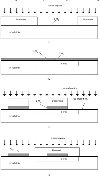
TWIN-WELL CMOS TECHNOLOGY
Features
• Two layers of metal connections, both of them of high quality due to a planarization step.
n-well implant
Photoresist Photoresist
(a)
Photoresist p- field implant
Si3N4
(d)
n-well (b)
Si3N4
n-well
Photoresist
Photoresist
n- field implant
Pad oxide (SiO2)
(c)
n-well Si3N4
Figure 2.1-5 The major CMOS process steps. p- substrate
p- substrate
p- substrate
p- substrate
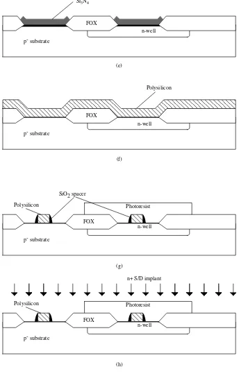
SiO2
Photoresist SiO2 spacer
Polysilicon
FOX FOX
Polysilicon
n-well
FOX
(e)
(f)
(g)
n-well
n-well Si3N4
Figure 2.1-5 The major CMOS process steps (cont'd).
p- substrate
p- substrate
p- substrate
FOX
FOX
FOX
Photoresist n+ S/D implant
Polysilicon
FOX
(h)
n-well
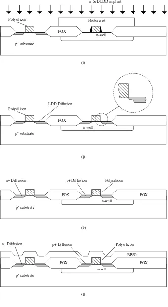
p- substrate
BPSG Polysilicon n+ Diffusion p+ Diffusion
FOX FOX
(l)
Figure 2.1-5 The major CMOS process steps (cont'd).
n-well Polysilicon
n-well n+ Diffusion p+ Diffusion
FOX FOX
(k)
p- substrate p- substrate
(j)
Photoresist n- S/D LDD implant
Polysilicon
FOX
(i)
n-well
p- substrate
FOX
Polysilicon
FOX
n-well p- substrate
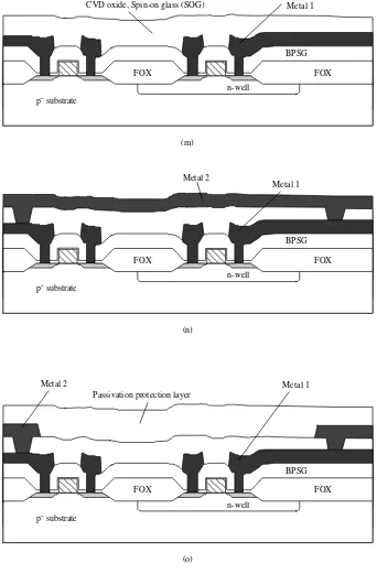
Figure 2.1-5 The major CMOS process steps (cont'd).
(m)
BPSG
n-well
FOX FOX
p- substrate
BPSG
n-well
Metal 1
FOX FOX
p- substrate
(n)
(o) Metal 2
BPSG
n-well
Metal 1
FOX FOX
p- substrate Metal 2
Metal 1 CVD oxide, Spin-on glass (SOG)
Silicide/Salicide
Purpose
• Reduce interconnect resistance,
Figure 2.1-6 (a) Polycice structure and (b) Salicide structure. (a)
Metal
FOX
(b)
FOX
Polysilicide Polysilicide
II.3 - PN JUNCTION
CONCEPT
Metallurgical Junction p-type semiconductor n-type semiconductor
iD
+ -vD Depletion region
x
p-type semicon-ductor
n-type semicon-ductor
iD
+ -vD
xd
xp 0 xn
1. Doped atoms near the metallurgical junction lose their free carriers by diffusion.
2. As these fixed atoms lose their free carriers, they build up an electric field which opposes the diffusion mechanism.
3. Equilibrium conditions are reached when:
PN JUNCTION CHARACTERIZATION
ND
-NA
x 0
Impurity concentration ( cm-3)
x 0
Depletion charge concentration ( cm-3)
qND
-qNA
xp
xn
Electric Field (V/cm)
Eo
x
x Potential (V)
xd
φ − o Dv
p-type
semi- con-ductor
n-type semi- con-ductor
iD
+vD -xd
xn
SUMMARY OF PN JUNCTION ANALYSIS
Barrier
potential-φo = kTq lnNnAND
i2 = Vt ln
NAND
ni2 Depletion region
widths-
xn = 2εqNsi(φo-vD)NA D(NA+ND)
xp = 2εqNsi(φo-vD)ND
D(NA+ND)
x ∝ N 1
Depletion
capacitance-Cj = A 2(NεsiqNAND
A+ND)
1 φo-vD
= Cj0 φo-vD
Breakdown
voltage-BV = εsi2qN(NA+ND)
AND E
SUMMARY - CONTINUED
Current-Voltage Relationship-iD = Is
exp vD
Vt - 1 where Is = qA
Dppno Lp +
Dnnp o Ln
-40 -30 -20 -10 0 10 20 30 40 vD/Vt
iD Is 10 8 6 4 2 0 x1016 x1016 x1016 x1016 x1016 -5 0 5 10 15 20 25
-4 -3 -2 -1 0 1 2 3 4
iD
Is
II.4 - MOS TRANSISTOR
ILLUSTRATION
Fig. 4.3-4
n+ n+
p-substrate (bulk)
Channel Length, L n-channel
Polysilicon
Bulk Source Gate Drain
p+
Channel Width, W
tOX = 200 Angstroms = 0.2x10⁻⁷ meters = 0.02 µm
TYPES OF TRANSISTORS
vGS
iD
Depletion
Mode EnhancementMode
CMOS TRANSISTOR
N-well process
Figure 2.3-1 Physical structure of an n-channel and p-channel transistor in an n-well technology. L
W
L
W
source (n+) drain (n+) source (p+) drain (p+)
n-well
SiO2 Polysilicon
p- substrate FOX
n+ p+
p-channel transistor n-channel transistor
P-well process
• Inverse of the above.
TRANSISTOR OPERATING POLARTIES
Type of Device Polarity ofv
GS and VT Polarity of vDS
Polarity of vBULK
n-channel, enhancement + + Most negative
n-channel, depletion - + Most negative
p-channel, enhancement - - Most positive
p-channel, depletion + - Most positive
SYMBOLS FOR TRANSISTORS
Drain Gate
Source/bulk Drain
Gate
Source
Bulk
n-channel, enhance-ment, VBS ≠ 0
n-channel, enhance-ment, bulk at most negative supply
Drain Gate
Source/bulk Drain
Gate
Source
Bulk
p-channel, enhance-ment, VBS ≠ 0
II.5 - PASSIVE COMPONENTS CAPACITORS
C = εoxAtox
Polysilicon-Oxide-Channel Capacitor and Polysilicon-Oxide-Polysilicon Capacitor
p- substrate
p- substrate
FOX FOX
Figure 2.4-1 MOS capacitors. (a) Polysilicon-oxide-channel. (b) Polysilicon-oxide-polysilicon. p+ bottom-plate implant
Polysilicon top plate Gate SiO2
SiO2
Metal
FOX
Polysilicon top plate
Polysilicon bottom plate
Inter-poly SiO2 (a)
Metal-Metal and Metal-Metal-Poly Capacitors
Cdesired
Top plate parasitic
Bottom plate parasitic
Figure 2.4-3 A model for the integrated capacitors showing top and bottom plate parasitics. Figure 2.4-2 Various ways to implement capacitors using available interconnect layers. M1, M2, and M3 represent the first, second, and third metal layers respectively.
T
B M3
M2
M1
T B
M3 M2
M1 Poly
B T
M2
M1 Poly
B T
M2
M1 B
PROPER LAYOUT OF CAPACITORS
• Use “unit” capacitors • Use “common centroid” Want A=2*B
Case (a) fails Case (b) succeeds!
Figure 2.6-2 Components placed in the presence of a gradient, (a) without common-centroid layout and (b) with common-common-centroid layout.
A1 A2 B
A1 B A2
(a)
(b)
x1 x2 x3
NON-UNIFORM UNDERCUTTING EFFECTS
Large-scale distortion
Random edge distortion
VICINITY EFFECT
Figure 2.6-1 (a)Illustration of how matching of A and B is disturbed by the presence of C. (b) Improved matching achieved by matching surroundings of A and B
A
B
C
IMPROVED LAYOUT METHODS FOR CAPACITORS
Corner clipping:
Clip corners
ERRORS IN CAPACITOR RATIOS
Let C1 be defined as
C1=C1A+C1P
and C2 be defined as C2=C2A+C2P
CXA is the bottom-plate capacitance CXP is the fringe (peripheral) capacitance CXA >> CXP
The ratio of C2 to C1 can be expressed as C2
C1 =
C2A + C2P
C1A + C1P = C2A
C1A
1 + CC2P
2A
1 + CC1P
1A
≅CC2A
1A
1 + CC2P
2A -
C1P C1A -
(C1P)(C2P) C1AC2A
≅ CC2A
1A
1 + CC2P
2A -
C1P C1A
CAPACITOR PARASITICS
Top Plate
Bottom Plate Top plate
parasitic
Bottom plate parasitic Desired
Capacitor
Parasitic is dependent upon how the capacitor is constructed.
Typical capacitor performance (0.8µm Technology)
Capacitor
Type Range of Values AccuracyRelative TemperatureCoefficient CoefficientVoltage AccuracyAbsolute Poly/poly
capacitor 0.8-1.0 fF/µm2 0.05% 50 ppm/°C 50 ppm/V ±10% MOS
capacitor 2.2-2.5 fF/µm2 0.05% 50 ppm/°C 50 ppm/V ±10% MOM
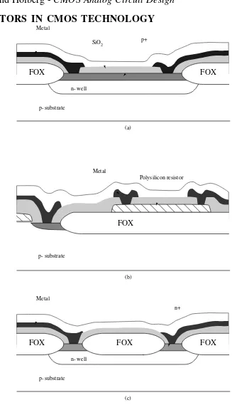
RESISTORS IN CMOS TECHNOLOGY
Figure 2.4-4 Resistors. (a) Diffused (b) Polysilicon (c) N-well p- substrate
FOX FOX
SiO2 Metal
(a) n- well
p+
p- substrate
FOX
(b)
Polysilicon resistor Metal
(c) p- substrate
FOX FOX
Metal
n- well
n+
PASSIVE COMPONENT SUMMARY (0.8µm Technology)
Component
Type Range of Values MatchingAccuracy TemperatureCoefficient CoefficientVoltage AccuracyAbsolute Poly/poly
capacitor 0.8-1.0 fF/µm2 0.05% 50 ppm/°C 50ppm/V ±10% MOS
capacitor 2.2-2.5 fF/µm2 0.05% 50 ppm/°C 50ppm/V ±10% MOM
capacitor 0.02-0.03 fF/µm2 1.5% ±10% Diffused
resistor 20-150 Ω/sq. 0.4% 1500 ppm/°C 200ppm/V ±35% Polysilicide R 2-15 Ω/sq.
Poly resistor 20-40 Ω/sq. 0.4% 1500 ppm/°C 100ppm/V ±30% N-well
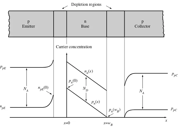
BIPOLARS IN CMOS TECHNOLOGY
Figure 2.5-1 Substrate BJT available from a bulk CMOS process. Collector (p- substrate)
FOX FOX
Metal
n- well
Base (n+)
FOX
Emitter (p+)
NA
NA ND
Figure 2.5-2 Minority carrier concentrations for a bipolar junction transistor.
ppE
npE
ppC
ppC nn(x)
pn(x) pn(0)
pn(wB) npE(0)
x=0 x=wB x
Carrier concentration Depletion regions
WB
p
II.6 - LATCHUP
Figure 2.5-3 (a) Parasitic lateral NPN and vertical PNP bipolar transistor in CMOS integrated circuits. (b) Equivalent circuit of the SCR formed from the parasitic bipolar transistors.
(b)
VDD
RP-
RN-B
A
Q1
Q2
G D=A
S
G D=B
S
p-substrate
FOX n+ n+ FOX FOX
p+ p+ p+ n+
n-well
RP- RN-Q1
Q2
(a)
VDD
PREVENTING LATCHUP
Figure 2.5-4 Preventing latch-up using guard bars in an n-well technology n-well
p- substrate FOX
n+ guard bars
n-channel transistor p+ guard bars
p-channel transistor
II.7 - ESD PROTECTION
Figure 2.5-5 Electrostatic discharge protection circuitry. (a) Electrical equivalent circuit (b) Implementation in CMOS technology
p-substrate
FOX
Metal
n-well
FOX
n+ p+
(a)
VDD
VSS
To internal gates
Bonding Pad
(b) p+ – n-well diode
n+ – substrate diode
II.8 - GEOMETRICAL CONSIDERATIONS
Design Rules for a Double-Metal, Double-Polysilicon, N-Well, Bulk CMOS Process.
Minimum Dimension Resolution (λ) 1. N-Well
1A. width ...6 1B. spacing ... 12 2. Active Area (AA)
2A. width ...4 Spacing to Well
2B. AA-n contained in n-Well...1 2C. AA-n external to n-Well... 10 2D. AA-p contained in n-Well...3 2E. AA-p external to n-Well...4 Spacing to other AA (inside or outside well)
2F. AA to AA (p or n)...3 3. Polysilicon Gate (Capacitor bottom plate)
3A. width...2 3B. spacing ...3 3C. spacing of polysilicon to AA (over field)...1 3D. extension of gate beyond AA (transistor width dir.) ...2 3E. spacing of gate to edge of AA (transistor length dir.) ...4 4. Polysilicon Capacitor top plate
5A. size ... 2x2 5B. spacing ...4 5C. spacing to polysilicon gate ...2 5D. spacing polysilicon contact to AA ...2 5E. metal overlap of contact ...1 5F. AA overlap of contact ...2 5G. polysilicon overlap of contact...2 5H. capacitor top plate overlap of contact...2 6. Metal-1
6A. width...3 6B. spacing ...3 7. Via
7A. size ... 3x3 7B. spacing ...4 7C. enclosure by Metal-1...1 7D. enclosure by Metal-2...1 8. Metal-2
8A. width...4 8B. spacing ...3 Bonding Pad
9. Passivation Opening (Pad)
1A 1B
3A
3B
3C 3E 3D
2A
2B
2C
2D
2E
2F
5F 5G 5H 5B
5D
5E 5A
5C
4C 4B
4A
8B 8A
9B
9A
9C
N-WELL N-AA P-AA
POLYSILICON GATE
CONTACT VIA METAL-1
METAL-2 POLYSILICON CAPACITOR
PASSIVATION 6B
6A 7C
7A
7D
7B
Transistor Layout
Figure 2.6-3 Example layout of an MOS transistor showing top view and side view at the cut line indicated.
Contact
Polysilicon gate
Active area drain/source
Metal 1 W
L
Cut
FOX FOX
Metal
SYMMETRIC VERSUS PHOTOLITHOGRAPHIC INVARIANT
Figure 2.6-4 Example layout of MOS transistors using (a) mirror symmetry, and
(b) photolithographic invariance.
(a) (b)
Resistor Layout
Figure 2.6-5 Example layout of (a) diffusion or polysilicon resistor and (b) Well resistor
along with their respective side views at the cut line indicated.
Metal 1 Active area or Polysilicon
Contact
(a) Diffusion or polysilicon resistor L
W
Metal 1 Well diffusion
Contact
(b) Well resistor L
W Active area
FOX FOX FOX
Metal
Active area (diffusion)
FOX FOX
Metal
Active area (diffusion)
Well diffusion
Cut Cut
Substrate
Capacitor Layout
Polysilicon gate FOX
Metal Polysilicon 2
Cut
Polysilicon gate Polysilicon 2
FOX
Metal 3 Metal 2 Metal 1
Metal 3 Metal 2 Metal 1 Metal 3
Metal 2
Metal 1 Via 2
Via 2
Via 1 Cut
(a)
(b)
Metal 1 Substrate
III. CMOS MODELS
Contents
III.1 Simple MOS large-signal model Strong inversion
Weak inversion III.2 Capacitance model
III.3 Small-signal MOS model III.4 SPICE Level-3 model
Perspective
DEVICES SYSTEMS
CIRCUITS
Chapter 2 CMOS Technology
Chapter 3 CMOS Device
Modeling
Chapter 4 Device Characterization Chapter 7
CMOS Comparators
Chapter 8 Simple CMOS OP
AMPS
Chapter 9 High Performance
OTA's
Chapter 5 CMOS Subcircuits
Chapter 6 CMOS Amplifiers Chapter 10
D/A and A/D Converters
Chapter 11 Analog Systems
III.1 - MODELING OF CMOS ANALOG CIRCUITS
Objective
1. Hand calculations and design of analog CMOS circuits. 2. Efficiently and accurately simulate analog CMOS circuits.
Large Signal Model
The large signal model is nonlinear and is used to solve for the dc values of the device currents given the device voltages.
The large signal models for SPICE: Basic drain current models
-1. Level 1 - Shichman-Hodges (VT, K', γ, λ, φ, and NSUB)
2. Level 2 - Geometry-based analytical model. Takes into account second-order effects (varying channel charge, short-channel, weak inversion, varying surface mobility, etc.)
3. Level 3 - Semi-empirical short-channel model
4. Level 4 - BSIM model. Based on automatically generated parameters from a process characterization. Good weak-strong inversion transition.
Basic model auxilliary parameters include capacitance [Meyer and
Ward-Dutton (charge-conservative)], bulk resistances, depletion regions, etc..
Small Signal Model
Based on the linearization of any of the above large signal models.
Simulator Software
SPICE2 - Generic SPICE available from UC Berkeley (FORTRAN) SPICE3 - Generic SPICE available from UC Berkeley (C)
Transconductance Characteristics of NMOS when VDS = 0.1V
vGS ≤ VT:
vGS iD
VT 2VT 3VT
0 0
vGS
= VT
+ -=0.1VVDS +
-p substrate (bulk)
Gate Drain
iD
Source and bulk
vGS = 2VT:
vGS iD
VT 2VT 3VT
0 0 VDS =0.1V + -+ -vGS
= 2VT
p substrate (bulk)
Gate Drain
iD
Source and bulk
vGS = 3VT:
vGS iD
VT 2VT 3VT
0 0
vGS
= 3VT
+ -=0.1VVDS +
-p substrate (bulk)
Gate Drain
iD
Output Characteristics of NMOS for VGS = 2VT
vDS = 0V:
vDS
= 0V
p substrate (bulk)
Gate Drain + -iD + -Source and bulk VGS
= 2VT
iD
vDS
0
0 0.5VT VT
vDS = 0.5VT:
p substrate (bulk)
Gate Drain + -iD + -Source and bulk
vDS =
0.5VT
VGS
= 2VT
iD
vDS
0
0 0.5VT VT
vDS = VT:
iD
vDS 0 0.5VT VT
p substrate (bulk)
Gate Drain + -iD + -Source and bulk vDS =VT x VGS
Output Characteristics of NMOS when vDS= 4VT
vGS = VT:
iD
VT vDS
0
0 2VT 3VT 4VT
vDS(sat) p substrate (bulk)
Gate Drain + -iD + -Source and bulk
vDS =
4VT vGS =
VT
vGS = 2VT:
iD
VT vDS
0
0 2VT 3VT 4VT
vDS(sat) p substrate (bulk)
Gate Drain + -iD + -Source and bulk
vGS =
2VT
vDS =
4VT
vGS = 3VT:
iD
VT vDS
0
0 2VT 3VT 4VT
vDS(sat)
vDS =
4VT
p substrate (bulk)
Gate Drain + -iD + -Source and bulk
vGS=
Output Characteristics of an n-channel MOSFET
Transconductance Characteristics of an n-channel MOSFET
vDS (V)
0 2 4 6 8 10
0 iD (mA)
VGS=1V
VGS=2V
VGS=3V
VGS=4V
VGS=5V
0.5 1.0 1.5
2.0 Output Characteristics of a n-channel MOSFET
.MODEL MN1K100 NMOS VTO=1 KP=200U LAMBDA=0.01 .DC VDS 0 10 0.5 VGS 1 5 1
MOSFET1 2 1 0 0 MN1K100 .PRINT DC ID(MOSFET1) VGS 1 0
VDS 2 0 .PROBE .END
0 iD (mA)
0 1
vGS(V)
VDS=8V
VDS=6V
VDS=2V
2 3 4 5
0.5 1.0 1.5 2.0
VDS=4V Transconductance Characteristics of a n-channel MOSFET
.MODEL MN1K100 NMOS VTO=1 KP=200U LAMBDA=0.01 .DC VGS 0 5 0.5 VDS 2 8 2
MOSFET1 2 1 0 0 MN1K100 .PRINT DC ID(MOSFET1) VGS 1 0
SIMPLIFIED SAH MODEL DERIVATION
Model-n+ n+
y v(y)
dy
0 y y+dy L p-Source Drain
+ -vGS -iD + vDS
• Let the charge per unit area in the channel inversion layer be QI(y) = Cox[vGS − v(y) − VT] (coulombs/cm2) • Define sheet conductivity of the inversion layer per square as
σS = µoQI(y) cmv·s 2 coulombs cm2 = ampsvolt = Ω/sq. 1 • Ohm's Law for current in a sheet is
JS = iW = D σSEy = σS dvdy . Rewriting Ohm's Law gives,
dv = σiD
SW dy =
iDdy µoQI(y)W
where dv is the voltage drop along the channel in the direction of y. Rewriting as
iD dy = WµoQI(y)dv
and integrating along the channel for 0 to L gives
⌡ ⌠
0 L
iDdy = ⌡⌠
0 vDS
WµoQI(y)dv = ⌡⌠ 0 vDS
WµoCox[vGS−v(y)−VT] dv After integrating and evaluating the limits
iD = WµLoCox
ILLUSTRATION OF THE SAH EQUATION
Plotting the Sah equation as iD vs. vDS results in -iD
vDS = vGS - VT
Increasing values of vGS
Saturation Region Non-Sat Region
vDS
Define vDS(sat) = vGS − VT
Regions of Operation of the MOS Transistor 1.) Cutoff Region:
iD = 0, vGS − VT < 0
(Ignores subthreshold currents) 2.) Non-saturation Region
iD = µC2L oxW2(vGS − VT) − vDS vDS , 0 < vDS < vGS − VT
3.) Saturation Region
SAH MODEL ADJUSTMENT TO INCLUDE EFFECTS OF V DS ON V T From the previous derivation:
⌡ ⌠
0 L
iD dy = ⌡⌠
0 vDS
WµoQI(y)dy = ⌡⌠ 0 vDS
WµoCox[vGS − v(y) − VT]dv
Assume that the threshld voltage varies across the channel in the following way:
VT(y) = VT + ∆v(y)
where VT is the value of the threshold voltage at the source end of the channel.
Integrating the above gives,
iD = WµLoCox
(vGS−VT)v(y) − (1+∆) v22(y) vDS
0 or
iD = WµLoCox
(vGS−VT)vDS − (1+∆) v2DS2
To find vDS(sat), set the derivative of iD with respect to vDS equal to zero and solve for vDS = vDS(sat) to get,
vDS(sat) = vGS1 + ∆ − VT
Therefore, in the saturation region, the drain current is
EFFECTS OF BACK GATE (BULK-SOURCE)
Bulk-Source (vBS) influence on the transconductance
characteristics-vGS
iD Decreasing values
of bulk-source voltage
VT0 VT1 VT2 VT3
VBS = 0
vDS≥ vGS - VT
In general, the simple model incorporates the bulk effect into VT by the following empirically developed
EFFECTS OF THE BACK GATE - CONTINUED
Illustration-VSB0 = 0V:
Poly
p+ n+ n+
p
-+
-Bulk Source
Gate Drain VDS>0
VGS>VT
Substrate/Bulk VSB0=0V
VSB1>0V:
Poly
p+ n+ n+
p
-+
-Bulk Source
Gate Drain VDS>0
VGS>VT
Substrate/Bulk VSB1
VSB2 > VSB1:
Poly
p+ n+ n+
p
-+
-Bulk Source
Gate Drain VDS>0
VGS>VT
SAH MODEL INCLUDING CHANNEL LENGTH MODULATION N-channel reference convention:
+ + -+
-vBS
vDS
vGS
iD
D
B
S G
Non-saturation-iD = WµLoCox
(vGS − VT)vDS − vDS22
Saturation-iD = WµLoCox
(vGS − VT)vDS(sat) − vDS(sat) 2
2 (1 + λvDS)
= Wµ2LoCox (vGS − VT) 2 (1 + λvDS)
where:
µo = zero field mobility (cm2/volt·sec)
Cox = gate oxide capacitance per unit area (F/cm2) λ= channel-length modulation parameter (volts-1) VT = VT0 + γ 2|φf| + |vBS| − 2|φf|
VT0 = zero bias threshold voltage γ = bulk threshold parameter (volts1/2)
2|φf| = strong inversion surface potential (volts)
OUTPUT CHARACTERISTICS OF THE MOS TRANSISTOR
-VT
vGS
vDS - VT
iD /ID0
0.75 1.0
0.5 0.25 0
0 0.5 1.0 1.5 2.0 2.5
vGS-VT
- VT = 0
vGS-VT
VGS0 - VT = 0.5
vGS-VT
- VT = 0.707
vGS-VT
VGS0 - VT = 0.867
VGS0 - VT = 1.0
Channel modulation effects
vDS
VGS0 - VT
Non-Sat
Region Saturation Region
Cutoff Region VGS0
VGS0
= vGS
Notation:
ß = K'
W
L = (µoCox) WL
Note:
GRAPHICAL INTERPRETATION OF λ
Assume the MOS is transistor is
saturated-∴ iD =µC2L (voxW GS − VT) 2(1 + λvDS) Define iD(0) = iD when vDS = 0V.
∴ iD(0) = µC2L (voxW GS − VT)2 Now,
iD = iD(0) [1+λvDS] = iD(0) + λiD(0) vDS or
vDS =
1
λiD (0) iD − 1λ Matching with y = mx + b gives
vDS
iD
iD(0)
1
λiD(0)
1
-1
λ
or
vDS
iD
-1
λ
iD1(0)
iD2(0)
iD3(0 VGS3
VGS2
VGS1
SPICE LEVEL 1 MODEL PARAMETERS FOR A TYPICAL BULK CMOS PROCESS (0.8µm)
Model Parameter
Parameter Description
Typical Parameter Value
NMOS PMOS
Units
VT0 ThresholdVoltage forVBS = 0V 0.75±0.15 −0.85±0.15 Volts K' Transconductance Parameter
(sat.)
110±10% 50±10% µA/V2
γ Bulk Threshold Parameter 0.4 0.57 V
λ Channel Length Modulation Parameter
0.04 (L=1 µm) 0.01 (L=2 µm)
0.05 (L = 1 µm)
0.01 (L = 2 µm) V-1
φ = 2φF Surface potential at strong
inversion
0.7 0.8 Volts
WEAK INVERSION MODEL (Simple)
0 vGS
iD
VON
VT 0 vGS
iD (nA)
VON VT
Weak inversion
region Strong inversion
region
1.0 10.0 100.0 1000.0
This model is appropriate for hand calculations but it does not accommodate a smooth transition into the strong-inversion region.
iD ≅ WL IDO exp qvnkTGS
The transition point where this relationship is valid occurs at approximately
vgs < VT + n kTq
Weak-Moderate-Strong Inversion Approximation
0 vGS
iD (nA)
Weak inversion
region Strong inversion
region
1.0 10.0 100.0 1000.0
INTRINSIC CAPACITORS OF THE MOSFET
Types of MOS Capacitors
1. Depletion capacitance (CBD and CBS) 2. Gate capacitances (CGS, CGD, and CGB)
Figure 3.2-4 Large-signal, charge-storage capacitors of the MOS device.
SiO2
Bulk
Source Drain
Gate
CBS CBD
C4
C1 C2
Depletion Capacitors Bulkdrain pn junction
-CBD
CBD0
VBD
φB
Reverse Bias ForwardBias (FC).φB
Capacitance approximation for strong for-ward bias
xArea
CBD =
CBD0 ABD
1 − vφBD
B
MJ andCBS =
CBS0 ABS
1 − vφBS
B MJ
where,
ABD (ABS) = area of the bulk-drain (bulk-source)
φΒ = bulk junction potential (barrier potential)
MJ = bulk junction grading coefficient ( 0.33 ≤ MJ ≤ 0.5)
For strong forward bias, approximate the behavior by the tangent to the above CBD or CBS curve at vBD or vBS equal to (FC)·φB.
CBD =
CBD0ABD
(1+FC)1+MJ
1 − (1+MJ)FC + FC
vBD
φB , vBD > (FC)·φ B and
CBD =
CBS0ABS
(1+FC)1+MJ
1 − (1+MJ)FC + FC
vBS
Bottom & Sidewall Approximations
SiO2 Polysilicon gate Bulk A B C D E F G H
Drain bottom = ABCD
Drain sidewall = ABFE + BCGF + DCGH + ADHE
Source Drain
CBX = (CJ)(AX)
1 −
vBX PB
MJ +
(CJSW)(PX)
1 −
vBX PB
MJSW , vBX ≤ (FC)(PB)
and
CBX = (1 − (CJ)(AX) FC)1+MJ
1 − (1 + MJ)FC + MJ vBX PB
+ (CJSW)(PX) (1 − FC)1+MJSW
1 − (1 + MJSW)FC + vBX
PB (MJSW) , vBX ≥ (FC)(PB)
where
Overlap Capacitance
Bulk
LD
Mask
W
Oxide encroachment
Actual
L (Leff)
Gate Mask L
Source-gate overlap capacitance CGS (C1)
Drain-gate overlap capacitance CGD (C3)
Source Drain
Gate
FOX FOX
Actual
W (Weff)
Gate to Bulk Overlap Capacitance
Bulk
Overlap Overlap
Source/Drain Gate
FOX C5 C5FOX
On a per-transistor basis, this is generally quite small
Channel Capacitance
C2 = Weff(L − 2LD)Cox = Weff(Leff)Cox
MOSFET Gate Capacitance Summary:
0 v
GS
Figure 3.2-7 Voltage dependence of C , C , and C as a function of V CGS
CGS, CGD
CGD CGB CGS, CGD
C2 + 2C5
C1 +23_C 2
C1 +12_C 2
C1,C3
2C5
VT vDS +VT
Off Saturation
Non-Saturation
vDS = constant vBS = 0
Capacitance
vDS - VT
iD
0
0 0.5 1.0 1.5 2.0 2.5
Non-Sat Region
Saturation Region
Cutoff Region = vGS
CGS, CGD, and CGB
Off
CGB = C2 + 2C5 = Cox(Weff)(Leff) + CGBO(Leff) CGS = C1 ≅ Cox(LD)(Weff) = CGSO(Weff)
CGD = C3 ≅ Cox(LD)(Weff) = CGDO(Weff) Saturation
CGB = 2C5 = CGBO (Leff)
CGS = C1 + (2/3)C2 = Cox(LD + 0.67Leff)(Weff)
= CGSO(Weff) + 0.67Cox(Weff)(Leff)
CGD = C3 ≅ Cox(LD)(Weff) = CGDO(Weff) Nonsaturated
CGB = 2C5 = CGBO (Leff)
CGS = C1 + 0.5C2 = Cox(LD + 0.5Leff)(Weff)
= (CGSO + 0.5CoxLeff)Weff
CGD = C3 + 0.5C2 = Cox(LD + 0.5Leff)(Weff)
Small-Signal Model for the MOS Transistor
B D
S
G i
nD
Cbd
Cgd
Cgs
Cgb gmvgs
rD
rS
Cbs
Figure 3.3-1 Small-signal model of the MOS transistor. gmbsvbs
gds
gbs gbd inrD
inrS
gbd= ∂IBD
∂VBD (at the quiescent point) ≅ 0 and
gbs= ∂ IBS
∂VBS (at the quiescent point) ≅ 0
The channel conductances, gm, gmbs, and gds are defined as gm= ∂
ID
∂VGS (at the quiescent point)
gmbs= ∂ID
∂VBS (at the quiescent point)
and
gds= ∂ID
Saturation Region
gm= (2K'W/L)| ID|(1 +λ VDS) ≅ (2K'W/L)|ID|
gmbs=−∂ID
∂VSB=−
∂ID
∂VT
∂VT
∂VSB
Noting that ∂ID
∂VT=
−∂ID
∂VGS , we get
gmbs=gm γ
2(2|φF|+VSB)1/2
=η gm
gds=go=
IDλ
1 +λ VDS≅ID λ
Relationships of the Small Signal Model Parameters upon the DC Values of Voltage and Current in the Saturation Region.
Small Signal
Model Parameters DC Current DC Current andVoltage DC Voltage
gm ≅ (2K' IDW/L)1/2 _ ≅ 2K' W
L (VGS -VT)
gmbs γ (2IDβ)1/2
2(2|φF | +VSB) 1/2
γ( β(VGS −VT) )
2(2|φF | + VSB)1/2
N
onsaturation region
gm= ∂Id ∂VGS
=β VDS
gmbs= ∂ID
∂VBS
= βγVDS
2(2|φF |+ VSB)1/2
and
gds=β(VGS−VT −VDS)
Relationships of the Small-Signal Model Parameters upon the DC Values of Voltage and Current in the Nonsaturation Region.
Small Signal
Model Parameters DC Voltage and/or CurrentDependence
gm = β VDS
gmbs βγ VDS
2(2|φF | +VSB)1/2
gds = β (VGS−VT −VDS)
Noise
i 2nrD= 4kT
rD ∆f (A
2)
i 2nrS= 4kT
rS ∆f (A
2)
and
i 2nD=
8kTgm(1+η)
3 +
(KF )ID
f CoxL2 ∆f (A
SPICE Level 3 Model
The large-signal model of the MOS device previously discussed neglects many important second-order effects. Most of these second-order effects are due to narrow or short channel dimensions (less than about 3µm). We shall also consider the effects of temperature upon the parameters of the MOS large signal model.
We first consider second-order effects due to small geometries. When vGS is greater than VT, the drain current for a small device can be given as
Drain Current
iDS = BETA
vGS−VT−
1 +fb
2 vDE ⋅vDE (1)
BETA = KP WLeff
eff = µeffCOX
Weff
Leff (2)
Leff=L− 2(LD) (3)
Weff=W− 2(WD) (4)
vDE = min(vDS , vDS (sat)) (5)
fb = fn+ GAMMA ⋅ fs
4(PHI +vSB)1/2 (6)
Note that PHI is the SPICE model term for the quantity 2φf . Also be aware that PHI is
always positive in SPICE regardless of the transistor type (p- or n-channel).
fn =DELTA Weff
πεsi
2 ⋅ COX (7)
fs = 1 − xj Leff
LD +wc xj
1 − wp xj+wp
2 1/2
−LD
xj (8)
wp = xd (PHI + vSB)1/2 (9)
xd =
2⋅εsi q ⋅ NSUB
1/2
wc = xj k1 + k2
wp
xj − k3 wp xj 2 (11)
k1 = 0.0631353 , k2 = 0.08013292 , k3 = 0.01110777
Threshold V oltage
VT = Vbi−
ETA⋅8.15-22
Cox Leff3
vDS+ GAMMA ⋅fs( PHI +vSB)1/2+fn( PHI +vSB) (12)
vbi = vfb+ PHI (13)
or
vbi = VTO − GAMMA ⋅ PHI (14)
Saturation Voltage
vsat = vgs−VT
1 +fb (15)
vDS(sat) = vsat + vC− v2sat+v2C
1/2
(16)
vC =
VMAX ⋅Leff
µs (17)
If VMAX is not given, then vDS(sat) = vsat
Effective Mobility
µs = U0
1 + THETA (vGS− VT) when VMAX = 0 (18)
µeff = µs 1 +vDE
vC
when VMAX > 0; otherwise µeff = µs (19)
Channel-Length Modulation
∆L = xdKAPPA (vDS−vDS(sat))1/2 (20)
when VMAX > 0
∆L = −ep⋅ xd 2 2+ep⋅ xd 2 2
2
+ KAPPA ⋅xd 2 ⋅ (vDS−vDS(sat))
1/2
(21)
where
ep =
vC (vC+ vDS(sat))
Leff vDS (sat) (22)
iDS = iDS
1 − ∆L (21)
Weak Inversion Model (Level 3)
In the SPICE Level 3 model, the transition point from the region of strong inversion to the weak inversion characteristic of the MOS device is designated as von and is greater
than VT.von is given by
von = VT + fast (1)
where
fast = kT q
1 + qCOX⋅ NFS + GAMMA ⋅ fs (PHI + vSB)
1/2 + f
n (PHI + vSB)
2(PHI + vSB) (2)
N F S is a parameter used in the evaluation of vo n and can be extracted from
measurements. The drain current in the weak inversion region, vGS less than von , is given
as
iDS = iDS (von , vDE , vSB) e
vGS - von
fast (3)
where iDS is given as (from Eq. (1), Sec. 3.4 with vGS replaced with von) iDS = BETAvon−VT −
1 +fb
Typical Model Parameters Suitable for SPICE Simulations Using Level-3 Model (Extended Model). These Values Are Based upon a 0.8µm Si-Gate Bulk CMOS n-Well Process
Parameter Parameter Typical Parameter Value
Symbol Description N-Channel P-Channel Units VTO Threshold 0.7 ± 0.15 −0.7 ± 0.15 V
UO mobility 660 210 cm2/V-s
DELTA Narrow-width threshold
adjust factor 2.4 1.25
ETA Static-feedback threshold
adjust factor 0.1 0.1
KAPPA Saturation field factor in
channel-length modulation 0.15 2.5 1/V THETA Mobility degradation factor 0.1 0.1 1/V NSUB Substrate doping 3×10¹⁶ 6×1016 cm-3
TOX Oxide thickness 140 140 Å
XJ Mettallurgical junction
depth 0.2 0.2 µm
WD Delta width µm
LD Lateral diffusion 0.016 0.015 µm NFS Parameter for weak
inversion modeling 7×10¹¹ 6×1011 cm
-2
CGSO 220 × 10−12 220 × 10−12 F/m CGDO 220 × 10−12 220 × 10−12 F/m CGBO 700 × 10−12 700 × 10−12 F/m CJ 770 × 10−6 560 × 10−6 F/m2
CJSW 380 × 10−12 350 × 10−12 F/m
MJ 0.5 0.5
MJSW 0.38 0.35
NFS Parameter for weak
inversion modeling 7×10¹¹ 6×1011 cm
Temperature Dependence
The temperature-dependent variables in the models developed so far include the: Fermi potential, PHI, EG,bulk junction potential of the source-bulk and drain-bulk junctions, PB, the reverse currents of the pn junctions, IS, and the dependence of mobility upon
temperature. The temperature dependence of most of these variables is found in the equations given previously or from well-known expressions. The dependence of mobility upon temperature is given as
UO(T) = UO(T0) T T0 BEX
where BEX is the temperature exponent for mobility and is typically -1.5.
vtherm(T) =KT
q
EG(T) = 1.16 − 7.02 ⋅ 10−4⋅ T2 T+ 1108.0
PHI(T) = PHI(T0) ⋅ TT
0 −vtherm(T)
3 ⋅ lnT
T0 +
EG(T0) vtherm(T0) −
EG(T) vtherm(T) vbi (T) = vbi (T0) +PHI(T) −2 PHI(T0)+EG(T0) 2− EG(T)
VT0(T) =vbi (T) + GAMMA PHI(T)
PHI(T)= 2 ⋅ vtherm ln NSUB
ni (T)
ni(T) = 1.45 ⋅ 1016⋅
T T0
3/2
⋅ exp
EG ⋅T T0− 1 ⋅
1 2 ⋅vtherm(T0)
For drain and source junction diodes, the following relationships apply.
PB(T) = PB ⋅ T
T0 −vtherm(T)
3 ⋅ lnT
T0 +
EG(T0)
vtherm(T0) −
EG(T) vtherm(T) IS(T) = IS(T0)
N ⋅ exp
EG(T0)
vtherm(T0) −
EG(T)
vtherm(T)+ 3 ⋅ ln
T T0
SPICE Simulation of MOS Circuits
Minimum required terms for a transistor instance follows: M1 3 6 7 0 NCH W=100U L=1U
“M,” tells SPICE that the instance is an MOS transistor (just like “R” tells SPICE that an instance is a resistor). The “1” makes this instance unique (different from M2, M99, etc.)
The four numbers following”M1” specify the nets (or nodes) to which the drain, gate, source, and substrate (bulk) are connected. These nets have a specific order as indicated below:
M<number> <DRAIN> <GATE> <SOURCE> <BULK> ...
Following the net numbers, is the model name governing the character of the particular instance. In the example given above, the model name is “NCH.” There must be a model description of “NCH.”
The transistor width and length are specified for the instance by the “W=100U” and “L=1U” expressions.
The default units for width and length are meters so the “U” following the number 100 is a multiplier of 10-6. [Recall that the following multipliers can be used in SPICE: M, U, N, P, F, for 10-3, 10-6, 10-9, 10-12 , 10-15 , respectively.]
Additional information can be specified for each instance. Some of these are Drain area and periphery (AD and PD) ← calc depl cap and leakage Source area and periphery (AS and PS) ← calc depl cap and leakage Drain and source resistance in squares (NRD and NRS)
Multiplier designating how many devices are in parallel (M) Initial conditions (for initial transient analysis)
Geometric Multiplier: M
To apply the “unit-matching” principle, use the geometric multiplier feature rather than scale W/L.
This:
M1 3 2 1 0 NCH W=20U L=1U
is not the same as this:
M1 3 2 1 0 NCH W=10U L=1U M=2
The following dual instantiation is equivalent to using a multiplier
M1A 3 2 1 0 NCH W=10U L=1U M1B 3 2 1 0 NCH W=10U L=1U
(a)M1 3 2 1 0 NCH W=20U L=1U. (b) M1 3 2 1 0 NCH W=10U L=1U M=1. .
MODEL Description
A SPICE simulation file for an MOS circuit is incomplete without a
description of the model to be used to characterize the MOS transistors used in the circuit. A model is described by placing a line in the simulation file using the following format.
.MODEL <MODEL NAME> <MODEL TYPE> <MODEL PARAMETERS>
MODEL NAME e.g., “NCH”
MODEL TYPE either “PMOS” or “NMOS.”
MODEL PARAMETERS :
LEVEL=1 VTO=1 KP=50U GAMMA=0.5LAMBDA=0.01
SPICE can calculate what you do not specify You must specify the following
• surface state density, NSS, in cm-2 • oxide thickness, TOX, in meters • surface mobility, UO, in cm2/V-s, • substrate doping, NSUB, in cm-3
The equations used to calculate the electrical parameters are
VTO =φMS−
q(NSS)
(εox/TOX)
+(2q⋅εsi⋅ NSUB ⋅ PHI)1/2
(εox/TOX)
+ PHI
KP = UO TOXεox
GAMMA =(2q⋅εsi⋅ NSUB)1/2
(εox/TOX)
and
PHI = 2φF=
2kT q ln
NSUB
ni
Other parameters:
IS: Reverse current of the drain-bulk or source-bulk junctions in Amps JS: Reverse-current density in A/m2
JS requires the specification of AS and AD on the model line. If IS is specified, it overrides JS. The default value of IS is usually 10-14 A. RD: Drain ohmic resistance in ohms
RS: Source ohmic resistance in ohms
RSH: Sheet resistance in ohms/square. RSH is overridden if RD or RS are entered. To use RSH, the values of NRD and NRS must be entered on the model line.
The drain-bulk and source-bulk depletion capacitors CJ: Bulk bottom plate junction capacitance MJ: Bottom plate junction grading coefficient CJSW: Bulk sidewall junction capacitance MJSW: Sidewall junction grading coefficient
If CJ is entered as a model parameter it overrides the calculation of CJ using NSUB, otherwise, CJ is calculated using NSUB.
If CBD and CBS are entered, these values override CJ and NSUB calculations. In order for CJ to result in an actual circuit capacitance, the transistor instance must include AD and AS.
In order for CJSW to result in an actual circuit capacitance, the transistor instance must include PD and PS.
CGSO: Gate-Source overlap capacitance (at zero bias) CGDO: Gate-Drain overlap capacitance (at zero bias) AF: Flicker noise exponent
KF: Flicker noise coefficient
TPG: Indicates type of gate material relative to the substrate TPG=1 > gate material is opposite of the substrate TPG=-1 > gate material is the same as the substrate TPG=0 > gate material is aluminum
1
IV. CMOS PROCESS CHARACTERIZATION
Contents
IV.1 Measurement of basic MOS level 1 parameters IV.2 Characterization of the extended MOS model IV.3 Characterization other active components IV.4 Characterization of resistance
IV.5 Characterization of capacitance
Organization
DEVICES SYSTEMS
CIRCUITS
Chapter 2 CMOS Technology
Chapter 3 CMOS Device
Modeling
Chapter 4 Device Characterization Chapter 7
CMOS Comparators
Chapter 8 Simple CMOS
Opamps
Chapter 9 High Performance
Opamps
Chapter 5 CMOS Subcircuits
Chapter 6 CMOS Amplifiers Chapter 10
D/A and A/D Converters
Chapter 11 Analog Systems
1
I. Characterization of the Simple Transistor Model
Determine VT0(VSB = 0), K', γ, and λ.
Terminology:
K'S for the saturation region K'L for the nonsaturation region
iD = K'S
Weff
2Leff (vGS - VT)2 (1 + λ vDS ) (1)
iD = K'L
Weff Leff
(vG S - V T) vD S - v2DS