DATA SHEET
Product specification
Supersedes data of 1998 Jun 04
2003 Jun 25
INTEGRATED CIRCUITS
74HC595; 74HCT595
2003 Jun 25 2
Philips Semiconductors Product specification
8-bit serial-in, serial or parallel-out shift
register with output latches; 3-state
74HC595; 74HCT595
FEATURES • 8-bit serial input
• 8-bit serial or parallel output
• Storage register with 3-state outputs
• Shift register with direct clear
• 100 MHz (typical) shift out frequency
• ESD protection:
HBM EIA/JESD22-A114-A exceeds 2000 V MM EIA/JESD22-A115-A exceeds 200 V.
APPLICATIONS
• Serial-to-parallel data conversion
• Remote control holding register.
DESCRIPTION
The 74HC/HCT595 are high-speed Si-gate CMOS devices and are pin compatible with low power Schottky TTL (LSTTL). They are specified in compliance with JEDEC standard no. 7A.
The 74HC/HCT595 is an 8-stage serial shift register with a storage register and 3-state outputs. The shift register and storage register have separate clocks.
Data is shifted on the positive-going transitions of the SH_CP input. The data in each register is transferred to the storage register on a positive-going transition of the ST_CP input. If both clocks are connected together, the shift register will always be one clock pulse ahead of the storage register.
The shift register has a serial input (DS) and a serial standard output (Q7’) for cascading. It is also provided with asynchronous reset (active LOW) for all 8 shift register stages. The storage register has 8 parallel 3-state bus driver outputs. Data in the storage register appears at the output whenever the output enable input (OE) is LOW.
QUICK REFERENCE DATA
GND = 0 V; Tamb= 25°C; tr= tf= 6 ns.
Notes
1. CPD is used to determine the dynamic power dissipation (PDinµW).
PD= CPD×VCC2×fi×N +Σ(CL×VCC2×fo) where:
fi= input frequency in MHz;
fo= output frequency in MHz;
CL= output load capacitance in pF;
VCC= supply voltage in Volts;
N = total load switching outputs;
Σ(CL×VCC2×fo) = sum of the outputs.
2. For 74HC595 the condition is VI= GND to VCC.
For 74HCT595 the condition is VI= GND to VCC−1.5 V.
SYMBOL PARAMETER CONDITIONS TYPICAL UNIT
74HC 74HCT
tPHL/tPLH propagation delay CL= 50 pF; VCC= 4.5 V
SH_CP to Q7’ 19 25 ns
SH_CP to Qn 20 24 ns
MR to Q7’ 100 52 ns
fmax maximum clock frequency SH_CP and ST_CP 100 57 MHz
CI input capacitance 3.5 3.5 pF
2003 Jun 25 3
Philips Semiconductors Product specification
8-bit serial-in, serial or parallel-out shift
register with output latches; 3-state
74HC595; 74HCT595
FUNCTION TABLE
See note 1.
Note
1. H = HIGH voltage level; L = LOW voltage level;
↑= LOW-to-HIGH transition;
↓= HIGH-to-LOW transition; Z = high-impedance OFF-state; n.c. = no change;
X = don’t care.
ORDERING INFORMATION
INPUT OUTPUT
FUNCTION
SH_CP ST_CP OE MR DS Q7’ Qn
X X L L X L n.c. a LOW level on MR only affects the shift registers X ↑ L L X L L empty shift register loaded into storage register X X H L X L Z shift register clear; parallel outputs in high-impedance
OFF-state
↑ X L H H Q6’ n.c. logic high level shifted into shift register stage 0; contents of all shift register stages shifted through, e.g. previous state of stage 6 (internal Q6’) appears on the serial output (Q7’)
X ↑ L H X n.c. Qn’ contents of shift register stages (internal Qn’) are transferred to the storage register and parallel output stages
↑ ↑ L H X Q6’ Qn’ contents of shift register shifted through; previous contents of the shift register is transferred to the storage register and the parallel output stages
TYPE NUMBER
PACKAGE TEMPERATURE
RANGE PINS PACKAGE MATERIAL CODE
74HC595N −40 to +125°C 16 DIP16 plastic SOT38-4
74HCT595N −40 to +125°C 16 DIP16 plastic SOT38-4
74HC595D −40 to +125°C 16 SO16 plastic SOT109-1
74HCT595D −40 to +125°C 16 SO16 plastic SOT109-1
74HC595DB −40 to +125°C 16 SSOP16 plastic SOT338-1
74HCT595DB −40 to +125°C 16 SSOP16 plastic SOT338-1
74HC595PW −40 to +125°C 16 TSSOP16 plastic SOT403-1
74HCT595PW −40 to +125°C 16 TSSOP16 plastic SOT403-1
74HC595BQ −40 to +125°C 16 DHVQFN16 plastic SOT763-1
2003 Jun 25 4
Philips Semiconductors Product specification
8-bit serial-in, serial or parallel-out shift
register with output latches; 3-state
74HC595; 74HCT595
PINNING
PIN SYMBOL DESCRIPTION
1 Q1 parallel data output 2 Q2 parallel data output 3 Q3 parallel data output 4 Q4 parallel data output 5 Q5 parallel data output 6 Q6 parallel data output 7 Q7 parallel data output
8 GND ground (0 V)
9 Q7’ serial data output
10 MR master reset (active LOW) 11 SH_CP shift register clock input 12 ST_CP storage register clock input 13 OE output enable (active LOW) 14 DS serial data input
15 Q0 parallel data output 16 VCC positive supply voltage
handbook, halfpage
Fig.1 Pin configuration DIP16, SO16 and (T)SSOP16.
Top view MBL893
Q7
Fig.2 Pin configuration DHVQFN16.
2003 Jun 25 5
Philips Semiconductors Product specification
8-bit serial-in, serial or parallel-out shift
register with output latches; 3-state
74HC595; 74HCT595
handbook, halfpage
Fig.3 Logic symbol.
handbook, halfpage
Fig.4 IEC logic symbol.
handbook, full pagewidth
ST_CP DS
SH_CP
MR
Q7' 8-STAGE SHIFT REGISTER
8-BIT STORAGE REGISTER 14
2003 Jun 25 6
Philips Semiconductors Product specification
8-bit serial-in, serial or parallel-out shift
register with output latches; 3-state
74HC595; 74HCT595
handbook, full pagewidth
STAGE 0 STAGES 1 to 6 STAGE 7
FF0 D
CP Q
R
LATCH D
CP Q
FF7 D
CP Q
R
LATCH D
CP Q
MLA010
D Q
Q1 Q2 Q3 Q4 Q5 Q6 Q7
Q7'
Q0 DS
ST_CP SH_CP
OE MR
2003 Jun 25 7
Philips Semiconductors Product specification
8-bit serial-in, serial or parallel-out shift
register with output latches; 3-state
74HC595; 74HCT595
handbook, full pagewidth
high-impedance OFF-state ST_CP
DS SH_CP
MR
OE
Q1 Q0
Q7' Q6
Q7
MLA005-1
2003 Jun 25 8
Philips Semiconductors Product specification
8-bit serial-in, serial or parallel-out shift
register with output latches; 3-state
74HC595; 74HCT595
RECOMMENDED OPERATING CONDITIONS
LIMITED VALUES
In accordance with the Absolute Maximum Rating System (IEC 60134); voltages are referenced to GND (ground = 0 V).
Note
1. For DIP16 packages: above 70°C derate linearly with 12 mW/K. For SO16 packages: above 70°C derate linearly with 8 mW/K. For SSOP16 packages: above 60°C derate linearly with 5.5 mW/K. For TSSOP16 packages: above 60°C derate linearly with 5.5 mW/K. For DHVQFN16 packages: above 60°C derate linearly with 4.5 mW/K.
SYMBOL PARAMETER CONDITIONS 74HC 74HCT UNIT
MIN. TYP. MAX. MIN. TYP. MAX.
VCC supply voltage 2.0 5.0 6.0 4.5 5.0 5.5 V
VI input voltage 0 − VCC 0 − VCC V
VO output voltage 0 − VCC 0 − VCC V
Tamb ambient temperature −40 − +125 −40 − +125 °C
tr, tf input rise and fall time VCC= 2.0 V − − 1000 − − − ns
VCC= 4.5 V − 6.0 500 − 6.0 500 ns
VCC= 6.0 V − − 400 − − − ns
SYMBOL PARAMETER CONDITIONS MIN. MAX. UNIT
VCC supply voltage −0.5 +7.0 V
IIK input diode current VI<−0.5 V to VI> VCC+ 0.5 V − ±20 mA
IOK output diode current VO<−0.5 V to VO> VCC+ 0.5 V − ±20 mA
IO output source or sink current VO=−0.5 V to VCC+ 0.5 V
Q7’ standard output − ±25 mA
Qn bus driver outputs − ±35 mA
ICC, IGND VCC or GND current − ±70 mA
Tstg storage temperature −65 +150 °C
2003 Jun 25 9
Philips Semiconductors Product specification
8-bit serial-in, serial or parallel-out shift
register with output latches; 3-state
74HC595; 74HCT595
DC CHARACTERISTICS Type 74HC
At recommended operating conditions; voltages are referenced to GND (ground = 0 V).
SYMBOL PARAMETER TEST CONDITIONS MIN. TYP. MAX. UNIT
OTHER VCC (V)
Tamb=−40 to +85°C; note 1
VIH HIGH-level input
voltage
2.0 1.5 1.2 − V
4.5 3.15 2.4 − V
6.0 4.2 3.2 − V
VIL LOW-level input
voltage
2.0 − 0.8 0.5 V
4.5 − 2.1 1.35 V
6.0 − 2.8 1.8 V
VOH HIGH-level output
voltage
VI= VIH or VIL
all outputs
IO=−20µA 2.0 1.9 2.0 − V
4.5 4.4 4.5 − V
6.0 5.9 6.0 − V
Q7’ standard output
IO=−4.0 mA 4.5 3.84 4.32 − V
IO=−5.2 mA 6.0 5.34 5.81 − V
Qn bus driver outputs
IO=−6.0 mA 4.5 3.84 4.32 − V
IO=−7.8 mA 6.0 5.34 5.81 − V
VOL LOW-level output
voltage
VI= VIH or VIL
all outputs
IO= 20µA 2.0 − 0 0.1 V
4.5 − 0 0.1 V
6.0 − 0 0.1 V
Q7’ standard output
IO= 4.0 mA 4.5 − 0.15 0.33 V
IO= 5.2 mA 6.0 − 0.16 0.33 V
Qn bus driver outputs
IO= 6.0 mA 4.5 − 0.16 0.33 V
IO= 7.8 mA 6.0 − 0.16 0.33 V
ILI input leakage current VI= VCCor GND 6.0 − − ±1.0 µA
IOZ 3-state output
OFF-state current
VI= VIHor VIL;
VO= VCCor GND
6.0 − − ±5.0 µA
ICC quiescent supply
current
VI= VCCor GND;
IO= 0
2003 Jun 25 10
Philips Semiconductors Product specification
8-bit serial-in, serial or parallel-out shift
register with output latches; 3-state
74HC595; 74HCT595
Note
1. All typical values are measured at Tamb= 25°C. Tamb=−40 to +125°C
VIH HIGH-level input
voltage
2.0 1.5 − − V
4.5 3.15 − − V
6.0 4.2 − − V
VIL LOW-level input
voltage
2.0 − − 0.5 V
4.5 − − 1.35 V
6.0 − − 1.8 V
VOH HIGH-level output
voltage
VI= VIH or VIL
all outputs
IO=−20µA 2.0 1.9 − − V
4.5 4.4 − − V
6.0 5.9 − − V
Q7’ standard output
IO=−4.0 mA 4.5 3.7 − − V
IO=−5.2 mA 6.0 5.2 − − V
Qn bus driver outputs
IO=−6.0 mA 4.5 3.7 − − V
IO=−7.8 mA 6.0 5.2 − − V
VOL LOW-level output
voltage
VI= VIH or VIL
all outputs
IO= 20µA 4.5 − − 0.1 V
Q7’ standard output
IO= 4.0 mA 4.5 − − 0.4 V
Qn bus driver outputs
IO= 6.0 mA 4.5 − − 0.4 V
ILI input leakage current VI= VCCor GND 5.5 − − ±1.0 µA
IOZ 3-state output
OFF-state current
VI= VIHor VIL;
VO= VCCor GND
5.5 − − ±10.0 µA
ICC quiescent supply
current
VI= VCCor GND;
IO= 0
5.5 − − 160 µA
SYMBOL PARAMETER TEST CONDITIONS MIN. TYP. MAX. UNIT
2003 Jun 25 11
Philips Semiconductors Product specification
8-bit serial-in, serial or parallel-out shift
register with output latches; 3-state
74HC595; 74HCT595
Type 74HCT
At recommended operating conditions; voltages are referenced to GND (ground = 0 V); tr= tf= 6 ns; CL= 50 pF.
SYMBOL PARAMETER TEST CONDITIONS MIN. TYP. MAX. UNIT
OTHER VCC (V)
Tamb=−40 to +85°C;note 1
VIH HIGH-level input
voltage
4.5 to 5.5 2.0 1.6 − V
VIL LOW-level input
voltage
4.5 to 5.5 − 1.2 0.8 V
VOH HIGH-level output
voltage
VI= VIHor VIL
all outputs
IO=−20µA 4.5 4.4 4.5 − V
Q7’ standard output
IO=−4.0 mA 4.5 3.84 4.32 − V
Qn bus driver outputs
IO=−6.0 mA 4.5 3.7 4.32 − V
VOL LOW-level output
voltage
VI= VIHor VIL
all outputs
IO= 20µA 4.5 − 0 0.33 V
Q7’ standard output
IO= 4.0 mA 4.5 − 0.15 0.33 V
Qn bus driver outputs
IO= 6.0 mA 4.5 − 0.16 0.33 V
ILI input leakage current VI= VCCor GND 5.5 − − ±1.0 µA
IOZ 3-state output
OFF-state current
VI= VIHor VIL;
VO= VCCor GND
5.5 − − ±5.0 µA
ICC quiescent supply
current
VI= VCCor GND;
IO= 0
5.5 − − 80 µA
∆ICC additional supply
current per input
VI= VCC−2.1 V;
IO= 0; note 2
2003 Jun 25 12
Philips Semiconductors Product specification
8-bit serial-in, serial or parallel-out shift
register with output latches; 3-state
74HC595; 74HCT595
Notes
1. All typical values are measured at Tamb= 25°C.
2. The value of additional quiescent supply current (∆ICC) for a unit load of 1 is given here. To determine∆ICCper input,
multiply this value by the unit load coefficient per input pin: a. pin DS: 0.25
b. pins MR, SH_CP, ST_CP and OE: 1.50.
Tamb=−40 to +125°C
VIH HIGH-level input
voltage
4.5 to 5.5 2.0 − − V
VIL LOW-level input
voltage
4.5 to 5.5 − − 0.8 V
VOH HIGH-level output
voltage
VI= VIHor VIL
all outputs
IO=−20µA 4.5 4.4 − − V
Q7’ standard output
IO=−4.0 mA 4.5 3.7 − − V
Qn bus driver outputs
IO=−6.0 mA 4.5 3.7 − − V
VOL LOW-level output
voltage
VI= VIHor VIL
all outputs
IO= 20µA 4.5 − − 0.1 V
Q7’ standard output
IO= 4.0 mA 4.5 − − 0.4 V
Qn bus driver outputs
IO= 6.0 mA 4.5 − − 0.4 V
ILI input leakage current VI= VCCor GND 5.5 − − ±1.0 µA
IOZ 3-state output
OFF-state current
VI= VIHor VIL;
VO= VCCor GND
5.5 − − ±10.0 µA
ICC quiescent supply
current
VI= VCCor GND;
IO= 0
5.5 − − 160 µA
∆ICC additional supply
current per input
VI= VCC−2.1 V;
IO= 0; note 2
4.5 to 5.5 − − 490 µA
SYMBOL PARAMETER TEST CONDITIONS MIN. TYP. MAX. UNIT
2003 Jun 25 13
Philips Semiconductors Product specification
8-bit serial-in, serial or parallel-out shift
register with output latches; 3-state
74HC595; 74HCT595
AC CHARACTERISTICS Family 74HC
GND = 0 V; tr= tf= 6 ns; CL= 50 pF.
SYMBOL PARAMETER TEST CONDITIONS MIN. TYP. MAX. UNIT
WAVEFORMS VCC (V)
Tamb= 25°C
tPHL/tPLH propagation delay
SH_CP to Q7’
see Fig.7 2.0 − 52 160 ns
4.5 − 19 32 ns
6.0 − 15 27 ns
propagation delay ST_CP to Qn
see Fig.8 2.0 − 55 175 ns
4.5 − 20 35 ns
6.0 − 16 30 ns
tPHL propagation delay
MR to Q7’
see Fig.10 2.0 − 47 175 ns
4.5 − 17 35 ns
6.0 − 14 30 ns
tPZH/tPZL 3-state output enable time
OE to Qn
see Fig.11 2.0 − 47 150 ns
4.5 − 17 30 ns
6.0 − 14 26 ns
tPHZ/tPLZ 3-state output disable time
OE to Qn
see Fig.11 2.0 − 41 150 ns
4.5 − 15 30 ns
6.0 − 12 26 ns
tW shift clock pulse width
HIGH or LOW
see Fig.7 2.0 75 17 − ns
4.5 15 6 − ns
6.0 13 5 − ns
storage clock pulse width HIGH or LOW
see Fig.8 2.0 75 11 − ns
4.5 15 4 − ns
6.0 13 3 − ns
master reset pulse width LOW
see Fig.10 2.0 75 17 − ns
4.5 15 6.0 − ns
6.0 13 5.0 − ns
tsu set-up time DS to SH_CP see Fig.9 2.0 50 11 − ns
4.5 10 4.0 − ns
6.0 9.0 3.0 − ns
set-up time SH_CP to ST_CP
see Fig.8 2.0 75 22 − ns
4.5 15 8 − ns
6.0 13 7 − ns
th hold time DS to SH_CP see Fig.9 2.0 +3 −6 − ns
4.5 +3 −2 − ns
2003 Jun 25 14
Philips Semiconductors Product specification
8-bit serial-in, serial or parallel-out shift
register with output latches; 3-state
74HC595; 74HCT595
trem removal time MR to SH_CP see Fig.10 2.0 +50 −19 − ns
4.5 +10 −7 − ns
6.0 +9 −6 − ns
fmax maximum clock
pulse frequency SH_CP or ST_CP
see Figs 7 and 8 2.0 9 30 − MHz
4.5 30 91 − MHz
6.0 35 108 − MHz
Tamb=−40 to +85°C
tPHL/tPLH propagation delay
SH_CP to Q7’
see Fig.7 2.0 − − 200 ns
4.5 − − 40 ns
6.0 − − 34 ns
propagation delay ST_CP to An
see Fig.8 2.0 − − 220 ns
4.5 − − 44 ns
6.0 − − 37 ns
tPHL propagation delay
MR to Q7’
see Fig.10 2.0 − − 220 ns
4.5 − − 44 ns
6.0 − − 37 ns
tPZH/tPZL 3-state output enable time
OE to Qn
see Fig.11 2.0 − − 190 ns
4.5 − − 38 ns
6.0 − − 33 ns
tPHZ/tPLZ 3-state output disable time
OE to Qn
see Fig.11 2.0 − − 190 ns
4.5 − − 38 ns
6.0 − − 33 ns
tW shift clock pulse width
HIGH or LOW
see Fig.7 2.0 95 − − ns
4.5 19 − − ns
6.0 16 − − ns
storage clock pulse width HIGH or LOW
see Fig.8 2.0 95 − − ns
4.5 19 − − ns
6.0 16 − − ns
master reset pulse width LOW
see Fig.10 2.0 95 − − ns
4.5 19 − − ns
6.0 16 − − ns
tsu set-up time DS to SH_CP see Fig.9 2.0 65 − − ns
4.5 13 − − ns
6.0 11 − − ns
set-up time SH_CP to ST_CP
see Fig.8 2.0 95 − − ns
4.5 19 − − ns
6.0 16 − − ns
SYMBOL PARAMETER TEST CONDITIONS MIN. TYP. MAX. UNIT
2003 Jun 25 15
Philips Semiconductors Product specification
8-bit serial-in, serial or parallel-out shift
register with output latches; 3-state
74HC595; 74HCT595
th hold time DS to SH_CP see Fig.9 2.0 3 − − ns
4.5 3 − − ns
6.0 3 − − ns
trem removal time MR to SH_CP see Fig.10 2.0 65 − − ns
4.5 13 − − ns
6.0 11 − − ns
fmax maximum clock
pulse frequency SH_CP or ST_CP
see Figs 7 and 8 2.0 4.8 − − MHz
4.5 24 − − MHz
6.0 28 − − MHz
Tamb=−40 to +125°C
tPHL/tPLH propagation delay
SH_CP to Q7’
see Fig.7 2.0 − − 240 ns
4.5 − − 48 ns
6.0 − − 41 ns
propagation delay ST_CP to Qn
see Fig.8 2.0 − − 265 ns
4.5 − − 53 ns
6.0 − − 45 ns
tPHL propagation delay
MR to Q7’
see Fig.10 2.0 − − 265 ns
4.5 − − 53 ns
6.0 − − 45 ns
tPZH/tPZL 3-state output enable time
OE to Qn
see Fig.11 2.0 − − 225 ns
4.5 − − 45 ns
6.0 − − 38 ns
tPHZ/tPLZ 3-state output disable time
OE to Qn
see Fig.11 2.0 − − 225 ns
4.5 − − 45 ns
6.0 − − 38 ns
tW shift clock pulse width
HIGH or LOW
see Fig.7 2.0 110 − − ns
4.5 22 − − ns
6.0 19 − − ns
storage clock pulse width HIGH or LOW
see Fig.8 2.0 110 − − ns
4.5 22 − − ns
6.0 19 − − ns
master reset pulse width LOW
see Fig.10 2.0 110 − − ns
4.5 22 − − ns
6.0 19 − − ns
SYMBOL PARAMETER TEST CONDITIONS MIN. TYP. MAX. UNIT
2003 Jun 25 16
Philips Semiconductors Product specification
8-bit serial-in, serial or parallel-out shift
register with output latches; 3-state
74HC595; 74HCT595
tsu set-up time DS to SH_CP see Fig.9 2.0 75 − − ns
4.5 15 − − ns
6.0 13 − − ns
set-up time SH_CP to ST_CP
see Fig.8 2.0 110 − − ns
4.5 22 − − ns
6.0 19 − − ns
th hold time DS to SH_CP see Fig.9 2.0 3 − − ns
4.5 3 − − ns
6.0 3 − − ns
trem removal time MR to SH_CP see Fig.10 2.0 75 − − ns
4.5 15 − − ns
6.0 13 − − ns
fmax maximum clock
pulse frequency SH_CP or ST_CP
see Figs 7 and 8 2.0 4 − − MHz
4.5 20 − − MHz
6.0 24 − − MHz
SYMBOL PARAMETER TEST CONDITIONS MIN. TYP. MAX. UNIT
2003 Jun 25 17
Philips Semiconductors Product specification
8-bit serial-in, serial or parallel-out shift
register with output latches; 3-state
74HC595; 74HCT595
Family 74HCT
GND = 0 V; tr= tf= 6 ns; CL= 50 pF.
SYMBOL PARAMETER TEST CONDITIONS MIN. TYP. MAX. UNIT
WAVEFORMS VCC (V)
Tamb= 25°C
tPHL/tPLH propagation delay
SH_CP to Q7’
see Fig.7 4.5 − 25 42 ns
propagation delay ST_CP to Qn
see Fig.8 4.5 − 24 40 ns
tPHL propagation delay
MR to Q7’
see Fig.10 4.5 − 23 40 ns
tPZH/tPZL 3-state output enable time
OE to Qn
see Fig.11 4.5 − 21 35 ns
tPHZ/tPLZ 3-state output disable time
OE to Qn
see Fig.11 4.5 − 18 30 ns
tW shift clock pulse width
HIGH or LOW
see Fig.7 4.5 16 6 − ns
storage clock pulse width HIGH or LOW
see Fig.8 4.5 16 5 − ns
master reset pulse width LOW
see Fig.10 4.5 20 8 − ns
tsu set-up time DS to SH_CP see Fig.9 4.5 16 5 − ns
set-up time SH_CP to ST_CP
see Fig.8 4.5 16 8 − ns
th hold time DS to SH_CP see Fig.9 4.5 +3 −2 − ns
trem removal time
MR to SH_CP
see Fig.10 4.5 +10 −7 − ns
fmax maximum clock
pulse frequency SH_CP or ST_CP
see Figs 7 and 8 4.5 30 52 − MHz
Tamb=−40 to +85°C
tPHL/tPLH propagation delay
SH_CP to Q7’
see Fig.7 4.5 − − 53 ns
propagation delay ST_CP to Qn
see Fig.8 4.5 − − 50 ns
tPHL propagation delay
MR to Q7’
see Fig.10 4.5 − − 50 ns
tPZH/tPZL 3-state output enable time
OE to Qn
see Fig.11 4.5 − − 44 ns
tPHZ/tPLZ 3-state output disable time
OE to Qn
2003 Jun 25 18
Philips Semiconductors Product specification
8-bit serial-in, serial or parallel-out shift
register with output latches; 3-state
74HC595; 74HCT595
tW shift clock pulse width
HIGH or LOW
see Fig.7 4.5 20 − − ns
storage clock pulse width HIGH or LOW
see Fig.8 4.5 20 − − ns
master reset pulse width LOW
see Fig.10 4.5 25 − − ns
tsu set-up time DS to SH_CP see Fig.9 4.5 20 − − ns
set-up time SH_CP to ST_CP
see Fig.8 4.5 20 − − ns
th hold time DS to SH_CP see Fig.9 4.5 3 − − ns
trem removal time
MR to SH_CP
see Fig.10 4.5 13 − − ns
fmax maximum clock
pulse frequency SH_CP or ST_CP
see Figs 7 and 8 4.5 24 − − MHz
Tamb=−40 to +125°C
tPHL/tPLH propagation delay
SH_CP to Q7’
see Fig.7 4.5 − − 63 ns
propagation delay ST_CP to Qn
see Fig.8 4.5 − − 60 ns
tPHL propagation delay
MR to Q7’
see Fig.10 4.5 − − 60 ns
tPZH/tPZL 3-state output enable time
OE to Qn
see Fig.11 4.5 − − 53 ns
tPHZ/tPLZ 3-state output disable time
OE to Qn
see Fig.11 4.5 − − 45 ns
tW shift clock pulse width
HIGH or LOW
see Fig.7 4.5 24 − − ns
storage clock pulse width HIGH or LOW
see Fig.8 4.5 24 − − ns
master reset pulse width LOW
see Fig.10 4.5 30 − − ns
tsu set-up time DS to SH_CP see Fig.9 4.5 24 − − ns
set-up time SH_CP to ST_CP
see Fig.8 4.5 24 − − ns
th hold time DS to SH_CP see Fig.9 4.5 3 − − ns
trem removal time
MR to SH_CP
see Fig.10 4.5 15 − − ns
fmax maximum clock
pulse frequency SH_CP or ST_CP
see Figs 7 and 8 4.5 20 − − MHz
SYMBOL PARAMETER TEST CONDITIONS MIN. TYP. MAX. UNIT
2003 Jun 25 19
Philips Semiconductors Product specification
8-bit serial-in, serial or parallel-out shift
register with output latches; 3-state
74HC595; 74HCT595
AC WAVEFORMS
handbook, full pagewidth
MSA699
tPLH tPHL
tW 1/fmax
VM VM
SH_CP input
Q7' output
tTHL tTLH
90%
10%
Fig.7 Waveforms showing the clock (SH_CP) to output (Q7’) propagation delays, the shift clock pulse width and maximum shift clock frequency.
74HC595: VM= 50%; VI= GND to VCC.
74HCT595: VM= 1.3 V; VI= GND to 3 V.
handbook, full pagewidth
MSA700
tPLH tPHL
tW
1/fmax
VM VM
VM
ST_CP input
tsu SH_CP input
Qn output
Fig.8 Waveforms showing the storage clock (ST_CP) to output (Qn) propagation delays, the storage clock pulse width and the shift clock to storage clock set-up time.
74HC595: VM= 50%; VI= GND to VCC.
2003 Jun 25 20
Philips Semiconductors Product specification
8-bit serial-in, serial or parallel-out shift
register with output latches; 3-state
74HC595; 74HCT595
handbook, full pagewidth
MLB196 th
tsu
th tsu
Q7' output SH_CP input
DS input
VM
VM
VM
Fig.9 Waveforms showing the data set-up and hold times for the DS input.
74HC595: VM= 50%; VI= GND to VCC.
74HCT595: VM= 1.3 V; VI= GND to 3 V.
The shaded areas indicate when the input is permitted to change for predictable output performance.
handbook, full pagewidth
MLB197 tPHL
tW
VM VM VM
SH_CP input
trem MR input
Q7' output
Fig.10 Waveforms showing the Master Reset (MR) pulse width, the master reset to output (Q7’) propagation delay and the master reset to shift clock (SH_CP) removal time.
74HC595: VM= 50%; VI= GND to VCC.
2003 Jun 25 21
Philips Semiconductors Product specification
8-bit serial-in, serial or parallel-out shift
register with output latches; 3-state
74HC595; 74HCT595
handbook, full pagewidth
MSA697 tPLZ
tPHZ
outputs disabled
outputs enabled 90%
10%
outputs enabled
OE input VM
tPZL
tPZH VM
VM Qn output
LOW-to-OFF OFF-to-LOW
Qn output
HIGH-to-OFF OFF-to-HIGH
tr tf
90%
10%
Fig.11 Waveforms showing the 3-state enable and disable times for input OE.
74HC595: VM= 50%; VI= GND to VCC.
74HCT595: VM= 1.3 V; VI= GND to 3 V.
handbook, full pagewidth
MGK563 D.U.T
VCC VCC
VI VO
RT
RL = 1 kΩ
CL 50 pF PULSE
GENERATOR
Fig.12 Test circuit for 3-state outputs.
Definitions for test circuit: RL= Load resistor.
CL= Load capacitance including jig and probe capacitance.
RT= Termination resistance should be equal to the output impedance Zo of the pulse generator.
TEST SWITCH
tPLH/tPHL open
tPLZ/tPZL VCC
2003 Jun 25 22
Philips Semiconductors Product specification
8-bit serial-in, serial or parallel-out shift
register with output latches; 3-state
74HC595; 74HCT595
PACKAGE OUTLINES
REFERENCES OUTLINE
VERSION
EUROPEAN
PROJECTION ISSUE DATE
IEC JEDEC JEITA
SOT38-4 95-01-1403-02-13
MH pin 1 index
b
0 5 10 mm
scale
Note
1. Plastic or metal protrusions of 0.25 mm (0.01 inch) maximum per side are not included.
UNIT max.A 1 2 b
1 (1) (1)
(1)
b2 c D E e L MH Z
mm
DIMENSIONS (inch dimensions are derived from the original mm dimensions)
A
2.54 7.62 8.25 7.80
0.17 0.02 0.13
2003 Jun 25 23
Philips Semiconductors Product specification
8-bit serial-in, serial or parallel-out shift
register with output latches; 3-state
74HC595; 74HCT595
X
pin 1 index
UNIT max.A A1 A2 A3 bp c D(1) E(1) e HE L Lp Q v w y Z(1) θ
REFERENCES OUTLINE
VERSION
EUROPEAN
PROJECTION ISSUE DATE
IEC JEDEC JEITA DIMENSIONS (inch dimensions are derived from the original mm dimensions)
Note
1. Plastic or metal protrusions of 0.15 mm (0.006 inch) maximum per side are not included. 1.0 0.4
SOT109-1 076E07 MS-012 99-12-2703-02-19
0.069 0.010
2003 Jun 25 24
Philips Semiconductors Product specification
8-bit serial-in, serial or parallel-out shift
register with output latches; 3-state
74HC595; 74HCT595
UNIT A1 A2 A3 bp c D(1) E(1) e HE L Lp Q v w y Z θ
REFERENCES OUTLINE
VERSION
EUROPEAN
PROJECTION ISSUE DATE
IEC JEDEC JEITA
DIMENSIONS (mm are the original dimensions)
Note
1. Plastic or metal protrusions of 0.25 mm maximum per side are not included.
SOT338-1 99-12-2703-02-19
(1) pin 1 index
0 2.5 5 mm
scale
SSOP16: plastic shrink small outline package; 16 leads; body width 5.3 mm SOT338-1
A max.
2003 Jun 25 25
Philips Semiconductors Product specification
8-bit serial-in, serial or parallel-out shift
register with output latches; 3-state
74HC595; 74HCT595
UNIT A1 A2 A3 bp c D(1) E(2) e H (1)
PROJECTION ISSUE DATE
IEC JEDEC JEITA DIMENSIONS (mm are the original dimensions)
Notes
1. Plastic or metal protrusions of 0.15 mm maximum per side are not included. 2. Plastic interlead protrusions of 0.25 mm maximum per side are not included.
0.75 0.50
SOT403-1 MO-153 99-12-27
03-02-18
TSSOP16: plastic thin shrink small outline package; 16 leads; body width 4.4 mm SOT403-1
A max.
1.1
2003 Jun 25 26
Philips Semiconductors Product specification
8-bit serial-in, serial or parallel-out shift
register with output latches; 3-state
74HC595; 74HCT595
terminal 1
PROJECTION ISSUE DATE
IEC JEDEC JEITA
DIMENSIONS (mm are the original dimensions)
SOT763-1 - - - MO-241 -DHVQFN16: plastic dual in-line compatible thermal enhanced very thin quad flat package; no leads;
16 terminals; body 2.5 x 3.5 x 0.85 mm
1. Plastic or metal protrusions of 0.075 mm maximum per side are not included. D(1)
2003 Jun 25 27
Philips Semiconductors Product specification
8-bit serial-in, serial or parallel-out shift
register with output latches; 3-state
74HC595; 74HCT595
DATA SHEET STATUS
Notes
1. Please consult the most recently issued data sheet before initiating or completing a design.
2. The product status of the device(s) described in this data sheet may have changed since this data sheet was published. The latest information is available on the Internet at URL http://www.semiconductors.philips.com. 3. For data sheets describing multiple type numbers, the highest-level product status determines the data sheet status.
LEVEL DATA SHEET
STATUS(1)
PRODUCT
STATUS(2)(3) DEFINITION
I Objective data Development This data sheet contains data from the objective specification for product development. Philips Semiconductors reserves the right to change the specification in any manner without notice.
II Preliminary data Qualification This data sheet contains data from the preliminary specification. Supplementary data will be published at a later date. Philips
Semiconductors reserves the right to change the specification without notice, in order to improve the design and supply the best possible product.
III Product data Production This data sheet contains data from the product specification. Philips Semiconductors reserves the right to make changes at any time in order to improve the design, manufacturing and supply. Relevant changes will be communicated via a Customer Product/Process Change Notification (CPCN).
DEFINITIONS
Short-form specification The data in a short-form specification is extracted from a full data sheet with the same type number and title. For detailed information see the relevant data sheet or data handbook.
Limiting values definitionLimiting values given are in accordance with the Absolute Maximum Rating System (IEC 60134). Stress above one or more of the limiting values may cause permanent damage to the device. These are stress ratings only and operation of the device at these or at any other conditions above those given in the Characteristics sections of the specification is not implied. Exposure to limiting values for extended periods may affect device reliability.
Application information Applications that are described herein for any of these products are for illustrative purposes only. Philips Semiconductors make no representation or warranty that such applications will be suitable for the specified use without further testing or modification.
DISCLAIMERS
Life support applications These products are not designed for use in life support appliances, devices, or systems where malfunction of these products can reasonably be expected to result in personal injury. Philips Semiconductors customers using or selling these products for use in such applications do so at their own risk and agree to fully indemnify Philips Semiconductors for any damages resulting from such application.
Right to make changes Philips Semiconductors reserves the right to make changes in the products including circuits, standard cells, and/or software -described or contained herein in order to improve design and/or performance. When the product is in full production (status ‘Production’), relevant changes will be
© Koninklijke Philips Electronics N.V. 2003 SCA75 All rights are reserved. Reproduction in whole or in part is prohibited without the prior written consent of the copyright owner.
The information presented in this document does not form part of any quotation or contract, is believed to be accurate and reliable and may be changed without notice. No liability will be accepted by the publisher for any consequence of its use. Publication thereof does not convey nor imply any license under patent- or other industrial or intellectual property rights.
Philips Semiconductors – a worldwide company
Contact information
For additional information please visit http://www.semiconductors.philips.com. Fax:+31 40 27 24825
For sales offices addresses send e-mail to:[email protected].
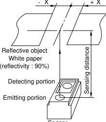
GP2D02
Compact, High Sensitive Distance
Measuring Sensor
(Unit : mm)
Features
Applications
Absolute Maximum Ratings
Parameter Symbol Rating Unit
Symbol Rating Unit
Operating Supply Voltage
Outline Dimensions
Emitting portion Detecting portion
JAPAN SOLDERLESS TERMINAL MSG. CO.
made connector (S4B-ZR) The dimensions marked withas the dimensions of lens center position.❈ are described
Block Diagram
Signal processing circuit
LED drive circuit Control circuit
Reflective object
IR LED (Control signal
input)
*1
*1 Open drain operation input
Supply voltage Input terminal voltage Output terminal voltage Operating temperature Storage temperature
1. Impervious to color and reflectivity of reflective object 2. High precision distance measurement output for direct
connection to microcomputer
4. Capable of changing of distance measuring range through change the optical portion (lens)
1. Sanitary sensors
2. Human body sensors for consumer products such as electric fans and air conditioners
3. Garage sensors
* PSD : Position Sensitive Detector
Light detector (PSD*)
BVO
3. Low dissipation current at OFF-state
(dissipation current at OFF-state : TYP. 3µA)
CC (Ta=25˚C, V =5V)
data books, etc. Contact SHARP in order to obtain the latest version of the device specification sheets before using any SHARP's device.”
“In the absence of confirmation by device specification sheets, SHARP takes no responsibility for any defects that occur in equipment using any of SHARP's devices, shown in catalogs,
■ ■
■
■
GP2D02
70ms
0.1ms 0.1ms
1.6ms 2ms
(Ta=25˚C,Vcc=5V)
Electro-optical Characteristics
Note) L : Distance to reflective object
*1 Reflective object : White paper (reflectivity : 90%)
*3 Vin terminal : Open drain drive input.
Conditions : Vin terminal current at Vin OFF-state : -1µA Vin terminal current at Vin ON-state : 0.3V
*2 Average dissipation current value during distance measuring operation when detecting of input signal, Vin as shown in the timing chart
Test Circuit
1. Test circuit
2. Vin input signal for measurement
1
2 3
4
Distance measuring sensor
8-bit serial output read
V signal inputin
DEC : Decimalized value of sensor output (8-bit serial)
Parameter Symbol Conditions MIN. TYP. MAX. Unit
Distance measuring range ∆L *1 10 - 80 cm
Output terminal voltage VOH Output voltage at High L = 20cm
*1
VCC- 0.3 - - V
VOL Output voltage at Low - - 0.3 V
Distance characteristics of output D L = 80cm, *1 - 75 - DEC
∆D Output change at L=80 cm to 20 cm, *1 48 58 68 DEC Dissipation current at operating ICC L = 20cm, *1, *2 - 22 35 mA
at OFF-state Ioff L = 20cm, *1 - 3 8 µA
Vin terminal current Ivin Vin = 0V - - 170 - 280 µA
■
GP2D02
Fig. 1 Distance Measuring Output vs. Distance to Reflective Object Timing Chart
0 20 40 60 80 100 120 160 180 200 220
140
0 20 40 60 80 100 120 140
Gray White
Distance measuring output (DEC)
Distance to reflective object L (cm)
White paper : KODAK made gray chart R-27, white surface (reflectivity : 90%) Gray paper : KODAK made gray chart R-27,
gray surface (reflectivity : 18%)
MSB LSB LSB
70ms or more 0.2ms or less1ms or more
1.5ms or more 1.5ms or more
Power OFF Vin
Output
Example of distance measuring output (8-bit)
GP2D02
Fig. 3 Detection Distance vs. Illuminance
Detection distance L (cm)
Illuminance (lx)
Test Method for Anti External Disturbing Light Characteristics
Test Method for Sensing Range Characteristics
Reflective object
Distance to reflective object
Sensor
Sunlight Illuminance meter
Fig. 2 Detection Distance vs. Sensing Range
Detection distance L (cm)
Sensing range X (mm)
KODAK made white paper (reflectivity : 90%)
Sensor Emitting portion
Detecting portion White paper (reflectivity : 90%)
Reflective object
Sensing distance
- X +X
0 5000 10000 15000 20000 25000 30000 0
10 20 30 40 50 60 70 80 90 100
50cm
30cm
15cm
- 100 - 50 0 50 100 0
10 20 30 40 50 60 70 80 90 100
Sensing distance : 80 cm
Sensing distance : 50 cm
LM555
Timer
General Description
The LM555 is a highly stable device for generating accurate time delays or oscillation. Additional terminals are provided for triggering or resetting if desired. In the time delay mode of operation, the time is precisely controlled by one external re-sistor and capacitor. For astable operation as an oscillator, the free running frequency and duty cycle are accurately controlled with two external resistors and one capacitor. The circuit may be triggered and reset on falling waveforms, and the output circuit can source or sink up to 200mA or drive TTL circuits.
Features
n Direct replacement for SE555/NE555
n Timing from microseconds through hours
n Operates in both astable and monostable modes
n Adjustable duty cycle
n Output can source or sink 200 mA
n Output and supply TTL compatible
n Temperature stability better than 0.005% per ˚C
n Normally on and normally off output
n Available in 8-pin MSOP package
Applications
n Precision timing
n Pulse generation
n Sequential timing
n Time delay generation
n Pulse width modulation n Pulse position modulation n Linear ramp generator
Schematic Diagram
DS007851-1
February 2000
LM555
T
imer
Connection Diagram
Ordering Information
Package Part Number Package Marking Media Transport NSC Drawing
8-Pin SOIC LM555CM LM555CM Rails
M08A LM555CMX LM555CM 2.5k Units Tape and Reel
8-Pin MSOP LM555CMM Z55 1k Units Tape and Reel
MUA08A LM555CMMX Z55 3.5k Units Tape and Reel
8-Pin MDIP LM555CN LM555CN Rails N08E
Dual-In-Line, Small Outline and Molded Mini Small Outline Packages
DS007851-3
Top View
LM555
Absolute Maximum Ratings
(Note 2)If Military/Aerospace specified devices are required, please contact the National Semiconductor Sales Office/ Distributors for availability and specifications.
Supply Voltage +18V
Power Dissipation (Note 3)
LM555CM, LM555CN 1180 mW
LM555CMM 613 mW
Operating Temperature Ranges
LM555C 0˚C to +70˚C
Storage Temperature Range −65˚C to +150˚C
Soldering Information Dual-In-Line Package
Soldering (10 Seconds) 260˚C Small Outline Packages
(SOIC and MSOP)
Vapor Phase (60 Seconds) 215˚C Infrared (15 Seconds) 220˚C See AN-450 “Surface Mounting Methods and Their Effect on Product Reliability” for other methods of soldering surface mount devices.
Electrical Characteristics
(Notes 1, 2) (TA= 25˚C, VCC= +5V to +15V, unless othewise specified)Parameter Conditions Limits Units
LM555C
Min Typ Max
Supply Voltage 4.5 16 V
Supply Current VCC= 5V, RL=∞ VCC= 15V, RL=∞
(Low State) (Note 4)
3 10
6
15 mA
Timing Error, Monostable
Initial Accuracy 1 %
Drift with Temperature RA= 1k to 100kΩ, 50 ppm/˚C
C = 0.1µF, (Note 5)
Accuracy over Temperature 1.5 %
Drift with Supply 0.1 %/V
Timing Error, Astable
Initial Accuracy 2.25 %
Drift with Temperature RA, RB= 1k to 100kΩ, 150 ppm/˚C
C = 0.1µF, (Note 5)
Accuracy over Temperature 3.0 %
Drift with Supply 0.30 %/V
Threshold Voltage 0.667 x VCC
Trigger Voltage VCC= 15V 5 V
VCC= 5V 1.67 V
Trigger Current 0.5 0.9 µA
Reset Voltage 0.4 0.5 1 V
Reset Current 0.1 0.4 mA
Threshold Current (Note 6) 0.1 0.25 µA
Control Voltage Level VCC= 15V
VCC= 5V
9 2.6
10 3.33
11
4 V
Pin 7 Leakage Output High 1 100 nA
Pin 7 Sat (Note 7)
Output Low VCC= 15V, I7= 15mA 180 mV
Output Low VCC= 4.5V, I7 = 4.5mA 80 200 mV
LM555
Electrical Characteristics
(Notes 1, 2) (Continued) (TA= 25˚C, VCC = +5V to +15V, unless othewise specified)Parameter Conditions Limits Units
LM555C
Min Typ Max
Output Voltage Drop (Low) VCC= 15V
ISINK= 10mA 0.1 0.25 V
ISINK= 50mA 0.4 0.75 V
ISINK= 100mA 2 2.5 V
ISINK= 200mA 2.5 V
VCC= 5V
ISINK= 8mA V
ISINK= 5mA 0.25 0.35 V
Output Voltage Drop (High) ISOURCE= 200mA, VCC= 15V 12.5 V
ISOURCE= 100mA, VCC= 15V 12.75 13.3 V
VCC= 5V 2.75 3.3 V
Rise Time of Output 100 ns
Fall Time of Output 100 ns
Note 1: All voltages are measured with respect to the ground pin, unless otherwise specified.
Note 2: Absolute Maximum Ratings indicate limits beyond which damage to the device may occur. Operating Ratings indicate conditions for which the device is func-tional, but do not guarantee specific performance limits. Electrical Characteristics state DC and AC electrical specifications under particular test conditions which guar-antee specific performance limits. This assumes that the device is within the Operating Ratings. Specifications are not guarguar-anteed for parameters where no limit is given, however, the typical value is a good indication of device performance.
Note 3: For operating at elevated temperatures the device must be derated above 25˚C based on a +150˚C maximum junction temperature and a thermal resistance of 106˚C/W (DIP), 170˚C/W (S0-8), and 204˚C/W (MSOP) junction to ambient.
Note 4: Supply current when output high typically 1 mA less at VCC= 5V. Note 5: Tested at VCC= 5V and VCC= 15V.
Note 6: This will determine the maximum value of RA+ RBfor 15V operation. The maximum total (RA+ RB) is 20MΩ. Note 7: No protection against excessive pin 7 current is necessary providing the package dissipation rating will not be exceeded.
Note 8: Refer to RETS555X drawing of military LM555H and LM555J versions for specifications.
LM555
Typical Performance Characteristics
Minimuim Pulse Width Required for Triggering
DS007851-4
Supply Current vs. Supply Voltage
DS007851-19
High Output Voltage vs. Output Source Current
DS007851-20
Low Output Voltage vs. Output Sink Current
DS007851-21
Low Output Voltage vs. Output Sink Current
DS007851-22
Low Output Voltage vs. Output Sink Current
DS007851-23
LM555
Typical Performance Characteristics
(Continued)Output Propagation Delay vs. Voltage Level of Trigger Pulse
DS007851-24
Output Propagation Delay vs. Voltage Level of Trigger Pulse
DS007851-25
Discharge Transistor (Pin 7) Voltage vs. Sink Current
DS007851-26
Discharge Transistor (Pin 7) Voltage vs. Sink Current
DS007851-27
LM555
Applications Information
MONOSTABLE OPERATIONIn this mode of operation, the timer functions as a one-shot (Figure 1). The external capacitor is initially held discharged by a transistor inside the timer. Upon application of a nega-tive trigger pulse of less than 1/3 VCCto pin 2, the flip-flop is
set which both releases the short circuit across the capacitor and drives the output high.
The voltage across the capacitor then increases exponen-tially for a period of t = 1.1 RAC, at the end of which time the voltage equals 2/3 VCC. The comparator then resets the
flip-flop which in turn discharges the capacitor and drives the output to its low state.Figure 2 shows the waveforms gener-ated in this mode of operation. Since the charge and the threshold level of the comparator are both directly propor-tional to supply voltage, the timing internal is independent of supply.
During the timing cycle when the output is high, the further application of a trigger pulse will not effect the circuit so long as the trigger input is returned high at least 10µs before the end of the timing interval. However the circuit can be reset during this time by the application of a negative pulse to the reset terminal (pin 4). The output will then remain in the low state until a trigger pulse is again applied.
When the reset function is not in use, it is recommended that it be connected to VCCto avoid any possibility of false
trig-gering.
Figure 3 is a nomograph for easy determination of R, C val-ues for various time delays.
NOTE:In monostable operation, the trigger should be driven high before the end of timing cycle.
ASTABLE OPERATION
If the circuit is connected as shown inFigure 4 (pins 2 and 6 connected) it will trigger itself and free run as a multivibrator. The external capacitor charges through RA+ RBand
dis-charges through RB. Thus the duty cycle may be precisely
set by the ratio of these two resistors.
In this mode of operation, the capacitor charges and dis-charges between 1/3 VCCand 2/3 VCC. As in the triggered
mode, the charge and discharge times, and therefore the fre-quency are independent of the supply voltage.
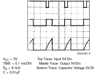
DS007851-5
FIGURE 1. Monostable
DS007851-6
VCC= 5V Top Trace: Input 5V/Div. TIME = 0.1 ms/DIV. Middle Trace: Output 5V/Div. RA= 9.1kΩ Bottom Trace: Capacitor Voltage 2V/Div. C = 0.01µF
FIGURE 2. Monostable Waveforms
DS007851-7
FIGURE 3. Time Delay
DS007851-8
FIGURE 4. Astable
LM555
Applications Information
(Continued) Figure 5 shows the waveforms generated in this mode of operation.The charge time (output high) is given by: t1= 0.693 (RA+ RB) C
And the discharge time (output low) by: t2= 0.693 (RB) C
Thus the total period is:
T = t1+ t2= 0.693 (RA+2RB) C
The frequency of oscillation is:
Figure 6 may be used for quick determination of these RC values.
The duty cycle is:
FREQUENCY DIVIDER
The monostable circuit ofFigure 1 can be used as a fre-quency divider by adjusting the length of the timing cycle. Figure 7 shows the waveforms generated in a divide by three circuit.
PULSE WIDTH MODULATOR
When the timer is connected in the monostable mode and triggered with a continuous pulse train, the output pulse width can be modulated by a signal applied to pin 5.Figure 8 shows the circuit, and in Figure 9 are some waveform examples.
DS007851-9
VCC= 5V Top Trace: Output 5V/Div.
TIME = 20µs/DIV. Bottom Trace: Capacitor Voltage 1V/Div. RA= 3.9kΩ
RB= 3kΩ C = 0.01µF
FIGURE 5. Astable Waveforms
DS007851-10
FIGURE 6. Free Running Frequency
DS007851-11
VCC= 5V Top Trace: Input 4V/Div. TIME = 20µs/DIV. Middle Trace: Output 2V/Div. RA= 9.1kΩ Bottom Trace: Capacitor 2V/Div. C = 0.01µF
FIGURE 7. Frequency Divider
DS007851-12
FIGURE 8. Pulse Width Modulator
DS007851-13
VCC= 5V Top Trace: Modulation 1V/Div. TIME = 0.2 ms/DIV. Bottom Trace: Output Voltage 2V/Div. RA= 9.1kΩ
C = 0.01µF
FIGURE 9. Pulse Width Modulator
LM555
Applications Information
(Continued)PULSE POSITION MODULATOR
This application uses the timer connected for astable opera-tion, as inFigure 10, with a modulating signal again applied to the control voltage terminal. The pulse position varies with the modulating signal, since the threshold voltage and hence the time delay is varied. Figure 11 shows the waveforms generated for a triangle wave modulation signal.
LINEAR RAMP
When the pullup resistor, RA, in the monostable circuit is
re-placed by a constant current source, a linear ramp is gener-ated.Figure 12 shows a circuit configuration that will perform this function.
Figure 13 shows waveforms generated by the linear ramp. The time interval is given by:
VBE.0.6V
DS007851-14
FIGURE 10. Pulse Position Modulator
DS007851-15
VCC= 5V Top Trace: Modulation Input 1V/Div. TIME = 0.1 ms/DIV. Bottom Trace: Output 2V/Div. RA= 3.9kΩ
RB= 3kΩ C = 0.01µF
FIGURE 11. Pulse Position Modulator
DS007851-16
FIGURE 12.
DS007851-17
VCC= 5V Top Trace: Input 3V/Div. TIME = 20µs/DIV. Middle Trace: Output 5V/Div. R1= 47kΩ Bottom Trace: Capacitor Voltage 1V/Div. R2= 100kΩ
RE= 2.7 kΩ C = 0.01 µF
FIGURE 13. Linear Ramp
LM555
Applications Information
(Continued)50% DUTY CYCLE OSCILLATOR
For a 50% duty cycle, the resistors RAand RBmay be
con-nected as inFigure 14. The time period for the output high is the same as previous, t1= 0.693 RAC. For the output low it
is t2 =
Thus the frequency of oscillation is
Note that this circuit will not oscillate if RBis greater than 1/2 RAbecause the junction of RAand RBcannot bring pin 2 down to 1/3 VCCand trigger the lower comparator.
ADDITIONAL INFORMATION
Adequate power supply bypassing is necessary to protect associated circuitry. Minimum recommended is 0.1µF in par-allel with 1µF electrolytic.
Lower comparator storage time can be as long as 10µs when pin 2 is driven fully to ground for triggering. This limits the monostable pulse width to 10µs minimum.
Delay time reset to output is 0.47µs typical. Minimum reset pulse width must be 0.3µs, typical.
Pin 7 current switches within 30ns of the output (pin 3) volt-age.
DS007851-18
FIGURE 14. 50% Duty Cycle Oscillator
LM555
Physical Dimensions
inches (millimeters) unless otherwise notedSmall Outline Package (M) NS Package Number M08A
8-Lead (0.118” Wide) Molded Mini Small Outline Package NS Package Number MUA08A
LM555
Physical Dimensions
inches (millimeters) unless otherwise noted (Continued)LIFE SUPPORT POLICY
NATIONAL’S PRODUCTS ARE NOT AUTHORIZED FOR USE AS CRITICAL COMPONENTS IN LIFE SUPPORT DEVICES OR SYSTEMS WITHOUT THE EXPRESS WRITTEN APPROVAL OF THE PRESIDENT AND GENERAL COUNSEL OF NATIONAL SEMICONDUCTOR CORPORATION. As used herein:
1. Life support devices or systems are devices or systems which, (a) are intended for surgical implant into the body, or (b) support or sustain life, and whose failure to perform when properly used in accordance with instructions for use provided in the labeling, can be reasonably expected to result in a significant injury to the user.
2. A critical component is any component of a life support device or system whose failure to perform can be reasonably expected to cause the failure of the life support device or system, or to affect its safety or effectiveness.
National Semiconductor Corporation
Americas Tel: 1-800-272-9959 Fax: 1-800-737-7018 Email: [email protected]
National Semiconductor Europe
Fax: +49 (0) 180-530 85 86 Email: [email protected] Deutsch Tel: +49 (0) 69 9508 6208 English Tel: +44 (0) 870 24 0 2171 Français Tel: +33 (0) 1 41 91 8790
National Semiconductor Asia Pacific Customer Response Group
Tel: 65-2544466 Fax: 65-2504466 Email: [email protected]
National Semiconductor Japan Ltd.
Tel: 81-3-5639-7560 Fax: 81-3-5639-7507 www.national.com
Molded Dual-In-Line Package (N) NS Package Number N08E
LM555
T
imer
1996 Microchip Technology Inc. DS30430B-page 1
Devices Included in this Data Sheet:
• PIC16F83 • PIC16CR83 • PIC16F84 • PIC16CR84
• Extended voltage range devices available
(PIC16LF8X, PIC16LCR8X)
High Performance RISC CPU Features:
• Only 35 single word instructions to learn • All instructions single cycle (400 ns @ 10 MHz)
except for program branches which are two-cycle • Operating speed: DC - 10 MHz clock input
DC - 400 ns instruction cycle
• 14-bit wide instructions • 8-bit wide data path
• 15 special function hardware registers • Eight-level deep hardware stack
• Direct, indirect and relative addressing modes • Four interrupt sources:
- External RB0/INT pin - TMR0 timer overflow
- PORTB<7:4> interrupt on change - Data EEPROM write complete • 1,000,000 data memory EEPROM
ERASE/WRITE cycles
• EEPROM Data Retention > 40 years
Peripheral Features:
• 13 I/O pins with individual direction control • High current sink/source for direct LED drive
- 25 mA sink max. per pin - 20 mA source max. per pin • TMR0: 8-bit timer/counter with 8-bit
programmable prescaler
Flash RAM EEPROM
PIC16F83 512 words 36 64 10 MHz
PIC16CR83 512 words 36 64 10 MHz
PIC16F84 1 K-words 68 64 10 MHz
PIC16CR84 1 K-words 68 64 10 MHz
F = Flash; CR = ROM
Pin Diagram
Special Microcontroller Features:
• Power-on Reset (POR) • Power-up Timer (PWRT) • Oscillator Start-up Timer (OST)
• Watchdog Timer (WDT) with its own on-chip RC oscillator for reliable operation
• Code-protection
• Power saving SLEEP mode • Selectable oscillator options
• Serial In-System Programming - via two pins (ROM devices support only Data EEPROM programming)
CMOS Technology:
• Low-power, high-speed CMOS Flash/EEPROM technology
• Fully static design
• Wide operating voltage range: - Commercial: 2.0V to 6.0V
- Industrial: 2.0V to 6.0V
• Low power consumption: - < 2 mA typical @ 5V, 4 MHz
8-Bit CMOS Flash/EEPROM Microcontrollers
PIC16F8X
DS30430B-page 2 1996 Microchip Technology Inc.
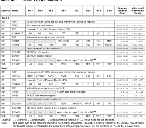
Table of Contents
1.0 General Description ... 3
2.0 PIC16F8X Device Varieties ... 5
3.0 Architectural Overview... 7
4.0 Memory Organization ... 11
5.0 I/O Ports... 21
6.0 Timer0 Module and TMR0 Register... 27
7.0 Data EEPROM Memory... 33
8.0 Special Features of the CPU ... 37
9.0 Instruction Set Summary ... 55
10.0 Development Support ... 67
11.0 Electrical Characteristics for PIC16F83 and PIC16F84... 71
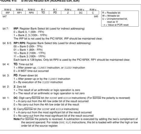
12.0 DC & AC Characteristics Graphs/Tables for PIC16F83 and PIC16F84 ... 83
13.0 Electrical Characteristics for PIC16CR83 and PIC16CR84... 85
14.0 DC & AC Characteristics Graphs/Tables for PIC16CR83 and PIC16CR84 ... 97
15.0 Packaging Information ... 99
Appendix A: Feature Improvements ... 103
Appendix B: Compatibility... 103
Appendix C: What’s New ... 104
Appendix D: What’s Changed... 104 Appendix E: PIC16C84 to PIC16F83/CR83 and PIC16F84/CR84 Conversion Considerations... 104 Appendix F: PIC16/17 Microcontrollers ... 105 Index... 115 PIC16F8X Product Identification System ... 121
To Our Valued Customers
1996 Microchip Technology Inc. DS30430B-page 3
PIC16F8X
1.0
GENERAL DESCRIPTION
The PIC16F8X is a group in the PIC16CXX family of low-cost, high-performance, CMOS, fully-static, 8-bit microcontrollers. This group contains the following devices:
• PIC16F83 • PIC16CR83 • PIC16F84 • PIC16CR84
All PIC16/17 microcontrollers employ an advanced RISC architecture. PIC16CXX devices have enhanced core features, eight-level deep stack, and multiple internal and external interrupt sources. The separate instruction and data buses of the Harvard architecture allow a 14-bit wide instruction word with a separate 8-bit wide data bus. The two stage instruction pipeline allows all instructions to execute in a single cycle, except for program branches (which require two cycles). A total of 35 instructions (reduced instruction set) are available. Additionally, a large register set is used to achieve a very high performance level.
PIC16F8X microcontrollers typically achieve a 2:1 code compression and up to a 2:1 speed improvement (at 10 MHz) over other 8-bit microcontrollers in their class.
The PIC16F8X has up to 68 bytes of RAM, 64 bytes of Data EEPROM memory, and 13 I/O pins. A timer/counter is also available.
The PIC16CXX family has special features to reduce external components, thus reducing cost, enhancing system reliability and reducing power consumption. There are four oscillator options, of which the single pin RC oscillator provides a low-cost solution, the LP oscillator minimizes power consumption, XT is a standard crystal, and the HS is for High Speed crystals. The SLEEP (power-down) mode offers power saving. The user can wake the chip from sleep through several external and internal interrupts and resets.
A highly reliable Watchdog Timer with its own on-chip RC oscillator provides protection against software lock-up.
The devices with Flash program memory allow the same device package to be used for prototyping and production. In-circuit reprogrammability allows the code to be updated without the device being removed from the end application. This is useful in the development of many applications where the device may not be easily accessible, but the prototypes may require code updates. This is also useful for remote applications where the code may need to be updated (such as rate information).
Table 1-1 lists the features of the PIC16F8X, and Appendix D: list the features of all of the Microchip microcontrollers.
A simplified block diagram of the PIC16F8X is shown in Figure 3-1.
The PIC16F8X fits perfectly in applications ranging from high speed automotive and appliance motor control to low-power remote sensors, electronic locks, security devices and smart cards. The Flash/EEPROM technology makes customization of application programs (transmitter codes, motor speeds, receiver frequencies, security codes, etc.) extremely fast and convenient. The small footprint packages make this microcontroller series perfect for all applications with space limitations. Low-cost, low-power, high performance, ease of use and I/O flexibility make the PIC16F8X very versatile even in areas where no microcontroller use has been considered before (e.g., timer functions, serial communication, capture and compare, PWM functions and co-processor applications).
The serial in-system programming feature (via two pins) offers flexibility of customizing the product after complete assembly and testing. This feature can be used to serialize a product, store calibration data, or program the device with the current firmware before shipping.
1.1
Family and Upward Compatibility
Those users familiar with the PIC16C5X family of microcontrollers will realize that this is an enhanced version of the PIC16C5X architecture. Please refer to Appendix A: for a detailed list of enhancements. Code written for PIC16C5X can be easily ported to the PIC16F8X (Appendix B:).
1.2
Development Support
The PIC16CXX family is supported by a full-featured macro assembler, a software simulator, an in-circuit emulator, a low-cost development programmer and a full-featured programmer. A “C” compiler and fuzzy logic support tools are also available.
PIC16F8X
DS30430B-page 4 1996 Microchip Technology Inc.
TABLE 1-1:
PIC16F8X FAMILY OF DEVICES
PIC16C84 10 — 1K — 36 64 TMR0 4 13 2.0-6.0 18-pin DIP, SOIC
PIC16F84(1) 10 1K — — 68 64 TMR0 4 13 2.0-6.0 18-pin DIP, SOIC
PIC16CR84(1) 10 — — 1K 68 64 TMR0 4 13 2.0-6.0 18-pin DIP, SOIC
PIC16F83(1) 10 512 — — 36 64 TMR0 4 13 2.0-6.0 18-pin DIP, SOIC
PIC16CR83(1) 10 — — 512 36 64 TMR0 4 13 2.0-6.0 18-pin DIP, SOIC
All PIC16/17 family devices have Power-on Reset, selectable Watchdog Timer, selectable code protect, and high I/O current capability.
All PIC16C8X family devices use serial programming with clock pin RB6 and data pin RB7. Note 1: Please contact your local sales office for availability of these devices.
Maximum Frequency of Operation (MHz)EEPROM Data Memory (bytes)Data EEPROM (bytes)Timer Module(s)Interrupt SourcesI/O Pins Voltage Range (Volts)Packages
Program Memory
Clock Memory Peripherals Features
ROM
1996 Microchip Technology Inc. DS30430B-page 5
PIC16F8X
2.0
PIC16F8X DEVICE VARIETIES
A variety of frequency ranges and packaging options are available. Depending on application and production requirements the proper device option can be selected using the information in this section. When placing orders, please use the “PIC16F8X Product Identification System” at the back of this data sheet to specify the correct part number.
There are four device “types” as indicated in the device number.
1. F, as in PIC16F84. These devices have Flash
program memory and operate over the standard voltage range.
2. LF, as in PIC16LF84. These devices have Flash
program memory and operate over an extended voltage range.
3. CR, as in PIC16CR83. These devices have
ROM program memory and operate over the standard voltage range.
4. LCR, as in PIC16LCR84. These devices have
ROM program memory and operate over an extended voltage range.
When discussing memory maps and other architectural
features, the use of F and CR also implies the LF and
LCR versions.
2.1
Electrically Erasable Devices
These devices are offered in the lower cost plastic package, even though the device can be erased and reprogrammed. This allows the same device to be used for prototype development and pilot programs as well as production.
A further advantage of the electrically erasable version is that they can be erased and reprogrammed in-circuit,
or by device programmers, such as Microchip's PICSTART Plus or PRO MATE II programmers.
2.2
Quick-Turnaround-Production (QTP)
Devices
Microchip offers a QTP Programming Service for factory production orders. This service is made available for users who choose not to program a medium to high quantity of units and whose code patterns have stabilized. The devices have all Flash locations and configuration options already pro-grammed by the factory. Certain code and prototype verification procedures do apply before production shipments are available.
For information on submitting a QTP code, please contact your Microchip Regional Sales Office.
2.3
Serialized
Quick-Turnaround-Production
(SQTP
) Devices
Microchip offers the unique programming service where a few user-defined locations in each device are programmed with different serial numbers. The serial numbers may be random, pseudo-random or sequential.
Serial programming allows each device to have a unique number which can serve as an entry-code, password or ID number.
For information on submitting a SQTP code, please contact your Microchip Regional Sales Office.
2.4
ROM Devices
Some of Microchip’s devices have a corresponding device where the program memory is a ROM. These devices give a cost savings over Microchip’s traditional user programmed devices (EPROM, EEPROM).
ROM devices (PIC16CR8X) do not allow serialization information in the program memory space. The user may program this information into the Data EEPROM.
For information on submitting a ROM code, please contact your Microchip Regional Sales Office.
SM
PIC16F8X
DS30430B-page 6 1996 Microchip Technology Inc.