Informasi Dokumen
- Penulis:
- Larry D. Smith
- Eric Bogatin
- Sekolah: Pearson Education
- Mata Pelajaran: Power Integrity
- Topik: Principles of Power Integrity for PDN Design—Simplified Robust and Cost Effective Design for High Speed Digital Products
- Tipe: book
- Tahun: 2017
- Kota: Boston
Ringkasan Dokumen
I. Engineering the Power Delivery Network
The Power Delivery Network (PDN) is critical for ensuring that high-speed digital products operate reliably. It encompasses the entire path from voltage regulator modules (VRMs) to the circuits on the chip, including power and ground planes, connectors, and capacitors. Understanding the PDN is essential because it plays a vital role in distributing low-noise DC voltage and power to active devices while also providing a return path for signals. Poorly designed PDNs can lead to increased voltage noise, which can adversely affect signal integrity and overall system performance.
1.1 What Is the Power Delivery Network (PDN) and Why Should I Care?
The PDN is a network of interconnects that deliver power from the VRM to the active components on a board. Its primary purpose is to maintain a stable, low-noise power supply. Voltage noise in the PDN can lead to functional failures, increased bit error ratios, and timing issues in high-speed digital circuits. Understanding the layout and impedance characteristics of the PDN is essential for engineers to ensure that the system functions correctly under varying load conditions.
1.2 Engineering the PDN
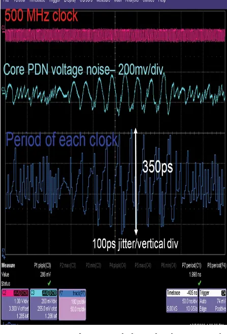
Effective PDN design requires maintaining voltage noise within acceptable limits, typically around ±5% of the supply voltage. This involves selecting a VRM with low noise characteristics and designing the PDN to minimize impedance. The PDN's impedance profile directly affects the voltage noise seen by the circuits, which is crucial for high-frequency applications. Engineers must analyze the current spectrum and impedance profile to ensure that the voltage noise remains below specified thresholds, thereby preventing performance degradation.
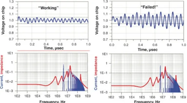
1.3 “Working” or “Robust” PDN Design
A robust PDN design ensures that the system can handle varying operational conditions without failing. This involves setting a target impedance that accounts for the worst-case transient current and the maximum allowable voltage noise. A PDN that consistently stays below this target impedance will minimize the risk of voltage noise exceeding acceptable limits, thus ensuring reliable operation across different software loads and operational scenarios. The design must account for potential variations in current demands and their impact on the PDN performance.
II. Essential Principles of Impedance for PDN Design
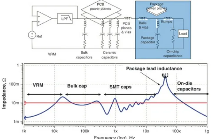
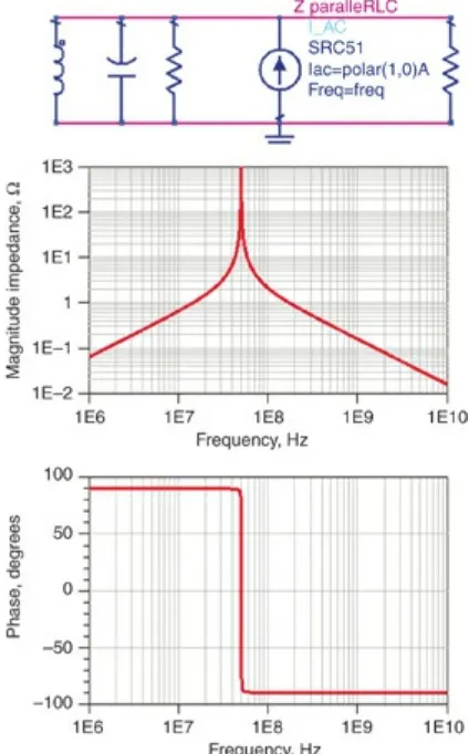
Impedance is a fundamental concept in PDN design, influencing how effectively power is delivered to circuits. Understanding the frequency-dependent behavior of impedance is essential for evaluating and optimizing PDN performance. Engineers must consider both series and parallel RLC circuits to analyze the overall impedance profile. The goal is to minimize impedance peaks that could contribute to excessive voltage noise during transient events, which can occur when circuits switch states rapidly.
2.1 Why Do We Care About Impedance?
Impedance affects how voltage noise propagates through the PDN. High impedance can lead to significant voltage drops during transient events, which can adversely impact the performance of sensitive digital circuits. Understanding the impedance characteristics allows engineers to design more effective decoupling strategies and optimize the placement of capacitors to achieve a low-impedance path for power delivery.
2.2 Impedance in the Frequency Domain
The impedance profile of a PDN varies with frequency, making it essential to analyze it in the frequency domain. Engineers must consider how different components, such as capacitors and inductors, interact at various frequencies to shape the overall impedance. This analysis helps in identifying critical frequencies where impedance peaks occur, allowing for targeted design improvements to mitigate voltage noise.
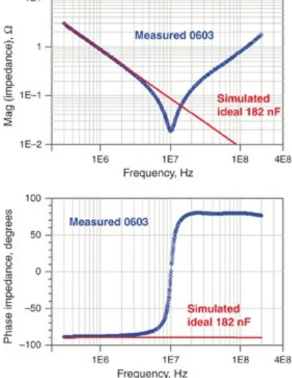
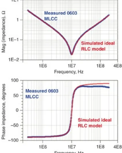
2.3 Calculating or Simulating Impedance
Calculating or simulating the impedance of the PDN can be accomplished using tools like SPICE simulators. These simulations provide insights into the expected impedance profile under different loading conditions. By modeling the PDN, engineers can predict how changes in component values or configurations will affect overall performance, enabling them to optimize designs before physical prototyping.
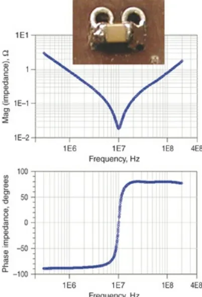
III. Measuring Low Impedance
Measuring low impedance accurately is crucial for validating PDN designs. Techniques such as the V/I definition of impedance and vector network analyzers (VNAs) are employed to obtain precise measurements. Engineers must be aware of the limitations and potential artifacts introduced during measurements, particularly at low frequencies, to ensure that the data accurately reflects the PDN's performance characteristics.
3.1 Why Do We Care About Measuring Low Impedance?
Accurate measurement of low impedance is essential for confirming that the PDN meets design specifications. High-frequency applications often require impedances in the milliohm range, where small variations can significantly impact performance. Understanding how to measure and interpret these low impedance values is critical for ensuring that the PDN design is robust and effective.
3.2 Measurements Based on the V/I Definition of Impedance
The V/I definition of impedance provides a straightforward method for measuring the impedance of a PDN by applying a known voltage and measuring the resulting current. This approach allows engineers to calculate impedance at various frequencies, helping to identify potential issues in the PDN design. However, care must be taken to minimize external influences that could skew results.
3.3 Measuring Impedance Based on the Reflection of Signals
Signal reflection techniques involve sending a signal through the PDN and analyzing the reflected signal to determine impedance characteristics. This method can be particularly useful for identifying discontinuities or impedance mismatches within the PDN. Engineers must be adept at interpreting reflection data to diagnose potential problems and optimize design.