FABRICATION OF ORGA NIC LIGHT EMITTING DIODES (OLEDs)
FOR FLAT PANEL DISPLAYS
Muhamad Mat Salleh1, Tengku Hasnan Tengku Aziz1, Suhaila Sepeai1, and Muhammad Yahaya2
1
Institute of Microengineering and Nanoelectronics (IMEN) , Universiti Kebangsaan Malaysia 43600 UKM Bangi, Selangor, MALAYSIA
2
School of Applied Physics, Faculty of Science & Technology, Universiti Kebangsaan Malaysia 43600 UKM Bangi, Selangor, MALAYSIA
email: [email protected]
ABSTRACT
Organic light emitting diodes (OLEDs) are thin film devices in which organic materials are sandwiched between two electrodes. These devices emit light when electricity is passed through them. OLEDs have gained much attention because their potential applications to full color flat panel displays. Generally, OLEDs are assembled using an heterojunction architecture between three or more organic molecular materials: an electron injection layer, the emitting one and finally the hole injection layer. There are two types of OLED devices, depend on the type of molecular materials used in the devices. The first type is Small Molecule OLED. The production of small-molecule OLEDs require vacuum deposition. The second type is Light-Emitting Polymer. In this technology, the organic thin films can be deposited by spin coating or by a technique derived from commercial inkjet printing. This paper discusses the fabrication of both types of OLEDs. A small molecule blue organic light emitting diode was fabricated using thermal evaporation system with ITO/2-TNATA/NPB/DPVBi:dopant/ Alq3/LiF/Al structure,
where the emitting molecules is 4,4’-bis(2,2’-diphenylvinyl)-1,1’-biphenyl (DPVBi). The typical brightness, the power consumption and the turn-on voltage of the device were 30 cd/m2, less than 50 mW and 5.0 V respectively. For polymer light-emitting diode, device with structure of ITO/PHF/Al structure was fabricated, where PHF is poly (4, 4’-diphenylene diphenylvinylene). This device has turn-on voltage at 23.0 V. A reduction of turn-on voltage of this device is achieved by using a nanocomposite layer consisting of PHF and SiO2 nanoparticles as the
emitting layer. A white OLED combines with colour filters is one of the approaches to obtained full colour flat screen display. White light emitting devices were fabricated with structure of ITO/PHF:rubrene/Al where the white light was optimized through variation of mixing concentrations of PHF and rubrene. The results show that the combination of 0.6 wt% PHF and 0.06 wt% rubrene produced the optimum white light at CIE coordinate of (0.31,0.31). The standard coordinate for white light is (0.33,0.33). The turn-on voltage of this device is 14.0 V and the brightness is 6541 cd/m2. The turn-on of this device was reduced to 8.0 V through an annealing process at 150°C.
Keywords : Organic light emitting diodes (OLEDs), small molecule device, polymer light-emitting diode, display.
1. INTRODUCTION
Organic light emitting diodes (OLEDs) are thin film devices in which organic materials are sandwiched between two electrodes. These devices emit light when electricity is passed through them. OLEDs have gained much attention in both academic and commercial fields because their attractive characteristics and potential applications to full color flat panel displays, such as mobile phones, PDA, etc. (Forest, 2003; Rajeswaran, et.al., 2000) Organic materials show significant potential in future display applications from small area handheld telecom devices to large area displays due to their high luminance, low fabrication costs, ease to fabricate large area devices and the ability of adjusting the emission wavelength (Hung and Chen, 2002). Since the first commercial 64×256-pixel OLED display used for car stereos was produced by Pioneer Corp. in 1997, more and more OLEDs have been made commercially by far for displays in electronic products, especially in digital products (Burrows, et.al., 1997)
Generally, OLEDs are assembled using an heterojunction architecture between three or more organic molecular materials: an electron injection layer, the emitting layer and finally the hole injection layer. There are two types of OLED devices, depend on the type of molecular materials used in the devices. The first type is Small Molecule OLED. The technology of these devices was at first developed by Eastman-Kodak (Tang, et.al., 1989). The production of small-molecule OLEDs require vacuum deposition. The second type is Light-Emitting Polymer; these devices are better known as polymer light-emitting diodes (PLEDs). The technology of these devices was developed by Cambridge Display Technologies or CDT (Greenham, et.al., 1993). In this technology, the organic thin films can be deposited by spin coating or by a technique derived from commercial inkjet printing.
Current research on OLEDs is focusing on the integration of OLEDs into full-color, flat panel displays. Prototypes have been demonstrated or reported by several research
organizations, and each of them took a different approach to the fabrication. One of the approaches is to use white OLEDs with color filter arrays. This approach does not need to pattern organic materials and is able to adopt the color filter technique used in a LCD panel (Misra, et.al., 2006). There have been many effords to develop the white OLED, such as (i) host-quess system, (ii) multilayer structures, (iii) exciplex emission structures, (iv) microcavity structures, (v) down-conversion phosphor system, and (vi) single molecule structures.
Although enormous progress has been made for OLEDs in recent years, there are still several problems need to be solved such as, improving the brightness and luminous efficiency, lowering the turn-on voltage, and increasing the lifetime of devices. From a view of materials these problems can be solved by synthesizing new materials, but a good material for fabricating devices with high brightness, elevated efficiency and desired color purity cannot be achieved easily. In recent years, there has been increasing interest in combining the nanotechnology advances with organic devices. It is believed that the composite materials consisting of a polymer and inorganic nanostructures can exhibit improved charge transport and stability characteristics, while retaining the fabrication advantages, i.e., easy processing, low production and material cost, and possibility of fabrication of large area and/or flexible devices. Use of different organic –inorganic nanocomposites in OLEDs has been reported. Incorporation of insulating oxide nanoparticles (SiO2 or TiO2) into
electroluminescent polymer resulted in radiances of 10,000 cd/m2 with external quantum efficiencies of about 1% at 5 V. Improved efficiency and luminance for nanocomposite polymer light-emitting diodes was reported with the modification of the ITO electrode with SiO2 monolayer.
ITO/2-TNATA/NPB/DPBVi:dopant
/Alq3/LiF/Al, blue polymer of ITO/PHF/Al, and
white polymer OLEDs of ITO/PHF: rubrene/Al.
2. SMALL MOLECULE OLED
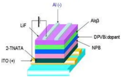
Figure. 1. The structure of small molecule OLED
Small molecule OLED is made of semiconductor organic -metal material. In this research we have fabricated a small molecule OLED consisting electron injecting layer (EIL), electron transport layer (ETL), emitting layer (EL), hole transport layer (HTL) and hole injecting layer (HIL). The structure of the device is ITO/2-TNATA/NPB/DPBVi: dopant/Alq3/LiF/Al (Figure 1), where indium
tin oxide, ITO coated on a glass substrate as an anode electrode, 4,4',4"-tris(N-(2-naphthyl)-N-phenyl-amino)-triphenylamine, 2-TNATA as
hole injection layer,
4,4'-bis(1-naphthylphenylamino)biphenyl, NPB as hole transport layer, doped 4,4'-bis-(2,2-diphenyl-vinyl)-biphenyl, DPVBi as blue emitting layer, tris-(8-hydroxyquinoline) aluminium, Alq3 as
electron transport layer, lithium fluoride, LiF as electron injection layer and Al as cathode. The multi layers device was fabricated using EL3600 OLED Fabrication System from Advanced Neotech System (ANS Inc).
The EL3600 OLED Fabrication System consist two different chambers that is organic chamber for small molecule evaporation process and metal chamber for cathode deposition. All the fabrication process was done
in an ultra high vacuum. Before the fabrication process was done, both of the chambers were purged with N2 gases to make sure the
chambers are free from any contamination. The chambers were then vacuumed to high vacuum condition.
The ITO glass substrate with pixel used in this research was undergone an ozone treatment to remove the carbon contamination before deposition process. This anode ITO was then loaded into an organic chamber to undergone organic deposition process. The organic chamber consist six organic sources with six different shutters for each of the organic sources to control the deposition process. The deposition process started with the deposition of 2-TNATA hole injection layer, followed by NPB hole transport layer. The DPVBi:dopant emitting layer was deposited by opening both of the DPVBi and dopant shutters at the same time during the deposition process. The Alq3 electron transport layer was then
deposited onto the DPVBi:dopant emitting layer followed by LiF electron injection layer.
The multilayered organics on the ITO glass substrate was then loaded into the metal chamber for cathode deposition. The separated chambers for organic and metal is because of very large different of operating deposition temperature in both type of materials. The fabricated device was then undergone a encapsulation process using the UV-resin and SiO2 tape. In the encapsulation process SiO2
tape was introduced into the aluminum mask. The SiO2 tape was functioned as water
absorbers. The aluminum mask was sealed onto the device using the UV-resin. The UV-resin will act as gum when undergone the UV-lamp.
The fabricated device emits blue light with typical brightness of 30 cd/m2. The power
consumption and the turn-on voltage of the device were less than 50 mW and 5.0 V respectively.
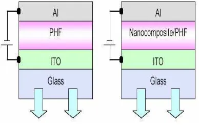
3. POLYMER LIGHT EMITTING DIODE
nanocomposite/Al were fabricated, where PHF is poly (4, 4’-diphenylene diphenyl-vinylene). The nanocomposite is consist of PHF and SiO2
nanoparticles. Figure 2 shows structutre of the PLED devices.
Figure. 2 The structure of PLED devices
The nanocomposite emitting layer of PHF and SiO2 nanoparticles were prepared
through a direct mixing of PHF solution and SiO2 nanoparticles solution. The nanoparticles
SiO2 solution were prepared by dissolve 0.014
gram of 50 nm nanoparticles commercial available SiO2 powder in 4.0 ml of ethanol,
EtOH. The solution then was stirred for 16 hours. 0.05 ml of the solution was then dropped into 11 mg/ml of PHF in toluene. The SiO2:
PHF solution was then deposited on the ITO coated glass substrate with a sheet resistance of 5 Ω/m2 using spin coating technique. The typical spinning speed and spinning time used were 3000 rpm and 40 s respectively. An aluminum layer as cathode was deposited onto the emitting layer through a mask by electron gun evaporation technique from a Molybdenum crucible at a chamber pressure of 2.5 x 10⁻⁵ mbar, yielding active areas of 0.71 cm2. The current-voltage of the device was measured using Keithley 238 source measure unit. The electroluminescent spectra were measured by HR2000 Ocean Optic spectrometer. All measurement was done at the room temperature. The devices heterostructurue was studie d using a Scanning Electron Microscopy, SEM. The photoluminescence properties of the
nanocomposite thin films were measured using the Perkin Elmer LS 55 Luminescence Spectrometer.
The photoluminescence spectra of PHF and PHF-SiO2 nanocomposites thin films
showed that the form and position of peaks in the spectra curves for both films are almost similar, except that the intensity for nanocomposites film is higher. This indicates that the presence of transparent SiO2
nanoparticles do not affected the optical properties of organic PHF polymer. However, the SiO2 nanoparticles have increased the
number of PHF molecules deposited in the film, since they provide more deposition surface area and this has contribute to photoluminescence increment. This was further confirmed with the electrolumine-scence curves of the devices where the nanocomposites device has higher intensity. The electroluminescent spectra also
indicated that the presence of SiO2
nanoparticles in the PHF do not change the emitted colour of the device.
The current-voltage (I-V) characteris-tics of the fabricated devices were studied. The turn-on voltages estimated from the I-V curves were 23.0 V and 18.0 V for the ITO/PHF/Al device and the nanocomposites device respectively.
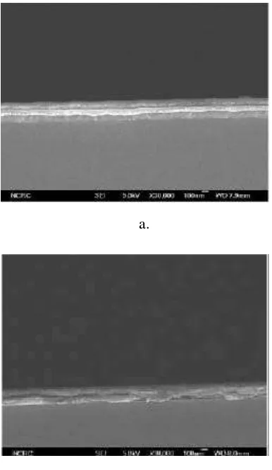
The SEM images show that the nanocomposite SiO2:PHF sample have a good adhesion an uniform surface compared to the PHF sample (Figure 3).
a.
b.
Figure 3. The SEM images shows the (a) nanocomposite SiO2:PHF (b) the PHF sample
4. POLYMER LIGHT EMITTING DIODE (WHITE LIGHT)
Current research on OLEDs is focusing on the integration of OLEDs into full colour, flat panel display and one of the approaches is to use white OLEDs with colour filter array. We have fabricated single layer OLED devices that utilized an emitting layer consisting PHF as blue light emitting host and 5,6,11,12-tetraphenyl-napthacene, rubrene as red-orange dopant. (Figure 4). The white emitting devices were obtained through variation of rubrene concentration. Table 1 summarizes the results
from CIE coordinates measurement. The white point in CIE coordinates system is defined as (0.33, 0.33). The nearest white emission was obtained in the device with 0.06 wt% rubrene where its CIE coordinates is (0.3, 0.33).
Although we have successful obtained a white light emitting devices, we found that the devices have high turn-on voltage, in the range of 14.0 V - 18.0 V. An attempt to reduce turn-on voltage of the devices was made through annealing process. The annealing process of the devices was done at 50 °C, 100 °C and 150 °C.
.
Figure 4. ITO/PHF:rubrene/Al structure
5. CONCLUSIONS
In summary both type of small molecule OLEDs and polymer OLEDs have their own advantages and disadantages. nOLEDs have bright future for the display and lightin g industries.
Understanding the nanostructures of the thin films and contact between layers of the devices are very important to improve the performance of the devices
.
REFERENCES
Burrows, P. E., S. R. Forrest, and M. E. Thompson, 1997. Prospects and applications for organic light-emitting devices. Current Opinion in Solid State and Materials Science, 2(2): 236-243. Forest, S. R., 2003. The road to high efficiency
organic light emitting devices. Organic Electronics, 4 (2-3): 45-48.
Greenham, N. C., S. C. Moratti, D. D. C. Bradley, R. H. Friend, and A.
B. Holmes, 1993. Efficient light-emitting diodes based on polymers with high electron affinities. Nature, 365: 628 – 630.
Hung L. S., and C. H. Chen, 2002. Recent progress of molecular organic electrolu minescent materials and devices.
Materials Science and Engineering: R: Reports,39 (5-6):143-222.
Misra, P. Kumar, and M.N. Kamalasanan, 2006. White organic LEDs and their recent advancements. Semicond. Sci. Technol.21: R35-R47.
Rajeswaran, G., M. Itoh, M. Boroson, S. Barry, T. K. Hatwar, K. B. Kahen K. Yoneda, R. Yokoyama, T. Yamada, N. Komiya, H. Kanno, and H. Takahashi, 2000. Active Matrix Low Temperature Poly -Si TFT / OLED Full Color Displays: Development Status. SID Symposium Digest of Technical Papers 31(1): 974-977. Tang, C.W., S.A. VanSlyke and C.H. Chen,