SEMICONDUCTOR
TECHNICAL DATA
OCTAL PERIPHERAL
DRIVER ARRAYS
PIN CONNECTIONS
A SUFFIX
PLASTIC PACKAGE
CASE 707
6
8
7
5
4
3
2
1
11
12
13
14
15
16
17
18
The eight NPN Darlington connected transistors in this family of arrays
are ideally suited for interfacing between low logic level digital circuitry (such
as TTL, CMOS or PMOS/NMOS) and the higher current/voltage
requirements of lamps, relays, printer hammers or other similar loads for a
broad range of computer, industrial, and consumer applications. All devices
feature open–collector outputs and free wheeling clamp diodes for transient
suppression.
The ULN2803 is designed to be compatible with standard TTL families
while the ULN2804 is optimized for 6 to 15 volt high level CMOS or PMOS.
MAXIMUM RATINGS
(TA = 25
°
C and rating apply to any one device in the
package, unless otherwise noted.)
Rating
Symbol
Value
Unit
Output Voltage
VO
50
V
Input Voltage (Except ULN2801)
VI
30
V
Collector Current – Continuous
IC
500
mA
Base Current – Continuous
IB
25
mA
Operating Ambient Temperature Range
TA
0 to +70
°
C
Storage Temperature Range
Tstg
– 55 to +150
°
C
Junction Temperature
TJ
125
°
C
RθJA = 55°C/W
Do not exceed maximum current limit per driver.
ORDERING INFORMATION
D
i
Characteristics
Device
Input
Compatibility
VCE(Max)
/
IC(Max)
Operating
Temperature
Range
ULN2803A
TTL, 5.0 V CMOS
50 V/500 mA
TA = 0 to + 70
°
C
ELECTRICAL CHARACTERISTICS
(TA = 25
°
C, unless otherwise noted)
Characteristic
Symbol
Min
Typ
Max
Unit
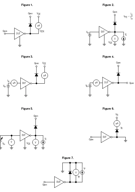
Output Leakage Current (Figure 1)
(VO = 50 V, TA = +70
°
C)
(VO = 50 V, TA = +25
°
C)
(VO = 50 V, TA = +70
°
C, VI = 6.0 V)
(VO = 50 V, TA = +70
°
C, VI = 1.0 V)
All Types
All Types
ULN2802
Collector–Emitter Saturation Voltage (Figure 2)
(IC = 350 mA, IB = 500
µ
A)
(IC = 200 mA, IB = 350
µ
A)
(IC = 100 mA, IB = 250
µ
A)
All Types
All Types
All Types
VCE(sat)
Input Current – On Condition (Figure 4)
(VI = 17 V)
Input Voltage – On Condition (Figure 5)
(VCE = 2.0 V, IC = 300 mA)
Input Current – Off Condition (Figure 3)
(IC = 500
µ
A, TA = +70
°
C)
All Types
II(off)
50
100
–
µ
A
DC Current Gain (Figure 2)
(VCE = 2.0 V, IC = 350 mA)
ULN2801
hFE
1000
–
–
–
Input Capacitance
CI
–
15
25
pF
Turn–On Delay Time
(50% EI to 50% EO)
ton
–
0.25
1.0
µ
s
Turn–Off Delay Time
(50% EI to 50% EO)
toff
–
0.25
1.0
µ
s
Clamp Diode Leakage Current (Figure 6)
(VR = 50 V)
Clamp Diode Forward Voltage (Figure 7)
(IF = 350 mA)
IC VCE
Open
µA
Open ICEX
DUT
V DUT
Open
Vin
VCE
V IC
µA
DUT
IR VR
DUT
Open
VCE
Open Vin V
TEST FIGURES
VCE Open
µA
DUT
µA Vin
Iin
hFE+IIC
in
(See Figure Numbers in Electrical Characteristics Table)
Open DUT
Open
Vin
µA
Figure 1.
Figure 2.
Figure 3.
Figure 4.
Figure 5.
Figure 6.
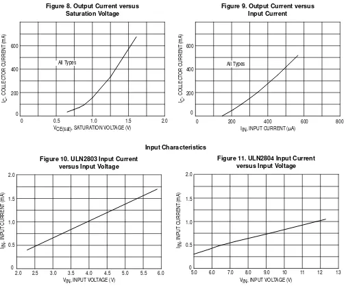
200
2.0
5.0
VIN, INPUT VOLTAGE (V)
12
All Types
IIN, INPUT CURRENT (
µ
A)
All Types
0
600
400
VCE(sat), SATURATION VOLTAGE (V)
1.5
VIN, INPUT VOLTAGE (V)
Input Characteristics
Figure 8. Output Current versus
Saturation Voltage
I , INPUT
CURRENT
(mA)
IN
I , INPUT
CURRENT
(mA)
TYPICAL CHARACTERISTIC CURVES – TA = 25
°
C, unless otherwise noted
Output Characteristics
Figure 9. Output Current versus
Input Current
Figure 10. ULN2803 Input Current
versus Input Voltage
Figure 11. ULN2804 Input Current
versus Input Voltage
13
2.7 k
7.2 k
3.0 k
Pin 10
1/8 ULN2803
3.0 k 7.2 k
10.5 k
1/8 ULN2804
Figure 12. Representative Schematic Diagrams
OUTLINE DIMENSIONS
NOTES:
1. POSITIONAL TOLERANCE OF LEADS (D), SHALL BE WITHIN 0.25 (0.010) AT MAXIMUM MATERIAL CONDITION, IN RELATION TO SEATING PLANE AND EACH OTHER. 2. DIMENSION L TO CENTER OF LEADS WHEN
FORMED PARALLEL.
3. DIMENSION B DOES NOT INCLUDE MOLD FLASH.
1
SEATING PLANE 10
9 18
M
A
B
K
C
N
F
G
D
H
J
L
DIM MIN MAX MIN MAXINCHES MILLIMETERS
A 22.22 23.24 0.875 0.915
B 6.10 6.60 0.240 0.260
C 3.56 4.57 0.140 0.180
D 0.36 0.56 0.014 0.022
F 1.27 1.78 0.050 0.070
G 2.54 BSC 0.100 BSC
H 1.02 1.52 0.040 0.060
J 0.20 0.30 0.008 0.012
K 2.92 3.43 0.115 0.135
L 7.62 BSC 0.300 BSC
M 0 15 0 15
N 0.51
_
1.02_
0.020_
0.040_
A SUFFIX
PLASTIC PACKAGE
CASE 707–02
Motorola reserves the right to make changes without further notice to any products herein. Motorola makes no warranty, representation or guarantee regarding the suitability of its products for any particular purpose, nor does Motorola assume any liability arising out of the application or use of any product or circuit, and specifically disclaims any and all liability, including without limitation consequential or incidental damages. “Typical” parameters which may be provided in Motorola data sheets and/or specifications can and do vary in different applications and actual performance may vary over time. All operating parameters, including “Typicals” must be validated for each customer application by customer’s technical experts. Motorola does not convey any license under its patent rights nor the rights of others. Motorola products are not designed, intended, or authorized for use as components in systems intended for surgical implant into the body, or other applications intended to support or sustain life, or for any other application in which the failure of the Motorola product could create a situation where personal injury or death may occur. Should Buyer purchase or use Motorola products for any such unintended or unauthorized application, Buyer shall indemnify and hold Motorola and its officers, employees, subsidiaries, affiliates, and distributors harmless against all claims, costs, damages, and expenses, and reasonable attorney fees arising out of, directly or indirectly, any claim of personal injury or death associated with such unintended or unauthorized use, even if such claim alleges that Motorola was negligent regarding the design or manufacture of the part. Motorola and are registered trademarks of Motorola, Inc. Motorola, Inc. is an Equal Opportunity/Affirmative Action Employer.
How to reach us:
USA / EUROPE / Locations Not Listed: Motorola Literature Distribution; JAPAN: Nippon Motorola Ltd.; Tatsumi–SPD–JLDC, 6F Seibu–Butsuryu–Center, P.O. Box 20912; Phoenix, Arizona 85036. 1–800–441–2447 or 602–303–5454 3–14–2 Tatsumi Koto–Ku, Tokyo 135, Japan. 03–81–3521–8315
MFAX: [email protected] – TOUCHTONE 602–244–6609 ASIA/PACIFIC: Motorola Semiconductors H.K. Ltd.; 8B Tai Ping Industrial Park,