1. Introduction
This document describes the functionality of the contactless reader/writer MFRC522. It includes the functional and electrical specifications.
2. General description
The MFRC522 is a highly integrated reader/writer for contactless communication at 13.56 MHz. The MFRC522 reader supports ISO 14443A / MIFARE® mode.
The MFRC522’s internal transmitter part is able to drive a reader/writer antenna designed to communicate with ISO/IEC 14443A/MIFARE® cards and transponders without
additional active circuitry. The receiver part provides a robust and efficient implementation of a demodulation and decoding circuitry for signals from ISO/IEC 14443A/MIFARE® compatible cards and transponders. The digital part handles the complete
ISO/IEC 14443A framing and error detection (Parity & CRC).The MFRC522 supports MIFARE®Classic (e.g. MIFARE® Standard) products. The MFRC522 supports contactless communication using MIFARE® higher transfer speeds up to 848 kbit/s in both directions.
Various host interfaces are implemented:
•
SPI interface•
serial UART (similar to RS232 with voltage levels according pad voltage supply)•
I2C interface.3. Features
Highly integrated analog circuitry to demodulate and decode responses
Buffered output drivers to connect an antenna with minimum number of external components
Supports ISO/IEC 14443A / MIFARE®
Typical operating distance in Reader/Writer mode for communication to a
ISO/IEC 14443A / MIFARE® up to 50 mm depending on the antenna size and tuning
Supports MIFARE® Classic encryption in Reader/Writer mode
Supports ISO/IEC 14443A higher transfer speed communication up to 848 kbit/s
Support of the MFIN / MFOUT
Additional power supply to directly supply the smart card IC connected via MFIN / MFOUT
Rev. 3.2 — 22 May 2007
Product data sheet
SPI interface up to 10 Mbit/s
I2C interface up to 400 kbit/s in Fast mode, up to 3400 kbit/s in High-speed mode
serial UART in different transfer speeds up to 1228.8 kbit/s, framing according to the RS232 interface with voltage levels according pad voltage supply
Comfortable 64 byte send and receive FIFO-buffer
Flexible interrupt modes
Hard reset with low power function
Power-down mode per software
Programmable timer
Internal oscillator to connect 27.12 MHz quartz
2.5 - 3.3 V power supply
CRC Co-processor
Free programmable I/O pins
4. Quick reference data
[1] Supply voltage below 3 V reduces the performance (e.g. the achievable operating distance).
[2] AVDD, DVDD and TVDD shall always be on the same voltage level.
[3] PVDD shall always be on the same or lower voltage level than DVDD.
[4] ITVDD depends on TVDD and the external circuitry connected to Tx1 and Tx2
[5] IPVDD depends on the overall load at the digital pins.
[6] During operation with a typical circuitry the overall current is below 100 mA.
[7] ISPD and IHPD are the total currents over all supplies.
[8] Typical value using a complementary driver configuration and an antenna matched to 40 Ω between TX1 and TX2 at 13.56 MHz
Table 1. Quick reference data
Symbol Parameter Conditions Min Typ Max Unit
AVDD Supply Voltage AVSS= DVSS= PVSS= TVSS= 0 V,
PVDD≤AVDD= DVDD=TVDD
[1][2] 2.5 - 3.6 V
DVDD [1][2]
TVDD [1][2]
PVDD Pad power supply AVSS= DVSS= PVSS= TVSS= 0 V,
PVDD≤AVDD= DVDD=TVDD
[3] 1.6 - 3.6 V
SVDD MFIN/MFOUT Pad Power
Supply
AVSS= DVSS= PVSS= TVSS= 0 V, 1.6 - 3.6 V
IHPD Hard Power-down Current AVDD= DVDD= TVDD= PVDD= 3 V,
NRESET= LOW
[4] - - 5 μA
ISPD Soft Power-down Current AVDD= DVDD= TVDD= PVDD= 3 V,
RF level detector on
[4] - - 10 μA
IDVDD Digital Supply Current DVDD= 3 V - 6.5 9 mA
IAVDD Analog Supply Current AVDD= 3 V, bit RCVOff = 0 - 7 10 mA
IAVDD,RCVOFF Analog Supply Current,
receiver switched off
AVDD= 3 V, bit RCVOff = 1 - 3 5 mA
IPVDD Pad Supply Current [2] - - 40 mA
ITVDD Transmitter Supply Current Continuous Wave [1][3][8] - 60 100 mA
5. Ordering information
Table 2: Ordering information
Type number Package
Name Description Version
MFRC52201HN1/TRAYB (delivered in 1 Tray)
HVQFN32 see Package Outline in Figure 33 “Package outline package version
(HVQFN32)”
see Packing Information in Figure 34 “Packing Information 1 Tray”
SOT617-1
MFRC52201HN1/TRAYBM (delivered in 5 Tray)
HVQFN32 see Package Outline in Figure 33 “Package outline package version
(HVQFN32)”
see Packing Information in Figure 35 “Packing Information 5Tray”
6. Block diagram
The Analog interface handles the modulation and demodulation of the analog signals.
The contactless UART handles the protocol requirements for the communication schemes in co-operation with the host. The comfortable FIFO buffer allows a fast and convenient data transfer from the host to the contactless UART and vice versa.
Various host interfaces are implemented to fulfil different customer requirements.
Fig 1. Simplified MFRC522 Block diagram
Contactless UART
FIFO
I2C Serial UART
SPI Registerbank
Host Analog
SPI, UART, I2C Interface Control
Control Register Bank 64 Byte FIFO
Serial Data Switch Parallel/Seriell Converter
Programable Timer
D1 to D7 EA, I2C
SDA
MIFARE Classic Unit
Bit Counter
Parity Generation & Check
Frame Generation & Check CRC16 Generation & Check
Power Down Control Command Register State Machine Reset Control DVDD DVSS NRSTPD
Bit Decoding Bit Coding
Transmitter Control TX1 TX2 TVSS TVDD FIFO Control Q-Clock Generation Oscillator OSCIN OSCOUT Q-Channel Amplifier Q-Channel Demodulator I-Channel Demodulator A/D Converter Amplitude Rating I-Channel Amplifier Reference Voltage VMID RX Analog Test MUX and DAC AUX1,2 Interrupt Control Voltage Monitor & Power On Detect IRQ Clock Generation, Filtering and Distribution V + G N D V + G N D PVDD PVSS
Random Number Generator
7. Pinning information
7.1 Pinning
7.2 Pin description
Fig 3. Pinning configuration HVQFN32 (SOT617-1).
Table 3: Pin description
Symbol Pin Type Description
I2C 1 I I2C enable[2]
PVDD 2 PWR Pad power supply
DVDD 3 PWR Digital Power Supply
DVSS 4 PWR Digital Ground[1]
PVSS 5 PWR Pad power supply ground
NRSTPD 6 I Not Reset and Power-down: When LOW, internal current
sinks are switched off, the oscillator is inhibited, and the input pads are disconnected from the outside world. With a positive edge on this pin the internal reset phase starts.
[1] Connection of heat sink pad on package buttom side is not necessary. Optional connection to DVSS is possible.
[2] The pin functionality for the interfaces is explained in Section 10 “DIGITAL Interfaces”.
TX1 11 O Transmitter 1: delivers the modulated 13.56 MHz energy carrier
TVDD 12 PWR Transmitter Power Supply: supplies the output stage of TX1 and TX2
TX2 13 O Transmitter 2: delivers the modulated 13.56 MHz energy carrier
TVSS 10, 14 PWR Transmitter Ground: supplies the output stage of TX1 and
TX2
AVDD 15 PWR Analog Power Supply
VMID 16 PWR Internal Reference Voltage: This pin delivers the internal reference voltage.
RX 17 I Receiver Input. Pin for the received RF signal. AVSS 18 PWR Analog Ground
AUX1 19 O Auxiliary Outputs: These pins are used for testing.
AUX2 20 O
OSCIN 21 I Crystal Oscillator Input: input to the inverting amplifier of the
oscillator. This pin is also the input for an externally generated clock (fosc= 27.12 MHz).
OSCOUT 22 O Crystal Oscillator Output: Output of the inverting amplifier of
the oscillator.
IRQ 23 O Interrupt Request: output to signal an interrupt event SDA 24 I Serial Data Line[2]
D1 25 I/O Data Pins for different interfaces (test port, I2IC, SPI,
UART)[2]
D2 26 I/O
D3 27 I/O
D4 28 I/O
D5 29 I/O
D6 30 I/O
D7 31 I/O
EA 32 I External Address: This Pin is used for coding I2C Address[2] Table 3: Pin description …continued
8. Functional description
MFRC522 transmission module supports the Reader/Writer mode for
ISO/IEC 14443A/MIFARE® with different transfer speeds and modulation schemes.
The following diagram Figure 5 “ISO/IEC 14443A/MIFARE® Reader/Writer mode
communication diagram.” describes the communication on a physical level.
The communication overview in Table 4 “Communication overview for ISO/IEC 14443A/MIFARE® reader/writer” describes the physical parameters.
Fig 4. MFRC522 Reader/Writer mode.
Fig 5. ISO/IEC 14443A/MIFARE® Reader/Writer mode communication diagram.
Table 4: Communication overview for ISO/IEC 14443A/MIFARE® reader/writer
Communication direction
ISO/IEC 14443A/ MIFARE®
transfer speed
106 kbit/s 212 kbit/s 424 kbit/s 848 kbit/s
Reader → Card
(send data from the MFRC522 to a
Modulation on reader side
100% ASK 100% ASK 100% ASK 100% ASK
ISO 14443A Card
RC522
Battery
µC
Reader/Writer
Contactless Card
ISO14443A
Reader ISO14443A
Card 1. Reader to Card 100 % ASK ,
Miller Coded,
Transfer speed 106 to 848 kbit/s
2. Card to Reader, Subcarrier Loadmodulation, Manchester Coded or BPSK,
RC522
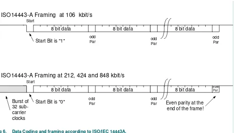
The contactless UART of MFRC522 and a dedicated external host are required to handle the complete MIFARE® / ISO/IEC 14443A / MIFARE® protocol. The following Figure 6
“Data Coding and framing according to ISO/IEC 14443A.” shows the Data Coding and framing according to ISO/IEC 14443A / MIFARE®.
The internal CRC co-processor calculates the CRC value according to the definitions given in the ISO/IEC 14443A part 3 and handles parity generation internally according to the transfer speed. Automatic parity generation can be switched off by bit ParityDisable in register 0x1D ManualRCVReg.
Card→Reader
(MFRC522 receives data from a card)
modulation on card side
subcarrier load modulation subcarrier load modulation subcarrier load modulation subcarrier load modulation subcarrier frequency
13.56 MHz/16 13.56MHz/16 13.56MHz/16 13.56MHz/16
bit coding Manchester
coding
BPSK BPSK BPSK
Table 4: Communication overview for ISO/IEC 14443A/MIFARE® reader/writer …continued
Communication direction
ISO/IEC 14443A/ MIFARE®
transfer speed
106 kbit/s 212 kbit/s 424 kbit/s 848 kbit/s
Fig 6. Data Coding and framing according to ISO/IEC 14443A.
Start
odd Par 8 bit data
odd Par 8 bit data
odd Par 8 bit data
Start Bit is "1"
ISO14443-A Framing at 106 kbit/s
Start
odd Par 8 bit data
odd Par
8 bit data 8 bit data evenPar.
Start Bit is "0" Burst of
32 sub-carrier clocks
Even parity at the end of the frame!
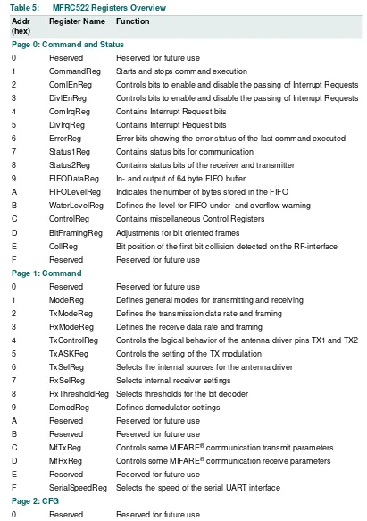
9. MFRC522 Register SET
9.1 MFRC522 Registers Overview
Table 5: MFRC522 Registers Overview
Addr (hex)
Register Name Function
Page 0: Command and Status
0 Reserved Reserved for future use
1 CommandReg Starts and stops command execution
2 ComlEnReg Controls bits to enable and disable the passing of Interrupt Requests
3 DivlEnReg Controls bits to enable and disable the passing of Interrupt Requests
4 ComIrqReg Contains Interrupt Request bits
5 DivIrqReg Contains Interrupt Request bits
6 ErrorReg Error bits showing the error status of the last command executed
7 Status1Reg Contains status bits for communication
8 Status2Reg Contains status bits of the receiver and transmitter
9 FIFODataReg In- and output of 64 byte FIFO buffer
A FIFOLevelReg Indicates the number of bytes stored in the FIFO
B WaterLevelReg Defines the level for FIFO under- and overflow warning
C ControlReg Contains miscellaneous Control Registers
D BitFramingReg Adjustments for bit oriented frames
E CollReg Bit position of the first bit collision detected on the RF-interface
F Reserved Reserved for future use
Page 1: Command
0 Reserved Reserved for future use
1 ModeReg Defines general modes for transmitting and receiving
2 TxModeReg Defines the transmission data rate and framing
3 RxModeReg Defines the receive data rate and framing
4 TxControlReg Controls the logical behavior of the antenna driver pins TX1 and TX2
5 TxASKReg Controls the setting of the TX modulation
6 TxSelReg Selects the internal sources for the antenna driver
7 RxSelReg Selects internal receiver settings
8 RxThresholdReg Selects thresholds for the bit decoder
9 DemodReg Defines demodulator settings
A Reserved Reserved for future use
B Reserved Reserved for future use
C MfTxReg Controls some MIFARE® communication transmit parameters
1 CRCResultReg Shows the actual MSB and LSB values of the CRC calculation
2
3 Reserved Reserved for future use
4 ModWidthReg Controls the setting of the ModWidth
5 Reserved Reserved for future use
6 RFCfgReg Configures the receiver gain
7 GsNReg Selects the conductance of the antenna driver pins TX1 and TX2 for
modulation
8 CWGsPReg
9 ModGsPReg
A TModeReg
TPrescalerReg
Defines settings for the internal timer
B
C TReloadReg Describes the 16 bit timer reload value
D
E TCounterValReg Shows the 16 bit actual timer value
F
Page 3: TestRegister
0 Reserved Reserved for future use
1 TestSel1Reg General test signal configuration
2 TestSel2Reg General test signal configuration and PRBS control
3 TestPinEnReg Enables pin output driver on D1-D7
4 TestPinValueReg Defines the values for D1 - D7 when it is used as I/O bus
5 TestBusReg Shows the status of the internal testbus
6 AutoTestReg Controls the digital selftest
7 VersionReg Shows the version
8 AnalogTestReg Controls the pins AUX1 and AUX2
9 TestDAC1Reg Defines the test value for the TestDAC1
A TestDAC2Reg Defines the test value for the TestDAC2
B TestADCReg Shows the actual value of ADC I and Q
C-F Reserved Reserved for production tests
Table 5: MFRC522 Registers Overview …continued
Addr (hex)
9.1.1 Register Bit Behavior
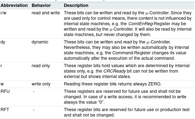
Depending on the functionality of a register, the access conditions to the register can vary. In principle bits with same behavior are grouped in common registers. In Table 6 the access conditions are described.
9.2 Register Description
9.2.1 Page 0: Command and Status
9.2.1.1 Reserved
Functionality is reserved for further use.
9.2.1.2 CommandReg
Starts and stops command execution.
Table 6: Behavior of Register Bits and its Designation
Abbreviation Behavior Description
r/w read and write These bits can be written and read by the μ-Controller. Since they
are used only for control means, there content is not influenced by
internal state machines, e.g. the ComIEnReg-Register may be
written and read by the μ-Controller. It will also be read by internal state machines, but never changed by them.
dy dynamic These bits can be written and read by the μ-Controller.
Nevertheless, they may also be written automatically by internal state machines, e.g. the Command-Register changes its value automatically after the execution of the actual command.
r read only These register bits hold values which are determined by internal
states only, e.g. the CRCReady bit can not be written from external but shows internal states.
w write only Reading these register bits returns always ZERO.
RFU - These registers are reserved for future use and shall not be
changed. In case of a write access, it is recommended to write always the value “0”.
RFT - These register bits are reserved for future use or production test
and shall not be changed.
Table 7: Reserved register (address 00h); reset value: 00h
Bit 7 6 5 4 3 2 1 0
Symbol
-Access Rights
RFU
Table 8: Description of Reserved register bits
Bit Symbol Description
9.2.1.3 CommIEnReg
Control bits to enable and disable the passing of interrupt requests. Table 9: CommandReg register (address 01h); reset value: 20h
Bit 7 6 5 4 3 2 1 0
Symbol - RcvOff Power Down Command
Access Rights
RFU r/w dy dy
Table 10: Description of CommandReg bits
Bit Symbol Description
7 to 6 - Reserved for future use.
5 RcvOff Set to logic 1, the analog part of the receiver is switched off.
4 PowerDown Set to logic 1, Soft Power-down mode is entered.
Set to logic 0, the MFRC522 starts the wake up procedure. During this procedure this bit still shows a logic 1. A logic 0 indicates that the
MFRC522 is ready for operations; see Section 16.2 “Soft
Power-down”.
Remark: The bit PowerDown cannot be set, when the command SoftReset has been activated.
3 to 0 Command Activates a command according to the Command Code. Reading this
register shows which command is actually executed (see Section 18.3
“MFRC522 Commands Overview”).
Table 11: CommIEnReg register (address 02h); reset value: 80h
Bit 7 6 5 4 3 2 1 0
Symbol IRqInv TxIEn RxIEn IdleIEn HiAlertIEn LoAlertIEn ErrIEn TimerIEn
Access Rights
r/w r/w r/w r/w r/w r/w r/w r/w
Table 12: Description of CommIEnReg bits
Bit Symbol Description
7 IRqInv Set to logic 1, the signal on pin IRQ is inverted with respect to bit IRq in the
register Status1Reg.
Set to logic 0, the signal on pin IRQ is equal to bit IRq. In combination with bit IRqPushPull in register DivIEnReg, the default value of logic 1 ensures, that the output level on pin IRQ is tristate.
6 TxIEn Allows the transmitter interrupt request (indicated by bit TxIRq) to be
propagated to pin IRQ.
5 RxIEn Allows the receiver interrupt request (indicated by bit RxIRq) to be
propagated to pin IRQ.
4 IdleIEn Allows the idle interrupt request (indicated by bit IdleIRq) to be propagated to
pin IRQ.
3 HiAlertIEn Allows the high alert interrupt request (indicated by bit HiAlertIRq) to be
2 LoAlertIEn Allows the low alert interrupt request (indicated by bit LoAlertIRq) to be propagated to pin IRQ.
1 ErrIEn Allows the error interrupt request (indicated by bit ErrIRq) to be propagated
to pin IRQ.
0 TimerIEn Allows the timer interrupt request (indicated by bit TimerIRq) to be
propagated to pin IRQ.
Table 12: Description of CommIEnReg bits
9.2.1.4 DivIEnReg
Control bits to enable and disable the passing of interrupt requests.
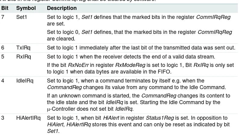
9.2.1.5 CommIRqReg
Contains Interrupt Request bits.
Table 13: DivIEnReg register (address 03h); reset value: 00h
Bit 7 6 5 4 3 2 1 0
Symbol IRQPushPull - MfinActIEn - CRCIEn
-Access Rights
r/w RFU r/w RFU r/w RFU
Table 14: Description of DivIEnReg bits
Bit Symbol Description
7 IRQPushPull Set to logic 1, the pin IRQ works as standard CMOS output pad.
Set to logic 0, the pin IRQ works as open drain output pad.
6 to 5 - Reserved for future use.
4 MfinActIEn Allows the MFIN active interrupt request to be propagated to pin IRQ.
3 - Reserved for future use.
2 CRCIEn Allows the CRC interrupt request (indicated by bit CRCIRq) to be
propagated to pin IRQ.
1 to 0 - Reserved for future use.
Table 15: CommIRqReg register (address 04h); reset value: 14h
Bit 7 6 5 4 3 2 1 0
Symbol Set1 TxIRq RxIRq IdleIRq HiAlertIRq LoAlertIRq ErrIRq TimerIRq
Access Rights
w dy dy dy dy dy dy dy
Table 16: Description of CommIRqReg bits
All bits in the register CommIRqReg shall be cleared by software.
Bit Symbol Description
7 Set1 Set to logic 1, Set1 defines that the marked bits in the register CommIRqReg
are set.
Set to logic 0, Set1 defines, that the marked bits in the register CommIRqReg
are cleared.
6 TxIRq Set to logic 1 immediately after the last bit of the transmitted data was sent out.
5 RxIRq Set to logic 1 when the receiver detects the end of a valid data stream.
If the bit RxNoErr in register RxModeReg is set to logic 1, Bit RxIRq is only set to logic 1 when data bytes are available in the FIFO.
4 IdleIRq Set to logic 1, when a command terminates by itself e.g. when the
CommandReg changes its value from any command to the Idle Command.
If an unknown command is started, the CommandReg changes its content to
the idle state and the bit IdleIRq is set. Starting the Idle Command by the
μ-Controller does not set bit IdleIRq.
9.2.1.6 DivIRqReg
Contains Interrupt Request bits
2 LoAlertIRq Set to logic 1, when bit LoAlert in register Status1Reg is set. In opposition to
LoAlert, LoAlertIRq stores this event and can only be reset as indicated by bit
Set1.
1 ErrIRq Set to logic 1 if any error bit in the ErrorReg Register is set.
0 TimerIRq Set to logic 1 when the timer decrements the TimerValue Register to zero.
Table 16: Description of CommIRqReg bits …continued
All bits in the register CommIRqReg shall be cleared by software.
Bit Symbol Description
Table 17: DivIRqReg register (address 05h); reset value: X0h
Bit 7 6 5 4 3 2 1 0
Symbol Set2 - MfinActIRq - CRCIRq
-Access Rights
w RFU dy RFU dy RFU
Table 18: Description of DivIRqReg bits
All bits in the register DivIRqReg shall be cleared by software.
Bit Symbol Description
7 Set2 Set to logic 1, Set2 defines that the marked bits in the register
DivIRqReg are set.
Set to logic 0, Set2 defines, that the marked bits in the register
DivIRqReg are cleared
6 to 5 - Reserved for future use.
4 MfinActIRq Set to logic 1, when MFIN is active. This interrupt is set when either a
rising or falling signal edge is detected.
3 - Reserved for future use.
2 CRCIRq Set to logic 1, when the CRC command is active and all data are
processed.
9.2.1.7 ErrorReg
Error bit register showing the error status of the last command executed.
[1] Command execution will clear all error bits except for bit TempErr. A setting by software is impossible.
Table 19: ErrorReg register (address 06h); reset value: 00h
Bit 7 6 5 4 3 2 1 0
Symbol WrErr TempErr - BufferOvfl CollErr CRCErr ParityErr ProtocolErr
Access Rights
r r RFU r r r r r
Table 20: Description of ErrorReg bits
Bit Symbol Description
7 WrErr Set to logic 1, when data is written into the FIFO by the host during the
MFAuthent command or if data is written into the FIFO by the host during the time between sending the last bit on the RF interface and receiving the last bit on the RF interface.
6 TempErr[1] Set to logic 1, if the internal temperature sensor detects overheating.
In this case, the antenna drivers are switched off automatically.
5 - Reserved for future use.
4 BufferOvfl Set to logic 1, if the host or a MFRC522’s internal state machine (e.g.
receiver) tries to write data into the FIFO buffer although the FIFO buffer is already full.
3 CollErr Set to logic 1, if a bit-collision is detected. It is cleared automatically at
receiver start-up phase. This bit is only valid during the bitwise anticollision at 106 kbit/s. During communication schemes at 212, 424 and 848 kbit/s this bit is always set to logic 0.
2 CRCErr Set to logic 1, if bit RxCRCEn in register RxModeReg is set and the
CRC calculation fails. It is cleared to logic 0 automatically at receiver start-up phase.
1 ParityErr Set to logic 1, if the parity check has failed. It is cleared automatically
at receiver start-up phase. Only valid for ISO/IEC 14443A/MIFARE®
communication at 106 kbit/s.
0 ProtocolErr Set to logic 1, if one out of the following cases occur:
•
Set to logic 1 if the SOF is incorrect. It is cleared automatically at receiver start-up phase. The bit is only valid for 106 kbit/s.9.2.1.8 Status1Reg
Contains status bits of the CRC, Interrupt and FIFO buffer.
Table 21: Status1Reg register (address 07h); reset value: 21h
Bit 7 6 5 4 3 2 1 0
Symbol - CRCOk CRCReady IRq TRunning - HiAlert LoAlert
Access Rights
RFU r r r r RFU r r
Table 22: Description of Status1Reg bits
Bit Symbol Description
7 - Reserved for future use.
6 CRCOk Set to logic 1, if the CRC result is zero. For data transmission and
reception the bit CRCOk is undefined (use CRCErr in register
ErrorReg). CRCOk indicates the status of the CRC co-processor, during calculation the value changes to logic 0, when the calculation is done correctly, the value changes to logic 1.
5 CRCReady Set to logic 1, when the CRC calculation has finished. This bit is only
valid for the CRC co-processor calculation using the command CalcCRC.
4 IRq This bit shows, if any interrupt source requests attention (with respect
to the setting of the interrupt enable bits, see register CommIEnReg
and DivIEnReg).
3 TRunning Set to logic 1, if the MFRC522’s timer unit is running, e.g. the timer will
decrement the TCounterValReg with the next timer clock.
Remark: In the gated mode the bit TRunning is set to logic 1, when the timer is enabled by the register bits. This bit is not influenced by the gated signal.
2 - Reserved for future use.
1 HiAlert Set to logic 1, when the number of bytes stored in the FIFO buffer
fulfils the following equation:
Example:
FIFOLength = 60, WaterLevel = 4→HiAlert = 1
FIFOLength = 59, WaterLevel = 4→HiAlert = 0
0 LoAlert Set to logic 1, when the number of bytes stored in the FIFO buffer
fulfils the following equation:
Example:
FIFOLength = 4, WaterLevel = 4→LoAlert = 1
FIFOLength = 5, WaterLevel = 4→LoAlert = 0
HiAlert = (64–FIFOLength)≤WaterLevel
9.2.1.9 Status2Reg
Contains status bits of the receiver, transmitter and data mode detector.
Table 23: Status2Reg register (address 08h); reset value: 00h
Bit 7 6 5 4 3 2 1 0
Symbol TempSens
Clear
I2CForceHS - MFCrypto1On Modem State
Access Rights
r/w r/w RFU dy r
Table 24: Description of Status2Reg bits
Bit Symbol Description
7 TempSensClear Set to logic 1, this bit clears the temperature error, if the temperature
is below the alarm limit of 125°C.
6 I2CForceHS I2C input filter settings.
Set to logic 1, the I2C input filter is set to the High-speed mode
independent of the I2C protocol.
Set to logic 0, the I2C input filter is set to the used I2C protocol.
5 to 4 - Reserved for future use.
3 MFCrypto1On This bit indicates that the MIFARE® Crypto1 unit is switched on and
therefore all data communication with the card is encrypted. This bit can only be set to logic 1 by a successful execution of the MFAuthent Command. This bit is only valid in Reader/Writer mode for MIFARE® Standard cards. This bit shall be cleared by software.
2 to 0 Modem State ModemState shows the state of the transmitter and receiver state
machines. Status Description
000 IDLE
001 Wait for bit StartSend in register BitFramingReg
010 TxWait: Wait until Rf field is present, if the bit TxWaitRF is set to logic 1. The minimum time for TxWait is defined by the
TxWaitReg register.
011 Transmitting
100 RxWait: Wait until RF field is present, if the bit RxWaitRF is set to logic 1. The minimum time for RxWait is defined by the
RxWaitReg register.
101 Wait for data
9.2.1.10 FIFODataReg
In- and output of 64 byte FIFO buffer.
9.2.1.11 FIFOLevelReg
Indicates the number of bytes stored in the FIFO.
9.2.1.12 WaterLevelReg
Defines the level for FIFO under- and overflow warning. Table 25: FIFODataReg register (address 09h); reset value: XXh
Bit 7 6 5 4 3 2 1 0
Symbol FIFOData
Access Rights
dy
Table 26: Description ofFIFODataReg bits
Bit Symbol Description
7 to 0 FIFOData Data input and output port for the internal 64 byte FIFO buffer. The
FIFO buffer acts as parallel in/parallel out converter for all serial data stream in- and outputs.
Table 27: FIFOLevelReg register (address 0Ah); reset value: 00h
Bit 7 6 5 4 3 2 1 0
Symbol FlushBuffer FIFOLevel
Access Rights
w r
Table 28: Description of FIFOLevelReg bits
Bit Symbol Description
7 FlushBuffer Set to logic 1, this bit clears the internal FIFO-buffer’s read- and
write-pointer and the bit BufferOvfl in the register ErrReg immediately. Reading this bit will always return 0.
6 to 0 FIFOLevel Indicates the number of bytes stored in the FIFO buffer. Writing to the
FIFODataReg increments, reading decrements the FIFOLevel.
Table 29: WaterLevelReg register (address 0Bh); reset value: 08h
Bit 7 6 5 4 3 2 1 0
Symbol - WaterLevel
Access Rights
9.2.1.13 ControlReg
Miscellaneous control bits.
Table 30: Description of WaterLevelReg bits
Bit Symbol Description
7 to 6 - Reserved for future use.
5 to 0 WaterLevel This register defines a warning level to indicate a FIFO-buffer over- or
underflow:
The bit HiAlert in Status1Reg is set to logic 1, if the remaining number of bytes in the FIFO-buffer space is equal or less than the defined number of WaterLevel bytes.
The bit LoAlert in Status1Reg is set to logic 1, if equal or less than
WaterLevel bytes are in the FIFO.
Remark: For the calculation of HiAlert and LoAlert see Section 9.2.1.8 “Status1Reg”.
Table 31: ControlReg register (address 0Ch); reset value: 10h
Bit 7 6 5 4 3 2 1 0
Symbol TStopNow TStartNow - RxLastBits
Access Rights
w w RFU r
Table 32: Description of ControlReg bits
Bit Symbol Description
7 TStopNow Set to logic 1, the timer stops immediately.
Reading this bit will always return 0.
6 TStartNow Set to logic 1 starts the timer immediately.
Reading this bit will always return 0.
5 to 3 - Reserved for future use.
2 to 0 RxLastBits Shows the number of valid bits in the last received byte. If 0, the
9.2.1.14 BitFramingReg
Adjustments for bit oriented frames.
9.2.1.15 CollReg
Defines the first bit collision detected on the RF interface. Table 33: BitFramingReg register (address 0Dh); reset value: 00h
Bit 7 6 5 4 3 2 1 0
Symbol StartSend RxAlign - TxLastBits
Access Rights
w r/w RFU r/w
Table 34: Description of BitFramingReg bits
Bit Symbol Description
7 StartSend Set to logic 1, the transmission of data starts.
This bit is only valid in combination with the Transceive command.
6 to 4 RxAlign Used for reception of bit oriented frames: RxAlign defines the bit position
for the first bit received to be stored in the FIFO. Further received bits are stored at the following bit positions.
Example:
RxAlign = 0: the LSB of the received bit is stored at bit 0, the second received bit is stored at bit position 1.
RxAlign = 1: the LSB of the received bit is stored at bit 1, the second received bit is stored at bit position 2.
RxAlign = 7: the LSB of the received bit is stored at bit 7, the second received bit is stored in the following byte at bit position 0.
This bits shall only be used for bitwise anticollision at 106 kbit/s. In all other modes it shall be set to 0.
3 - Reserved for future use.
2 to 0 TxLastBits Used for transmission of bit oriented frames: TxLastBits defines the
number of bits of the last byte that shall be transmitted. A 000b indicates that all bits of the last byte shall be transmitted.
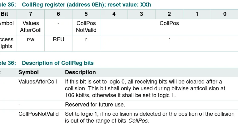
Table 35: CollReg register (address 0Eh); reset value: XXh
Bit 7 6 5 4 3 2 1 0
Symbol Values
AfterColl
- CollPos
NotValid
CollPos
Access Rights
r/w RFU r r
Table 36: Description of CollReg bits
Bit Symbol Description
7 ValuesAfterColl If this bit is set to logic 0, all receiving bits will be cleared after a
9.2.1.16 Reserved
Functionality is reserved for further use.
9.2.2 Page 1: Communication
9.2.2.1 Reserved
Functionality is reserved for further use.
4 to 0 CollPos These bits show the bit position of the first detected collision in a
received frame. Only data bits are interpreted.
Example:
00h indicates a bit collision in the 32nd bit
01h indicates a bit collision in the 1stbit
08h indicates a bit collision in the 8thbit
These bits shall only be interpreted if bit CollPosNotValid is set to logic 0.
Table 36: Description of CollReg bits
Bit Symbol Description
Table 37: Reserved register (address 0Fh); reset value: 00h
Bit 7 6 5 4 3 2 1 0
Symbol
-Access Rights
RFU
Table 38: Description of Reserved register bits
Bit Symbol Description
7 to 0 - Reserved for future use.
Table 39: Reserved register (address 10h); reset value: 00h
Bit 7 6 5 4 3 2 1 0
Symbol
-Access Rights
RFU
Table 40: Description of Reserved register bits
Bit Symbol Description
9.2.2.2 ModeReg
Defines general mode settings for transmitting and receiving.
9.2.2.3 TxModeReg
Defines the data rate during transmission.
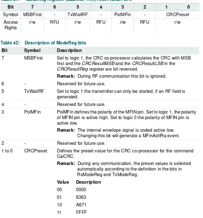
Table 41: ModeReg register (address 11h); reset value: 3Fh
Bit 7 6 5 4 3 2 1 0
Symbol MSBFirst - TxWaitRF - PolMFin - CRCPreset
Access Rights
r/w RFU r/w RFU r/w RFU r/w
Table 42: Description of ModeReg bits
Bit Symbol Description
7 MSBFirst Set to logic 1, the CRC co-processor calculates the CRC with MSB
first and the CRCResultMSB and the CRCResultLSB in the
CRCResultReg register are bit reversed.
Remark: During RF communication this bit is ignored.
6 - Reserved for future use.
5 TxWaitRF Set to logic 1 the transmitter can only be started, if an RF field is
generated.
4 - Reserved for future use.
3 PolMFin PolMFin defines the polarity of the MFIN pin. Set to logic 1, the polarity
of MFIN pin is active high. Set to logic 0 the polarity of MFIN pin is active low.
Remark: The internal envelope signal is coded active low. Changing this bit will generate a MFinActIRq event.
2 - Reserved for future use.
1 to 0 CRCPreset Defines the preset value for the CRC co-processor for the command
CalCRC.
Remark: During any communication, the preset values is selected automatically according to the definition in the bits in RxModeReg and TxModeReg.
Value Description
00 0000
01 6363
10 A671
11 FFFF
Table 43: TxModeReg register (address 12h); reset value: 00h
Bit 7 6 5 4 3 2 1 0
Symbol TxCRCEn TxSpeed InvMod
9.2.2.4 RxModeReg
Defines the data rate during reception. Table 44: Description of TxModeReg bits
Bit Symbol Description
7 TxCRCEn Set to logic 1, this bit enables the CRC generation during data
transmission.
Remark: This bit shall only be set to logic 0 at 106 kbit/s.
6 to 4 TxSpeed Defines the bit rate while data transmission. The MFRC522 handels
transfer speeds up to 848 kbit/s.
Value Description
000 106 kbit/s
001 212 kbit/s
010 424 kbit/s
011 848 kbit/s
100 Reserved
101 Reserved
110 Reserved
111 Reserved
3 InvMod Set to logic 1, the modulation for transmitting data is inverted.
2 to 0 - Reserved for future use.
Table 45: RxModeReg register (address 13h); reset value: 00h
Bit 7 6 5 4 3 2 1 0
Symbol RxCRCEn RxSpeed RxNoErr RxMultiple
-Access Rights
r/w dy r/w r/w RFU
Table 46: Description of RxModeReg bits
Bit Symbol Description
7 RxCRCEn Set to logic 1, this bit enables the CRC calculation during reception.
Remark: This bit shall only be set to logic 0 at 106 kbit/s.
6 to 4 RxSpeed Defines the bit rate while data receiving. The MFRC522 handles
transfer speeds up to 848kbit/s.
Value Description
000 106 kbit/s
001 212 kbit/s
010 424 kbit/s
011 848 kbit/s
100 Reserved
101 Reserved
110 Reserved
9.2.2.5 TxControlReg
Controls the logical behavior of the antenna driver pins Tx1 and Tx2.
3 RxNoErr If set to logic 1, a not valid received data stream (less than 4 bits
received) will be ignored. The receiver will remain active.
2 RxMultiple Set to logic 0, the receiver is deactivated after receiving a data frame.
Set to logic 1, it is possible to receive more than one data frame. This bit is only valid for data rates above 106 kbit/s to handle the Polling command. Having set this bit, the receive and transceive commands will not terminate automatically. In this case the multiple receiving can only be deactivated by writing any command (except the Receive command) to the CommandReg register or by clearing the bit by the host.
If set to logic 1, at the end of a received data stream an error byte is added to the FIFO. The error byte is a copy of the ErrorReg register.
1 to 0 - Reserved for future use.
Table 46: Description of RxModeReg bits …continued
Bit Symbol Description
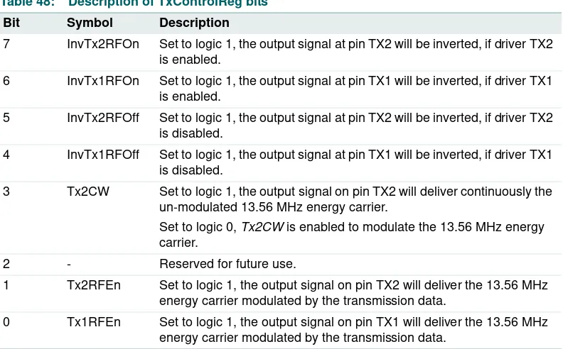
Table 47: TxControlReg register (address 14h); reset value: 80h
Bit 7 6 5 4 3 2 1 0
Symbol InvTx2RF
On
InvTx1RF On
InvTx2RF Off
InvTx1RF Off
Tx2CW - Tx2RFEn Tx1RFEn
Access Rights
r/w r/w r/w r/w r/w RFU r/w r/w
Table 48: Description of TxControlReg bits
Bit Symbol Description
7 InvTx2RFOn Set to logic 1, the output signal at pin TX2 will be inverted, if driver TX2
is enabled.
6 InvTx1RFOn Set to logic 1, the output signal at pin TX1 will be inverted, if driver TX1
is enabled.
5 InvTx2RFOff Set to logic 1, the output signal at pin TX2 will be inverted, if driver TX2
is disabled.
4 InvTx1RFOff Set to logic 1, the output signal at pin TX1 will be inverted, if driver TX1
is disabled.
3 Tx2CW Set to logic 1, the output signal on pin TX2 will deliver continuously the
un-modulated 13.56 MHz energy carrier.
Set to logic 0, Tx2CW is enabled to modulate the 13.56 MHz energy
carrier.
2 - Reserved for future use.
1 Tx2RFEn Set to logic 1, the output signal on pin TX2 will deliver the 13.56 MHz
energy carrier modulated by the transmission data.
0 Tx1RFEn Set to logic 1, the output signal on pin TX1 will deliver the 13.56 MHz
9.2.2.6 TxASKReg
Controls the settings of the transmit modulation.
9.2.2.7 TxSelReg
Selects the internal sources for the analog part.
Table 49: TxAutoReg register (address 15h); reset value: 00h
Bit 7 6 5 4 3 2 1 0
Symbol - Force100ASK
-Access Rights
RFU r/w RFU
Table 50: Description of TxAutoReg bits
Bit Symbol Description
7 - Reserved for future use.
6 Force100ASK Set to logic 1, Force100ASK forces a 100% ASK modulation
independent of the setting in register ModGsPReg.
5 to 0 - Reserved for future use.
Table 51: TxSelReg register (address 16h); reset value: 10h
Bit 7 6 5 4 3 2 1 0
Symbol - DriverSel MfOutSel
Access Rights
RFU r/w r/w
Table 52: Description of TxSelReg bits
Bit Symbol Description
7 to 6 - Reserved for future use.
5 to 4 DriverSel Selects the input of driver Tx1 and Tx2.
Value Description
00 Tristate
Remark: In soft power-down the drivers are only in tristate mode if DriverSel is set to tristate mode.
01 Modulation signal (envelope) from the internal coder, Miller
Pulse Coded.
10 Modulation signal (envelope) from MIFIN
11 High
9.2.2.8 RxSelReg
Selects internal receiver settings.
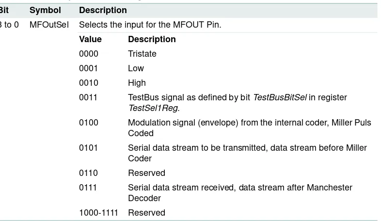
3 to 0 MFOutSel Selects the input for the MFOUT Pin.
Value Description
0000 Tristate
0001 Low
0010 High
0011 TestBus signal as defined by bit TestBusBitSel in register
TestSel1Reg.
0100 Modulation signal (envelope) from the internal coder, Miller Puls
Coded
0101 Serial data stream to be transmitted, data stream before Miller
Coder
0110 Reserved
0111 Serial data stream received, data stream after Manchester
Decoder
1000-1111 Reserved
Table 52: Description of TxSelReg bits
Bit Symbol Description
Table 53: RxSelReg register (address 17h); reset value: 84h
Bit 7 6 5 4 3 2 1 0
Symbol UartSel RxWait
Access Rights
r/w r/w
Table 54: Description of RxSelReg bits
Bit Symbol Description
7 to 6 UartSel Selects the input of the contactless UART
Value Description
00 Constant Low
01 Manchester with sub-carrier from MFIN pin
10 Modulation signal from the internal analog part, default
11 NRZ coding without sub-carrier from MFIN pin. Only valid for
transfer speeds above 106 kbit/s.
5 to 0 RxWait After data transmission, the activation of the receiver is delayed for
RxWait bit-clocks. During this ‘frame guard time’ any signal at pin Rx is ignored.This parameter is ignored by the receive command.
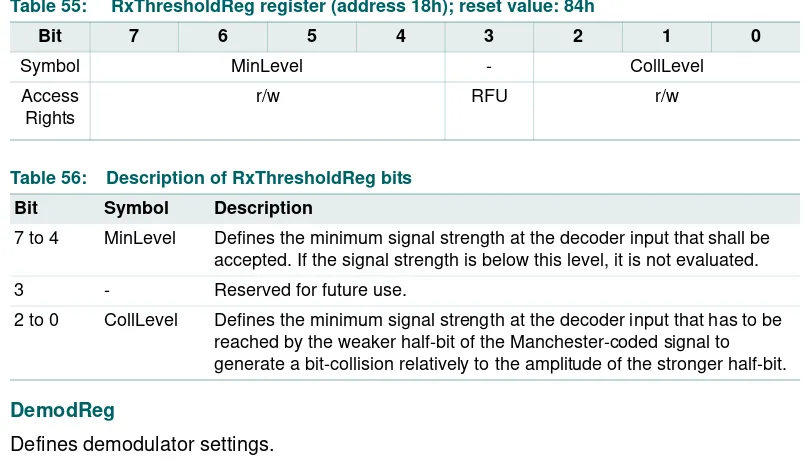
9.2.2.9 RxThresholdReg
Selects thresholds for the bit decoder.
9.2.2.10 DemodReg
Defines demodulator settings.
Table 55: RxThresholdReg register (address 18h); reset value: 84h
Bit 7 6 5 4 3 2 1 0
Symbol MinLevel - CollLevel
Access Rights
r/w RFU r/w
Table 56: Description of RxThresholdReg bits
Bit Symbol Description
7 to 4 MinLevel Defines the minimum signal strength at the decoder input that shall be
accepted. If the signal strength is below this level, it is not evaluated.
3 - Reserved for future use.
2 to 0 CollLevel Defines the minimum signal strength at the decoder input that has to be
reached by the weaker half-bit of the Manchester-coded signal to generate a bit-collision relatively to the amplitude of the stronger half-bit.
Table 57: DemodReg register (address 19h); reset value: 4Dh
Bit 7 6 5 4 3 2 1 0
Symbol AddIQ FixIQ - TauRcv TauSync
Access Rights
r/w r/w RFU r/w r/w
Table 58: Description of DemodReg bits
Bit Symbol Description
7 to 6 AddIQ Defines the use of I and Q channel during reception
Remark: FixIQ has to be set to logic 0 to enable the following settings.
Value Description
00 Select the stronger channel
01 Select the stronger channel and freeze the selected during
communication
10 Reserved
11 Reserved
5 FixIQ If set to logic 1 and the bits AddIQ are set to X0b, the reception is fixed to
I channel.
If set to logic 1 and the bits AddIQ are set to X1b, the reception is fixed to Q channel.
4 - Reserved for future use.
3 to 2 TauRcv Changes the time constant of the internal PLL during data reception.
Remark: If set to 00b, the PLL is frozen during data reception.
9.2.2.11 Reserved
Functionality is reserved for further use.
9.2.2.12 Reserved
Functionality is reserved for further use.
9.2.2.13 MfTxReg
Controls some MIFARE® communication transmit parameters
Table 59: Reserved register (address 1Ah); reset value: 00h
Bit 7 6 5 4 3 2 1 0
Symbol
-Access Rights
RFU
Table 60: Description of Reserved register bits
Bit Symbol Description
7 to 0 - Reserved for future use.
Table 61: Reserved register (address 1Bh); reset value: 00h
Bit 7 6 5 4 3 2 1 0
Symbol
-Access Rights
RFU
Table 62: Description of Reserved register bits
Bit Symbol Description
7 to 0 - Reserved for future use.
Table 63: MfTxReg register (address 1Ch); reset value: 62h
Bit 7 6 5 4 3 2 1 0
Symbol - TxWait
Access Rights
RFU r/w
Table 64: Description of MifNFCReg bits
Bit Symbol Description
7 to 2 - Reserved for future use.
1 to 0 TxWait These bits define the additional response time. Per default 7 bits are
9.2.2.14 MfRxReg
9.2.2.15 Reserved
Functionality is reserved for further use.
9.2.2.16 SerialSpeedReg
Selects the speed of the serial UART interface.
Table 65: MfRxReg register (address 1Dh); reset value: 00h
Bit 7 6 5 4 3 2 1 0
Symbol - Parity Disable
-Access Rights
RFU r/w RFU
Table 66: Description of ManualRCVReg bits
Bit Symbol Description
7 to 5 - Reserved for future use.
4 Parity Disable If this bit is set to logic 1, the generation of the Parity bit for
transmission and the Parity-Check for receiving is switched off. The received Parity bit is handled like a data bit.
3 to 0 - Reserved for future use.
Table 67: Reserved register (address 1Eh); reset value: 00h
Bit 7 6 5 4 3 2 1 0
Symbol
-Access Rights
RFU
Table 68: Description of Reserved register bits
Bit Symbol Description
7 to 0 - Reserved for future use.
Table 69: SerialSpeedReg register (address 1Fh); reset value: EBh
Bit 7 6 5 4 3 2 1 0
Symbol BR_T0 BR_T1
Access Rights
r/w r/w
Table 70: Description of SerialSpeedReg bits
Bit Symbol Description
7 to 5 BR_T0 Factor BR_T0 to adjust the transfer speed, for description see Section
10.3.2 “Selection of the transfer speeds”.
4 to 0 BR_T1 Factor BR_T1 to adjust the transfer speed, for description see Section
9.2.3 Page 2: Configuration
9.2.3.1 Reserved
Functionality is reserved for further use.
9.2.3.2 CRCResultReg
Shows the actual MSB and LSB values of the CRC calculation.
Remark: The CRC is split into two 8-bit register.
Table 71: Reserved register (address 20h); reset value: 00h
Bit 7 6 5 4 3 2 1 0
Symbol
-Access Rights
RFU
Table 72: Description of Reserved register bits
Bit Symbol Description
7 to 0 - Reserved for future use.
Table 73: CRCResultReg register (address 21h); reset value: FFh
Bit 7 6 5 4 3 2 1 0
Symbol CRCResultMSB
Access Rights
r
Table 74: Description of CRCResultReg higher bits
Bit Symbol Description
7 to 0 CRCResultMSB This register shows the actual value of the most significant byte of
the CRCResultReg register. It is valid only if bit CRCReady in register Status1Reg is set to logic 1.
Table 75: CRCResultReg register (address 22h); reset value: FFh
Bit 7 6 5 4 3 2 1 0
Symbol CRCResultLSB
Access Rights
r
Table 76: Description of CRCResultReg lower bits
Bit Symbol Description
7 to 0 CRCResultLSB This register shows the actual value of the least significant byte of
the CRCResult register. It is valid only if bit CRCReady in register
9.2.3.3 Reserved
Functionality is reserved for further use.
9.2.3.4 ModWidthReg
Controls the setting of modulation width.
9.2.3.5 Reserved
Functionality is reserved for further use.
Table 77: Reserved register (address 23h); reset value: 88h
Bit 7 6 5 4 3 2 1 0
Symbol
-Access Rights
RFU
Table 78: Description of Reserved register bits
Bit Symbol Description
7 to 0 - Reserved for future use.
Table 79: ModWidthReg register (address 24h); reset value: 26h
Bit 7 6 5 4 3 2 1 0
Symbol ModWidth
Access Rights
r/w
Table 80: Description of ModWidthReg bits
Bit Symbol Description
7 to 0 ModWidth These bits define the width of the Miller modulation as multiples of the
carrier frequency (ModWidth +1/fc). The maximum value is half the bit period.
Table 81: Reserved register (address 25h); reset value: 87h
Bit 7 6 5 4 3 2 1 0
Symbol
-Access Rights
RFU
Table 82: Description of Reserved register bits
Bit Symbol Description
9.2.3.6 RFCfgReg
Configures the receiver gain.
9.2.3.7 GsNReg
Selects the conductance for the N-driver of the antenna driver pins TX1 and TX2 when the driver is switched on.
Table 83: RFCfgReg register (address 26h); reset value: 48h
Bit 7 6 5 4 3 2 1 0
Symbol - RxGain
-Access Rights
RFU r/w RFU
Table 84: Description of RFCfgReg bits
Bit Symbol Description
7 - Reserved for future use.
6 to 4 RxGain This register defines the receivers signal voltage gain factor:
Value Description
000 18 dB
001 23 dB
010 18 dB
011 23 dB
100 33 dB
101 38 dB
110 43 dB
111 48 dB
3 to 0 - .Reserved for future use.
Table 85: GsNReg register (address 27h); reset value: 88h
Bit 7 6 5 4 3 2 1 0
Symbol CWGsN ModGsN
Access Rights
r/w r/w
Table 86: Description of GsNOnReg bits
Bit Symbol Description
7 to 4 CWGsN The value of this register defines the conductance of the output N-driver
during times of no modulation. This may be used to regulate the output power and subsequently current consumption and operating distance.
Remark: The conductance value is binary weighted.
9.2.3.8 CWGsPReg
Defines the conductance of the P-driver during times of no modulation
9.2.3.9 ModGsPReg
Defines the driver P-output conductance during modulation. Table 87: CWGsPReg register (address 28h); reset value: 20h
Bit 7 6 5 4 3 2 1 0
Symbol - CWGsP
Access Rights
RFU r/w
Table 88: Description of CWGsPReg bits
Bit Symbol Description
7 to 6 - Reserved for future use.
5 to 0 CWGsP The value of this register defines the conductance of the output
P-driver. This may be used to regulate the output power and subsequently current consumption and operating distance.
Remark: The conductance value is binary weighted.
During soft Power-down mode the highest bit is forced to 1.
Table 89: ModGsPReg register (address 29h); reset value: 20h
Bit 7 6 5 4 3 2 1 0
Symbol - ModGsP
Access Rights
RFU r/w
Table 90: Description of ModGsPReg bits
Bit Symbol Description
7 to 6 - Reserved for future use.
5 to 0 ModGsP The value of this register defines the conductance of the output
P-driver for the time of modulation. This may be used to regulate the modulation index.
Remark: The conductance value is binary weighted.
9.2.3.10 TMode Register, TPrescaler Register
Defines settings for the timer.
Remark: The Prescaler value is split over two registers.
Table 91: TModeReg register (address 2Ah); reset value: 00h
Bit 7 6 5 4 3 2 1 0
Symbol TAuto TGated TAutoRestart TPrescaler_Hi
Access Rights
r/w r/w r/w r/w
Table 92: Description of TModeReg bits
Bit Symbol Description
7 TAuto Set to logic 1, the timer starts automatically at the end of the
transmission in all communication modes at all speeds. The timer stops immediately after receiving the first data bit if the bit RxMultiple in the register RxModeReg is not set.
If RxMultiple is set to logic 1, the timer never stops. In this case the timer can be stopped by setting the bit TStopNow in register ControlReg
to logic 1.
Set to logic 0 indicates, that the timer is not influenced by the protocol.
6 to 5 TGated The internal timer is running in gated mode.
Remark: In the gated mode, the bit TRunning is logic 1 when the timer is enabled by the register bits. This bit does not influence the gating signal.
Value Description
00 Non gated mode
01 Gated by MFIN
10 Gated by AUX1
11 Gated by A3
4 TAutoRestart Set to logic 1, the timer automatically restart its count-down from
TReloadValue, instead of counting down to zero.
Set to logic 0 the timer decrements to 0 and the bit TimerIRq is set to logic 1.
3 to 0 TPrescaler_Hi Defines higher 4 bits for TPrescaler.
The following formula is used to calculate fTimer:
fTimer= 6.78 MHz/TPreScaler.
For detailed description see Section 13 “Timer Unit”.
Table 93: TPrescalerReg register (address 2Bh); reset value: 00h
Bit 7 6 5 4 3 2 1 0
Symbol TPrescaler_Hi
Access Rights
r/w
9.2.3.11 TReloadReg
Describes the 16 bit long timer reload value.
Remark: The Reload value is split into two 8-bit registers.
00
00
Table 95: TReloadReg (Higher bits) register (address 2Ch); reset value: 00h
Bit 7 6 5 4 3 2 1 0
Symbol TReloadVal_Hi
Access Rights
r/w
Table 96: Description of higher TReloadReg bits
Bit Symbol Description
7 to 0 TReloadVal_Hi Defines the higher 8 bits for the TReloadReg.
With a start event the timer loads the TReloadVal. Changing this register affects the timer only at the next start event.
Table 97: TReloadReg (Lower bits)register (address 2Dh); reset value: 00h
Bit 7 6 5 4 3 2 1 0
Symbol TReloadVal_Lo
Access Rights
r/w
Table 98: Description of lower TReloadReg bits
Bit Symbol Description
7 to 0 TReloadVal_Lo Defines the lower 8 bits for the TReloadReg.
9.2.3.12 TCounterValReg
Contains the current value of the timer.
Remark: The Counter value is split into two 8-bit register.
9.2.4 Page 3: Test
9.2.4.1 Reserved
Functionality is reserved for further use.
Table 99: TCounterValReg (Higher bits) register (address 2Eh); reset value: XXh
Bit 7 6 5 4 3 2 1 0
Symbol TCounterVal_Hi
Access Rights
r
Table 100: Description of higher TCounterValReg bits
Bit Symbol Description
7 to 0 TCounterVal_Hi Current value of the timer, higher 8 bits.
Table 101: TCounterValReg (Lower bits) register (address 2Fh); reset value: XXh
Bit 7 6 5 4 3 2 1 0
Symbol TCounterVal_Lo
Access Rights
r
Table 102: Description of lower TCounterValReg bits
Bit Symbol Description
7 to 0 TCounterVal_Lo Current value of the timer, lower 8 bits.
Table 103: Reserved register (address 30h); reset value: 00h
Bit 7 6 5 4 3 2 1 0
Symbol
-Access Rights
RFU
Table 104: Description of Reserved register bits
Bit Symbol Description
9.2.4.2 TestSel1Reg
General test signal configuration.
9.2.4.3 TestSel2Reg
General test signal configuration and PRBS control
Table 105: TestSel1Reg register (address 31h); reset value: 00h
Bit 7 6 5 4 3 2 1 0
Symbol - TstBusBitSel
Access Rights
RFU r/w
Table 106: Description of TestSel1Reg bits
Bit Symbol Description
7 to 3 - Reserved for future use.
2 to 0 TstBusBitSel Select the TestBus bit from the testbus to be propagated to MFOUT.
Table 107: TestSel2Reg register (address 32h); reset value: 00h
Bit 7 6 5 4 3 2 1 0
Symbol TstBusFlip PRBS9 PRBS15 TestBusSel
Access Rights
r/w r/w r/w r/w
Table 108: Description of TestSel2Reg bits
Bit Symbol Description
7 TstBusFlip If set to logic 1, the testbus is mapped to the parallel port by the
following order:
TstBusBit4,TstBusBit3, TstBusBit2,TstBusBit6,TstsBusBit5, TstBusBit0. See Section 19 “Testsignals”.
6 PRBS9 Starts and enables the PRBS9 sequence according ITU-TO150.
Remark: All relevant registers to transmit data have to be configured before entering PRBS9 mode.
The data transmission of the defined sequence is started by the send command.
5 PRBS15 Starts and enables the PRBS15 sequence according ITU-TO150.
Remark: All relevant registers to transmit data have to be configured before entering PRBS15 mode.
The data transmission of the defined sequence is started by the send command.
9.2.4.4 TestPinEnReg
Enables the pin output driver on the test bus.
9.2.4.5 TestPinValueReg
Defines the values for the test port when it is used as I/O. Table 109: TestPinEnReg register (address 33h); reset value: 80h
Bit 7 6 5 4 3 2 1 0
Symbol RS232LineEn TestPinEn
-Access Rights
r/w r/w RFU
Table 110: Description of TestPinEnReg bits
Bit Symbol Description
7 RS232LineEn Set to logic 0, the lines MX and DTRQ for the serial UART are
disabled.
6 to 1 TestPinEn Enables the pin output driver on D1 to D7.
Example:
Setting bit 1 to logic 1 enables D1 Setting bit 5 to logic 1 enables D5
Remark: If the SPI interface is used only D1 to D4 can be used. If the serial UART interface is used and RS232LineEn is set to logic 1 only D1 to D4 can be used.
0 - Reserved for future use.
Table 111: TestPinValueReg register (address 34h); reset value: 00h
Bit 7 6 5 4 3 2 1 0
Symbol UseIO TestPinValue
-Access Rights
r/w r/w RFU
Table 112: Description of TestPinValueReg bits
Bit Symbol Description
7 UseIO Set to logic 1, this bit enables the I/O functionality for the test port if
one of the serial interfaces is used. The input / ouput behaviour is defined by TestPinEn in register TestPinEnReg. The value for the output behaviour is defined in the bits TestPinVal.
6 to 0 TestPinValue Defines the value of the test port, when it is used as I/O. Each output
has to be enabled by the TestPinEn bits in register TestPinEnReg.
Remark: Reading the register indicates the actual status of the pins D6 - D1 if UseIO is set to logic 1. If UseIO is set to logic 0, the value of the register TestPinValueReg is read back.
9.2.4.6 TestBusReg
Shows the status of the internal testbus.
9.2.4.7 AutoTestReg
Controls the digital selftest.
9.2.4.8 VersionReg
Shows the version.
Table 113: TestBusReg register (address 35h); reset value: XXh
Bit 7 6 5 4 3 2 1 0
Symbol TestBus
Access Rights
r
Table 114: Description of TestBusReg bits
Bit Symbol Description
7 to 0 TestBus Shows the status of the internal test bus. The test bus is selected by
the register TestSel2Reg. See Section 19 “Testsignals”.
Table 115: AutoTestReg register (address 36h); reset value: 40h
Bit 7 6 5 4 3 2 1 0
Symbol - AmpRcv - SelfTest
Access Rights
RFU r/w RFT r/w
Table 116: Description of AutoTestReg bits
Bit Symbol Description
7 - Reserved for production tests.
6 AmpRcv If set to logic 1, the internal signal processing in the receiver chain is
performed non-linear. This increases the operating distance in communication modes at 106 kbit/s.
Remark: Due to the non linearity the effect of the bits MinLevel and
CollLevel in the register RxThreshholdReg are as well non linear.
5 to 4 - Reserved for production tests.
3 to 0 SelfTest Enables the digital self test. The selftest can be started by the selftest
command in the command register. The selftest is enabled by 1001b.
Remark: For default operation the selftest has to be disabled by 0000b.
Table 117: VersionReg register (address 37h); reset value: XXh
Bit 7 6 5 4 3 2 1 0
Symbol Version
Access Rights
r
Table 118: Description of VersionReg bits
Bit Symbol Description
9.2.4.9 AnalogTestReg
Controls the pins AUX1 and AUX2
[1] Remark: Current output. The use of 1 kΩ pull-down resistor on AUX is recommended
Table 119: AnalogTestReg register (address 38h); reset value: 00h
Bit 7 6 5 4 3 2 1 0
Symbol AnalogSelAux1 AnalogSelAux2
Access Rights
r/w r/w
Table 120: Description of AnalogTestReg bits
Bit Symbol Description
7 to 4 3 to 0
AnalogSelAux1 AnalogSelAux2
Controls the AUX pin.
Remark: All test signals are described in Section 19 “Testsignals”.
Value Description
0000 Tristate
0001 Output of TestDAC1 (AUX1), output of TestDAC2 (AUX2) [1]
0010 Testsignal Corr1 [1]
0011 Reserved
0100 Testsignal MinLevel [1]
0101 Testsignal ADC channel I [1]
0110 Testsignal ADC channel Q [1]
0111 Reserved
1000 Reserved, Testsignal for production test [1]
1001 Reserved
1010 HIGH
1011 LOW
1100 TxActive
At 106 kbit/s: HIGH during Startbit, Databit, Parity and CRC. At 212, 424 and 848 kbit/s: High during Data and CRC.
1101 RxActive
At 106 kbit/s: High during Databit, Parity and CRC. At 212, 424 and 848 kbit/s: High during Data and CRC.
1110 Subcarrier detected
106 kbit/s: not applicable
212, 424 and 848 kbit/s: High during last part of Data and CRC.
1111 Test bus bit as defined by the TstBusBitSel in register
9.2.4.10 TestDAC1Reg
Defines the test values for TestDAC1.
9.2.4.11 TestDAC2Reg
Defines the test value for TestDAC2.
9.2.4.12 TestADCReg
Shows the actual value of ADC I and Q channel.
Table 121: TestDAC1Reg register (address 39h); reset value: XXh
Bit 7 6 5 4 3 2 1 0
Symbol - TestDAC1
Access Rights
RFU r/w
Table 122: Description of TestDAC1Reg bits
Bit Symbol Description
7 - Reserved for production tests.
6 - Reserved for future use.
5 to 0 TestDAC1 Defines the test value for TestDAC1. The output of the DAC1 can be
switched to AUX1 by setting AnalogSelAux1 to 0001b in register
AnalogTestReg.
Table 123: TestDAC2Reg register (address 3Ah); reset value: XXh
Bit 7 6 5 4 3 2 1 0
Symbol - TestDAC2
Access Rights
RFU r/w
Table 124: Description ofTestDAC2Reg bits
Bit Symbol Description
7 to 6 - Reserved for future use.
5 to 0 TestDAC2 Defines the testvalue for TestDAC2. The output of the DAC2 can be
switched to AUX2 by setting AnalogSelAux2 to 0001b in register
AnalogTestReg.
Table 125: TestADCReg register (address 3Bh); reset value: XXh
Bit 7 6 5 4 3 2 1 0
Symbol ADC_I ADC_Q
Access Rights
r r
Table 126: Description of TestADCReg bits
Bit Symbol