Sek Chai
Editors
Embedded Computer Vision
Branislav Kisa˘canin, PhD Shuvra S. Bhattacharyya, PhD Texas Instruments University of Maryland
Dallas, TX, USA College Park, MD, USA
Sek Chai, PhD Motorola
Schaumburg, IL, USA Series editor
Professor Sameer Singh, PhD
Research School of Informatics, Loughborough University, Loughborough, UK
Advances in Pattern Recognition Series ISSN 1617-7916 ISBN 978-1-84800-303-3 e-ISBN 978-1-84800-304-0 DOI 10.1007/978-1-84800-304-0
British Library Cataloguing in Publication Data
A catalogue record for this book is available from the British Library Library of Congress Control Number: 2008935617
c
Springer-Verlag London Limited 2009
Apart from any fair dealing for the purposes of research or private study, or criticism or review, as permitted under the Copyright, Designs and Patents Act 1988, this publication may only be reproduced, stored or transmitted, in any form or by any means, with the prior permission in writing of the publishers, or in the case of reprographic reproduction in accordance with the terms of licences issued by the Copyright Licensing Agency. Enquiries concerning reproduction outside those terms should be sent to the publishers.
The use of registered names, trademarks, etc. in this publication does not imply, even in the absence of a specific statement, that such names are exempt from the relevant laws and regu-lations and therefore free for general use.
The publisher makes no representation, express or implied, with regard to the accuracy of the information contained in this book and cannot accept any legal responsibility or liability for any errors or omissions that may be made.
BK
To Milu, Arpan, and Diya
SSB
To Ying and Aaron
As a graduate student at Ohio State in the mid-1970s, I inherited a unique com-puter vision laboratory from the doctoral research of previous students. They had designed and built an early frame-grabber to deliver digitized color video from a (very large) electronic video camera on a tripod to a mini-computer (sic) with a (huge!) disk drive—about the size of four washing machines. They had also de-signed a binary image array processor and programming language, complete with a user’s guide, to facilitate designing software for this one-of-a-kind processor. The overall system enabled programmable real-time image processing at video rate for many operations.
I had the whole lab to myself. I designed software that detected an object in the field of view, tracked its movements in real time, and displayed a running description of the events in English. For example:“An object has appeared in the upper right corner . . . It is moving down and to the left . . . Now the object is getting closer. . . The object moved out of sight to the left”—about like that. The algorithms were simple, relying on a sufficient image intensity difference to separate the object from the background (a plain wall). From computer vision papers I had read, I knew that vision in general imaging conditions is much more sophisticated. But it worked, it was great fun, and I was hooked.
A lot has changed since! Dissertation after dissertation, the computer vision re-search community has contributed many new techniques to expand the scope and reliability of real-time computer vision systems. Cameras changed from analog to digital and became incredibly small. At the same time, computers shrank from mini-computers to workstations to personal mini-computers to microprocessors to digital sig-nal processors to programmable digital media systems on a chip. Disk drives became very small and are starting to give way to multi-gigabyte flash memories.
Many computer vision systems are so small and embedded in other systems that we don’t even call them “computers” anymore. We call them automotive vision sensors, such as lane departure and blind spot warning sensors. We call them smart cameras and digital video recorders for video surveillance. We call them mobile phones (which happen to have embedded cameras and 5+ million lines of wide-ranging software), and so on.
Today that entire computer vision laboratory of the 1970s is upstaged by a battery-powered camera phone in my pocket.
So we are entering the age of “embedded vision.” Like optical character recog-nition and industrial inspection (machine vision) applications previously became sufficiently useful and cost-effective to be economically important, diverse embed-ded vision applications are emerging now to make the world a safer and better place to live. We still have a lot of work to do!
In this book we look at some of the latest techniques from universities and com-panies poking outside the envelope of what we already knew how to build. We see emphasis on tackling important problems for society. We see engineers evaluating many of the trade-offs needed to design cost-effective systems for successful prod-ucts. Should I use this processor or design my own? How many processors do I need? Which algorithm is sufficient for a given problem? Can I re-design my algo-rithm to use a fixed-point processor?
I see all of the chapters in this book as marking the embedded vision age. The lessons learned that the authors share will help many of us to build better vision sys-tems, align new research with important needs, and deliver it all in extraordinarily small systems.
May 2008 Bruce Flinchbaugh
Embedded Computer Vision
We are witnessing a major shift in the way computer vision applications are im-plemented, even developed. The most obvious manifestation of this shift is in the platforms that computer vision algorithms are running on: from powerful worksta-tions to embedded processors. As is often the case, this shift came about at the intersection of enabling technologies and market needs. In turn, a new discipline has emerged within the imaging/vision community to deal with the new challenges: embedded computer vision (ECV).
Building on synergistic advances over the past decades in computer vision al-gorithms, embedded processing architectures, integrated circuit technology, and electronic system design methodologies, ECV techniques are increasingly being deployed in a wide variety of important applications. They include high volume, cost-centric consumer applications, as well as accuracy- and performance-centric, mission-critical systems. For example, in the multi-billion dollar computer and video gaming industry, the Sony EyeToyTMcamera, which includes processing to detect color and motion, is reaching out to gamers to play without any other in-terfaces. Very soon, new camera-based games will detect body gestures based on movements of the hands, arms, and legs, to enhance the user experience. These games are built upon computer vision research on articulated body pose estimation and other kinds of motion capture analysis. As a prominent example outside of the gaming industry, the rapidly expanding medical imaging industry makes extensive use of ECV techniques to improve the accuracy of medical diagnoses, and to greatly reduce the side effects of surgical and diagnostic procedures.
Furthermore, ECV techniques can help address some of society’s basic needs for safety and security. They are well suited for automated surveillance applications, which help to protect against malicious or otherwise unwanted intruders and activi-ties, as well as for automotive safety applications, which aim to assist the driver and improve road safety.
Some well-established products and highly publicized technologies may be seen as early examples of ECV. Two examples are the optical mouse (which uses a hard-ware implementation of an optical flow algorithm), and NASA’s Martian rovers, Spiritand Opportunity(which used computer vision on a processor of very lim-ited capabilities during the landing, and which have a capability for vision-based self-navigation).
In addition to the rapidly increasing importance and variety of ECV applications, this domain of embedded systems warrants specialized focus because ECV appli-cations have a number of distinguishing requirements compared to general-purpose systems and other embedded domains. For example, in low- to middle-end general-purpose systems, and in domains of embedded computing outside of ECV, perfor-mance requirements are often significantly lower than what we encounter in ECV. Cost and power consumption considerations are important for some areas of ECV, as they are in other areas of consumer electronics. However, in some areas of ECV, such as medical imaging and surveillance, considerations of real-time performance and accuracy dominate. Performance in turn is strongly related to considerations of buffering efficiency and memory management due to the large volumes of pixel data that must be processed in ECV systems. This convergence of high-volume, multidimensional data processing; real-time performance requirements; and com-plex trade-offs between achievable accuracy and performance gives rise to some of the key distinguishing aspects in the design and implementation of ECV sys-tems. These aspects have also helped to influence the evolution of some of the major classes of embedded processing devices and platforms—including field pro-grammable gate arrays (FPGAs), propro-grammable digital signal processors (DSPs), graphics processing units (GPUs), and various kinds of heterogeneous embedded multiprocessor devices—that are relevant to the ECV domain.
Target Audience
This book is written for researchers, practitioners, and managers of innovation in the field of ECV. The researchers are those interested in advancing theory and ap-plication conception. For this audience, we present the state of the art of the field today, and provide insight about where major applications may go in the near fu-ture. The practitioners are those involved in the implementation, development, and deployment of products. For this audience, we provide the latest approaches and methodologies to designing on the different processing platforms for ECV. Lastly, the managers are those tasked with leading the product innovation in a corporation. For this audience, we provide an understanding of the technology so that necessary resources and competencies can be put in place to effectively develop a product based on computer vision.
and academia. In either case, we hope to give a well-rounded discussion of future developments in ECV, from implementation methodology to applications.
The book can also be used to provide an integrated collection of readings for specialized graduate courses or professionally oriented short courses on ECV. The book could, for example, help to complement a project-oriented emphasis in such a course with readings that would help to give a broader perspective on both the state of the art and evolution of the field.
Organization of the Book
Each chapter in this book is a stand-alone exposition of a particular topic. The chap-ters are grouped into three parts:
Part I:Introduction, which comprises three introductory chapters: one on hard-ware and architectures for ECV, another on design methodologies, and one that introduces the reader to video analytics, possibly the fastest growing area of appli-cation of ECV.
Part II:Advances in Embedded Computer Vision, which contains seven chap-ters on the state-of-the art developments in ECV. These chapchap-ters explore advan-tages of various architectures, develop high-level software frameworks, and develop algorithmic alternatives that are close in performance to standard approaches, yet computationally less expensive. We also learn about issues of implementation on a fixed-point processor, presented on an example of an automotive safety application.
Part III:Looking Ahead, which consists of three forward-looking chapters de-scribing challenges in mobile environments, video analytics, and automotive safety applications.
Overview of Chapters
Each chapter mimics the organization of the book. They all provide introduction, results, and challenges, but to a different degree, depending on whether they were written for Part I, II, or III. Here is a summary of each chapter’s contribution:
Part I: Introduction
• Chapter 2: Design Methodology for Embedded Computer Vision Systems by Sankalita Saha and Shuvra S. Bhattacharyya. In this chapter the authors provide a broad overview of literature regarding design methodologies for embedded com-puter vision.
• Chapter 3:We Can Watch It for You Wholesaleby Alan J. Lipton. In this chapter the reader is taken on a tour of one of the fastest growing application areas in embedded computer vision—video analytics. This chapter provides a rare insight into the commercial side of our field.
Part II: Advances in Embedded Computer Vision
• Chapter 4:Using Robust Local Features on DSP-based Embedded Systemsby Clemens Arth, Christian Leistner, and Horst Bischof. In this chapter the authors present their work on robust local feature detectors and their suitability for em-bedded implementation. They also describe their emem-bedded implementation on a DSP platform and their evaluation of feature detectors on camera calibration and object detection tasks.
• Chapter 5:Benchmarks of Low-Level Vision Algorithms for DSP, FPGA, and Mo-bile PC Processorsby Daniel Baumgartner, Peter Roessler, Wilfried Kubinger, Christian Zinner, and Kristian Ambrosch. This chapter provides a comparison of performance of several low-level vision kernels on three fundamentally different processing platforms: DSPs, FPGAs, and GPPs. The authors show the optimiza-tion details for each platform and share their experiences and conclusions. • Chapter 6:SAD-Based Stereo Matching Using FPGAs by Kristian Ambrosch,
Martin Humenberger, Wilfried Kubinger, and Andreas Steininger. In this chapter we see an FPGA implementation of SAD-based stereo matching. The authors describe various trade-offs involved in their design and compare the performance to a desktop PC implementation based on OpenCV.
• Chapter 7:Motion History Histograms for Human Action Recognitionby Hongy-ing Meng, Nick Pears, Michael Freeman, and Chris Bailey. In this chapter we learn about the authors’ work on human action recognition. In order to improve the performance of existing techniques and, at the same time, make these tech-niques more suitable for embedded implementation, the authors introduce novel features and demonstrate their advantages on a reconfigurable embedded system for gesture recognition.
• Chapter 8: Embedded Real-Time Surveillance Using Multimodal Mean Back-ground Modelingby Senyo Apewokin, Brian Valentine, Dana Forsthoefel, Linda Wills, Scott Wills, and Antonio Gentile. In this chapter we learn about a new approach to background subtraction, that approaches the performance of mixture of Gaussians, while being much more suitable for embedded implementation. To complete the picture, the authors provide comparison of two different embedded PC implementations.
difficult problem is demonstrated on the case of an automotive safety application being implemented on a fixed-point DSP.
• Chapter 10:Towards OpenVL: Improving Real-Time Performance of Computer Vision Applicationsby Changsong Shen, James J. Little, and Sidney Fels. In this chapter the authors present their work on a unified software architecture, OpenVL, which addresses a variety of problems faced by designers of embedded vision systems, such as hardware acceleration, reusability, and scalability.
Part III: Looking Ahead
• Chapter 11:Mobile Challenges for Embedded Computer Visionby Sek Chai. In this chapter we learn about the usability and other requirements a new applica-tion idea must satisfy in order to become a “killer-app.” The author discusses these issues on a particularly resource-constrained case of mobile devices such as camera phones. While being a great introduction into this emerging area, this chapter also provides many insights into the challenges to be solved in the future. • Chapter 12:Challenges in Video Analyticsby Nikhil Gagvani. This chapter is another rare insight into the area of video analytics, this one more on the forward looking side. We learn about what challenges lie ahead of this fast growing area, both technical and nontechnical.
• Chapter 13:Challenges of Embedded Computer Vision in Automotive Safety Sys-temsby Yan Zhang, Arnab S. Dhua, Stephen J. Kiselewich, and William A. Bau-son. This chapter provides a gentle introduction into the numerous techniques that will one day have to be implemented on an embedded platform in order to help improve automotive safety. The system described in this chapter sets the automotive performance standards and provides a number of challenges to all parts of the design process: algorithm developers may be able to find algorith-mic alternatives that provide equal performance while being more suitable for embedded platforms; chip-makers may find good pointers on what their future chips will have to deal with; software developers may introduce new techniques for parallelization of multiple automotive applications sharing the same hardware resources.
All in all, this book offers the first comprehensive look into various issues fac-ing developers of embedded vision systems. As Bruce Flinchbaugh declares in the Foreword to this book, “we are entering the age of embedded vision.” This book is a very timely resource!
How This Book Came About
satisfying the need for knowledge sharing in this area. That is why we decided to invite the contributors to the ECVW 2007 to expand their papers and turn them into the stand-alone chapters of Part II, and to invite our esteemed colleagues to share their experiences and visions for the future in Parts I and III.
Outlook
While this book covers a good representative cross section of ECV applications and techniques, there are many more applications that are not covered here, some of which may have significant social and business impact, and some not even concep-tually feasible with today’s technology.
In the following chapters, readers will find experts in the ECV field encourag-ing others to find, build, and develop further in this area because there are many application possibilities that have not yet been explored. For example, the recent successes in the DARPA Grand Challenge show the possibilities of autonomous ve-hicles, albeit the camera is currently supplemented with a myriad of other sensors such as radar and laser. In addition to the applications mentioned above, there are applications areas such as image/video manipulation (i.e., editing and labeling an album collection), and visual search (a search based on image shape and texture). In the near future, these applications may find their way into many camera devices, including the ubiquitous mobile handset. They are poised to make significant impact on how users interact and communicate with one another and with different kinds of electronic devices. The contributions in this book are therefore intended not only to provide in-depth information on the state of the art in specific, existing areas of ECV, but also to help promote the use of ECV techniques in new directions.
May 2008 Branislav Kisaˇcanin
Plano, TX
Shuvra S. Bhattacharyya College Park, MD Sek Chai
The editors are grateful to the authors of the chapters in this book for their well-developed contributions and their dedicated cooperation in meeting the ambitious publishing schedule for the book. We are also grateful to the program committee members for ECVW 2007, who helped to review preliminary versions of some of these chapters, and provided valuable feedback for their further development. We would like also to thank the several other experts who helped to provide a thorough peer-review process, and ensure the quality and relevance of the chapters. The chap-ter authors themselves contributed significantly to this review process through an organization of cross-reviews among the different contributors.
We are grateful also to our Springer editor, Wayne Wheeler, for his help in launching this book project, and to our Springer editorial assistant, Catherine Brett, for her valuable guidance throughout the production process.
Foreword. . . vii
Preface. . . ix
Acknowledgements. . . xv
List of Contributors . . . xxv
Part I Introduction 1 Hardware Considerations for Embedded Vision Systems . . . 3
Mathias K¨olsch and Steven Butner 1.1 The Real-Time Computer Vision Pipeline . . . 3
1.2 Sensors . . . 5
1.2.1 Sensor History . . . 5
1.2.2 The Charge-Coupled Device . . . 6
1.2.3 CMOS Sensors . . . 7
1.2.4 Readout and Control . . . 8
1.3 Interconnects to Sensors . . . 9
1.4 Image Operations . . . 11
1.5 Hardware Components . . . 12
1.5.1 Digital Signal Processors . . . 12
1.5.2 Field-Programmable Gate Arrays . . . 15
1.5.3 Graphics Processing Units . . . 17
1.5.4 Smart Camera Chips and Boards . . . 18
1.5.5 Memory and Mass Storage . . . 19
1.5.6 System on Chip . . . 20
1.5.7 CPU and Auxiliary Boards . . . 21
1.5.8 Component Interconnects . . . 21
1.6 Processing Board Organization . . . 22
1.7 Conclusions . . . 24
References . . . 25
2 Design Methodology for Embedded
Computer Vision Systems . . . 27
Sankalita Saha and Shuvra S. Bhattacharyya 2.1 Introduction . . . 27
3.2.2 The Video Ecosystem: Use-Cases for Video Analytics . . . 54
3.3 How Does Video Analytics Work? . . . 56
Part II Advances in Embedded Computer Vision 4 Using Robust Local Features on DSP-Based Embedded Systems . . . . 79
4.3.5 Descriptor Matching . . . 85
5 Benchmarks of Low-Level Vision Algorithms for DSP, FPGA, and Mobile PC Processors. . . 101
Kristian Ambrosch, Martin Humenberger, Wilfried Kubinger, and Andreas Steininger
7 Motion History Histograms for Human Action Recognition. . . 139
Hongying Meng, Nick Pears, Michael Freeman, and Chris Bailey 7.1 Introduction . . . 139
7.3 SVM-Based Human Action Recognition System . . . 142
8 Embedded Real-Time Surveillance Using Multimodal Mean Background Modeling . . . 163
8.4.2 Comparative Evaluation Platform: HP Pavilion Slimline . 169 8.5 Results and Evaluation . . . 170
8.5.1 eBox Performance Results and Storage Requirements . . . 172
8.5.2 HP Pavilion Slimline Performance Results . . . 172
8.6 Conclusion . . . 174
References . . . 175
9 Implementation Considerations for Automotive Vision Systems on a Fixed-Point DSP. . . 177
Zoran Nikoli´c 9.1 Introduction . . . 177
9.1.1 Fixed-Point vs. Floating-Point Arithmetic Design Process 179 9.1.2 Code Conversion . . . 180
9.2 Fixed-Point Arithmetic . . . 182
9.3 Process of Dynamic Range Estimation . . . 182
9.3.1 Dynamic Range Estimation . . . 182
9.3.3 Customization of the Bit-True Fixed-Point Algorithm
to a Fixed-Point DSP . . . 185
9.4 Implementation Considerations for Single-Camera Steering Assistance Systems on a Fixed-Point DSP . . . 186
9.4.1 System Considerations . . . 186
9.5 Results . . . 190
9.6 Conclusions . . . 193
References . . . 194
10 Towards OpenVL: Improving Real-Time Performance of Computer Vision Applications. . . 195
Changsong Shen, James J. Little, and Sidney Fels 10.1 Introduction . . . 195
10.2 Related Work . . . 197
10.2.1 OpenCV . . . 197
10.2.2 Pipes and Filters and Data-Flow Approaches . . . 198
10.2.3 OpenGL . . . 199
10.2.4 Hardware Architecture for Parallel Processing . . . 200
11.3.2 Computing Platform . . . 226
11.4.1 User Perception and Attitudes Towards Computer Vision 230 11.4.2 Measurability and Standardization . . . 231
13 Challenges of Embedded Computer Vision in Automotive Safety Systems. . . 257
13.3.4 Cueing Step 4: Classification . . . 265
13.3.5 Cueing Step 5: Vehicle Border Refinement . . . 266
13.3.6 Timing Issues . . . 266
13.4 Feature Extraction . . . 268
13.4.1 Over-Complete Haar Wavelets . . . 268
13.4.2 Edge-Based Density and Symmetry Features . . . 270
13.4.3 Legendre Moments . . . 270
13.4.4 Edge Orientation Histogram . . . 271
13.4.5 Gabor Filter . . . 271
13.5 Feature Selection and Classification . . . 274
13.5.1 Feature Selection . . . 274
13.5.2 Vehicle Classification Using Support Vector Machines . . 274
13.6 Experiments . . . 276
13.7 Conclusion . . . 278
References . . . 278
Kristian Ambrosch
Austrian Research Centers GmbH Vienna, Austria
[email protected] Senyo Apewokin
Georgia Institute of Technology Atlanta, GA, USA
[email protected] Clemens Arth
Graz University of Technology Graz, Austria
[email protected] Chris Bailey University of York York, UK
[email protected] Daniel Baumgartner
Austrian Research Centers GmbH Vienna, Austria
[email protected] William A. Bauson
Delphi Electronics & Safety Kokomo, IN, USA
Shuvra S. Bhattacharyya University of Maryland College Park, MD, USA [email protected]
Horst Bischof
Graz University of Technology Graz, Austria
[email protected] Steven Butner
University of California Santa Barbara, CA, USA [email protected] Sek Chai
Motorola
Schaumburg, IL, USA [email protected] Arnab S. Dhua
Delphi Electronics & Safety Kokomo, IN, USA
[email protected] Sidney S. Fels
University of British Columbia Vancouver, BC, Canada [email protected] Dana Forsthoefel
Georgia Institute of Technology Atlanta, GA, USA
[email protected] Michael Freeman
University of York York, UK
[email protected] Nikhil Gagvani Cernium Corporation Reston, VA, USA [email protected] Antonio Gentile
Martin Humenberger
Austrian Research Centers GmbH Vienna, Austria
[email protected] Branislav Kisaˇcanin
Texas Instruments Dallas, TX, USA [email protected] Stephen J. Kiselewich Delphi Electronics & Safety Kokomo, IN, USA
[email protected] Mathias K¨olsch
Naval Postgraduate School Monterey, CA, USA [email protected] Wilfried Kubinger
Austrian Research Centers GmbH Vienna, Austria
[email protected] Christian Leistner
Graz University of Technology Graz, Austria
[email protected] Alan J. Lipton ObjectVideo Reston, VA, USA [email protected] James J. Little
University of British Columbia Vancouver, BC, Canada [email protected] Hongying Meng University of Lincoln Lincoln, UK
Nick Pears University of York York, UK
[email protected] Peter Roessler
University of Applied Sciences Technikum Wien Vienna, Austria
[email protected] Sankalita Saha
RIACS/NASA Ames Research Center Moffett Field, CA, USA
[email protected] Changsong Shen
University of British Columbia Vancouver, BC, Canada [email protected] Andreas Steininger
Vienna University of Technology Vienna, Austria
[email protected] Brian Valentine
Georgia Institute of Technology Atlanta, GA, USA
[email protected] Linda Wills
Georgia Institute of Technology Atlanta, GA, USA
[email protected] Scott Wills
Georgia Institute of Technology Atlanta, GA, USA
[email protected] Yan Zhang
Delphi Electronics & Safety Kokomo, IN, USA
[email protected] Christian Zinner
Austrian Research Centers GmbH Vienna, Austria
Hardware Considerations for Embedded
Vision Systems
Mathias K¨olsch and Steven Butner
AbstractImage processing and computer vision do not start with a frame in the frame buffer. Embedded vision systems need to consider the entire real-time vision pipeline from image acquisition to result output, including the operations that are to be performed on the images. This chapter gives an overview of this pipeline and the involved hardware components. It discusses several types of image sensors as well as their readout styles, speeds, and interface styles. Interconnection options for such sensors are presented with low-voltage differential signaling highlighted due to per-formance and prevalence. Typical image operations are overviewed in the context of an embedded system containing one or more sensors and their interfaces. Sev-eral hardware storage and processing components (including DSPs, various system-on-a-chip combinations, FPGAs, GPUs, and memories) are explained as building blocks from which a vision system might be realized. Component-to-component re-lationships, data and control pathways, and signaling methods between and among these components are discussed, and specific organizational approaches are com-pared and contrasted.
1.1 The Real-Time Computer Vision Pipeline
You might be faced with the task of building an embedded system that performs one or multiple computer vision tasks. One of your first and hardest questions would probably be what hardware components you should use. There is a bewildering array of available processing architectures, such as digital signal processors (DSPs), field-programmable gate arrays (FPGAs), systems on chip (SoCs), application-specific
Mathias K¨olsch
Naval Postgraduate School, Monterey, CA, USA, e-mail: [email protected]
Steven Butner
University of California, Santa Barbara, CA, USA, e-mail: [email protected]
integrated circuits (ASICs), general-purpose processors (GPPs), and graphic pro-cessing units (GPUs), not to mention interconnects and memory blocks. This chap-ter presents the choices and tradeoffs between these processing units, along with suggestions for interfaces and component layout. To fully appreciate the challenges and potentials for digital vision systems, we present a complete picture of the real-time digital computer vision pipeline, from the photon to the photodiode, from the charge accumulator to the readout circuitry, from the sensor chip over the wire to the processing chip and board, detailing data flow and onboard data storage, and how sensor parameters are controlled.
Only through complete understanding of this pipeline and of the steps involved at every stage can we fully optimize the process, insert processing and storage at optimal places, and cull data before it incurs unnecessary computational cost. The goal is to achieve the best trade-off between several conflicting goals, dependent variables that embedded systems typically are concerned with:
• Application performance • Speed
• Power dissipation • System size
We believe that such a complete and integrated view of hardware and software of computer vision has often been overlooked and hence its potential has not been fully achieved due to the traditionally distinct communities of electrical (hardware) engineers and computer scientists.
What is considered an embedded system? An embedded computer comprises one or multiple processors that serve a dedicated purpose in a larger system, for example, video processors in television sets and DVD players. Their advantages lie in their suitability to the task, resulting in greater speed, lower power consumption, reduced cost, and faster startup than general-purpose systems. Embedded systems are particularly well suited to process streams of data at high speeds with fairly small programs. Dedicated buses can be used to avoid competing with other processing needs. Hardware accelerators can process data in a highly parallel fashion, with blazing speeds, and without interfering with other CPU tasks.
The form factors of embedded computers are ever shrinking, with more and more components being integrated on the same chip. A strong indicator for the increasing importance of systems for real-time data analysis are: the integration of multimedia capabilities such as analog-to-digital converters, the integration of signal process-ing capabilities, and the implementation of instruction sets foreseeprocess-ing a need for such processing. With the help of these highly optimized processing capabilities, advanced computer vision applications are already finding their way into consumer products.
these components are organized on a processing board is the topic of Section 1.6. In our conclusions we give a brief outlook on the field and summarize the chapter’s main points.
1.2 Sensors
Many of the choices for how digital image sensors work and much of the termi-nology used are historical. Their first applications were to replace analog sensors, that is, image sensors with an analog output signal. To understand today’s sensors, a brief look at these historical choices helps.
1.2.1 Sensor History
The history goes back to 1897 when Ferdinand Braun, a German physicist, invented what came to be known as the cathode ray tube (CRT, Braun tube, “Braunsche R¨ohre”). First used for oscilloscopes, this technology eventually developed into tele-vision sets where an electron beam is “scanned” across a light-emissive surface, producing an image.
Various methods forsensingvideo images electronically have been developed since the 1920s. In the 1960s, the vidicon cathode ray tube became the standard in television recording up through the 1990s. This tube is also built on the principle of CRTs, very similar to television sets, only that the electron beam measures the amount of photons that hit the photoconductive layer in the image plane instead of lighting up a phosphorous emissive layer as in a TV set.
The readout order of lines in vidicon tubes is synchronized with the transmis-sion signal (NTSC, PAL, or SECAM) and the display scan order of TV tubes. For example, the NTSC signal has 525 scan lines of which 486 are visible. A frame is split into two fields, the first field containing all even lines and the second field all odd lines. The reasons for interlaced video transmission and display were band-width limitations and picture quality, which depended on light-emissive phosphors. Within a line, pixels are transmitted sequentially from left to right. Synchronization pulses (low voltage levels) are inserted after every line and after every field.
1.2.2 The Charge-Coupled Device
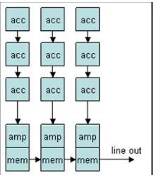
The charge-coupled device (CCD) was invented around 1970. As shown in Fig.1.1, a CCD transfers the acquired analog charge (electrons) from one photodetector through other photodetectors across the chip. This operation is called a “shift,” mak-ing CCDs a type of shift register. A CCD uses a MOS photodetector for photon ac-quisition and for readout tasks. Note that the charge is transfered without creating a voltage. Only in the readout stage does the charge get converted into a voltage.
Fig. 1.1 Charge readout from
a CCD, a shift register.
There are three types of readout architectures: (1) Full-frame devices consist of large charge accumulators and minimal additional circuitry around every pixel. They require a mechanical shutter because the entire sensor area is exposed to the light and would continue to accumulate charge as the image is transfered out. (2) Frame transfer devices have half the CCD covered with an opaque material. The electronic shutter moves the charge “under cover” and slowly reads it out. Full-frame and frame transfer devices have the disadvantages that the charge needs to be shifted down the entire sensor array. Pixels in the first rows hence incur a larger amount of readout noise. To obtain interlaced output from a frame device, every other row must be discarded before data serialization. This gives these devices different char-acteristics than vidicon tubes of comparable specs, namely shorter integration time and reduced light sensitivity. (3) Interline transfer devices have storage circuitry at every other line or column, avoiding this large shift noise accumulation and allow-ing for fast readout. Interline transfer devices can be read out in arbitrary row order, for example, in interlaced order. This makes them particularly well suited for analog output.
A disadvantage of CCD sensors is that the photonic element can overflow: too bright a light source causes charge to spill into neighboring accumulators which, in turn, causes bright blobs called blooming or, during readout, vertical lines called smear.
Fig. 1.2 shows the pixel flow from photon to digital signal. This is a generalized pipeline, applicable to both CCD and CMOS sensors with the noted differences.
Fig. 1.2 Overview of pixel acquisition in a sensor. Only a CCD performs the electron shift
func-tion, whereas a CMOS sensor converts electrons into voltage on a per-pixel basis. Only the CMOS sensor has a row-select function.
1.2.3 CMOS Sensors
The so-calledactive pixel sensor(APS) dedicates circuitry to every pixel to convert the electric charge into voltage. This type of image sensor is typically manufactured with CMOS transistors, hence its more common name “CMOS sensor.” Every pixel has its own amplifier, typically three or more transistors (see Fig. 1.3). Therefore, an important issue with CMOS imagers is the pixel fill factor—that is, how much of the space that one pixel takes up is dedicated to photon acquisition and how much is spent on related hardware such as charge conversion, amplification, and readout circuitry. Good fill factors for CMOS sensors are 50% or above, but they can be much lower. A CCD has close to a 100% fill factor. Multilayered sensor arrays, called “stacked dies” or 3D VLSI as opposed to planar VLSI technology, can offset some of these disadvantages and achieve higher fill factors for CMOS sensors.
Fig. 1.3 Schematic of one pixel of a CMOS active pixel sensor. The photodetector accumulates the charge that can be measured with the transistor Ms f. The
measurement is read out on the column line if the row is selected via transistorMsel. A
charge reset is triggered with transistorMrst. Retrieved from
http://commons.wikimedia.org on 17 April 2008.
Dark scenes therefore require a higher gain, which introduces noise in the readout process.
Similar to a memory chip, there is a criss-cross grid of readout lines running across the image array. The row-select lines select one of the array rows. The column lines transport the pixels’ activation down to the readout electronics, typically an amplifier followed by a multiplexer. In contrast to CCDs, the activation in a CMOS is voltage rather than charge, and it is transported to the readout directly, without requiring a shift through all pixels in the same row below the current pixel.
For a more detailed discussion of active pixel sensors see, for example, Eric Fossum’s articles [3, 6]. Dave Litwiller at DALSA has some excellent articles com-paring CCDs and CMOS sensors [4, 5], accessible via their web site at [11].
1.2.4 Readout and Control
Image sensor control and pixel readout is facilitated with on-chip logic. This cir-cuitry drives the reset signal lines, initiates the charge transfer, chooses one row-select line at a time, sets the gain level, packages the outgoing pixel data and re-sponds to input control commands. These commands are specified in protocols and sent over a control bus to the sensor (see the next section). The sensor reacts by setting control registers accordingly. Its logic reads out the registers regularly, for example, during the reset cycle, so that the next frame that is to be captured con-forms to parameters such as exposure, windowing, and gain. Permissible times for the arrival of control packets and their synchronization with frame readout differ between the various manufacturers and from chip to chip.
the color information for one line since (e.g., for a Bayer pattern) the red and blue pixel filters are applied on alternating lines.
The next section discusses the physical connection and the protocol used for communication between the sensor chip and the control and image processing hard-ware.
1.3 Interconnects to Sensors
When considering the design features associated with the interconnection of an im-age sensor to a host computer, several issues are critical.
• interface width—should the interface be parallel or serial?
• direction of flow—should the interface be unidirectional or bidirectional? • power—will it be possible to power the imager through the interconnect? • distance—what is the maximum cable length?
• connectors, cabling, and signal integrity—what connectors are available and which should be used?
With an imager delivering 10–14 bit pixels at rates in the range of 50 million pix-els per second and considering power limitations and signal integrity, it seems most appropriate to choose a serial interface that uses low-voltage differential signal-ing (LVDS). The availability of high-quality LVDS transceivers intended for PCI-Express and other high-speed serial interfaces, particularly those with integrated se-rializer/deserializer (SERDES) circuits makes this part of the design rather straight-forward.
To further leverage the computer industry’s developments and standards in the area of high-performance serial interfaces it seems prudent to incorporate pre-built cables and connectors that were designed for the IEEE-1394 (aka FireWire) stan-dard. The FireWire cables and connectors contain six wires: two to supply DC power across the interface and two twisted pairs to support bi-directional differential sig-naling.
Fig. 1.4 shows the structure of typical link hardware. Note that in addition to the two differential pairs shown in the cabling, there are two power wires as well. This facilitates the delivery of DC power to the imager subsystem. Though the principal flow is from imager to computer, the LVDS transceiver interface is bidirectional so as to provide for control and initialization of the imager. Most imagers have control interfaces such as I2C (Inter-Integrated Circuit bus, pronounced i-squared-c).
Image
sensor
:
LVDS
2
LVDS
:
2
Acquisition
Interface
up to 10 m
Fig. 1.4 Structure of a typical link. Power connections are not shown.
the LVDS physical layer transceivers to packetize and de-packetize the data flowing across the link.
Fig. 1.5 shows a candidate packet layout that supports imager pixel widths up to 14 bits. In the given packet layout there would be up to 4 packet types and there could be different layouts for the incoming vs. outgoing data directions if needed. The two packet types detailed in Fig. 1.5 would be appropriate for the host-to-imager direction, providing 16-bit register data to be written into the imager register number given. Note that the 16-bit data field has been split between two packet types with 14 bits in the (0,1) packet type and the two highest-order bits in the (0,0) packet type. Such a layout facilitates easy packet decoding and multiplexing in a CPLD or FPGA located on each end of the cable. In the opposite direction (i.e., imager-to-host), packets could similarly be defined to support either up to 14-bits of pixel data per 16-bit packet type or, if needed, a two-type combination with 16 bits of pixel data together with imager status.
packet type
content interpreted based on packet type
0 1
0 0 register number (8 bits) pixel or register data (up to 14 bits wide)
data
imager control or status
Fig. 1.5 Candidate packet layouts using 2-bit packet type code in every 16-bit packet.
line code [10]. This code is used for DC balance; it keeps the running disparity between the number of 1’s vs. 0’s no greater than two and guarantees no occurrence of five or more consecutive 0’s or 1’s in the entire frame. Each 8-bit data byte is encoded using 10 bits on the line with the extra code space used to achieve DC balance and with certain reserved code words defined to facilitate link management.
1.4 Image Operations
Before discussing the various types of processing hardware available for embedded vision systems, it helps to keep the objective in mind: processing image data with different operations and algorithms. This section addresses the question of how well certain operations are suited to embedded implementation.
An algorithm’s speed performance on a DSP or FPGA often differs vastly from its performance on a general-purpose processor (GPP/CPU). The following algo-rithm characteristics lend themselves to execution in special hardware:
• data streams and sequential data access, as opposed to random access, • multiple, largely independent streams of data,
• high data rates with few instructions per datum, • a fixed data packet size, or a size below a tight bound,
• stream computations that can be broken up into pipeline stages, that is, the same (possible parameterized) set of computations can be applied to lots of data, • the operations require only fixed-precision values (integer or fixed-point
frac-tions),
• algorithms are parallelizable at instruction and module level, that is, little between-stream communication is necessary.
Desirable operations to be executed on high-performance hardware in the em-bedded system are typically lower-level functions that pre-process the image for further high-level analysis and might include:
• convolution/cross correlation, 2D and separable filters (Gaussian, wavelets etc.), • subsampling at regular intervals,
• Canny edge detection,
• sum of absolute differences (SAD) of an image region of interest (ROI) with a stored patch,
• edge orientation and histogram calculation, • integral image calculation,
• online calculation of global or ROI statistics: min, max, mean, or variance, higher-order moments,
• online Bayer sample pattern conversion into RGB, HSV, GRAY, etc. (depending on camera color pattern this requires a one-line buffer)
• online color space conversion (RGB2GRAY, RGB2HSV).
that is slid over the entire data. This is easily possible for simple operations such as the minimum or mean value, but only possible through approximation for median calculation, for example.
Table 1.1 shows common operations and the complexity of their data access pat-terns. For the best speed and memory performance, the algorithm accesses only a single pixel at any one time, and the sequence of pixel accesses is know before-hand. On the opposite end of the spectrum are algorithms that require large amounts of data for the calculation of one result and their data access pattern is not known before hand, for example, when it is dynamically dependent on the result of previous calculations. Hence, the speed and memory complexity of the methods mentioned in Table 1.1 increases from top to bottom. Some algorithms create a data space that is accessed in subsequent passes, rather than accessing the image space multiple times.
1.5 Hardware Components
A perusal of available commercial building blocks yields a rich selection of general-and special-purpose microprocessors, field-programmable arrays, general-and memories from which the processing unit of an embedded vision system can be realized. Re-cent experience by the authors with DSPs and FPGAs has yielded some designs that have proven to be very robust, while at the same time flexible and highly adaptive. We briefly describe the main characteristics of hardware components in the follow-ing sections, from rather general-purpose to system-specific chips.
1.5.1 Digital Signal Processors
A digital signal processor, or DSP, is similar to a general-purpose processor (GPP) in many aspects. It has fixed logic, that is, the connections between logic gates cannot be changed. It provides a fixed instruction set (ISA) to the programmer, and it expects a program in this ISA that it will then execute in a sequential manner (as opposed to dataflow-driven). Most DSP ISAs exhibit a similar structure as GPP ISAs, complete with arithmetic and logic instructions, memory access, registers, control flow, and so on.
simultane-Table 1.1 Data Interdependency in Image Space
Pixel processing: a single pass over the image is sufficient, and a pixel’s new value is only determined by exactly one source pixel value.
N-pass: multiple passes over the image and data space are nec-essary; however, only one source pixel value determines the new pixel value.
• count, min, max, avg, stddev
• histogram equalization or histogram matching
• Hough transforms
Fixed-size block access: the values of pixels in an area of known and fixed size determines the output value.
• morphology
• convolution, filtering
• pyramids
• wavelets
• KLT (Lucas-Kanade) feature tracking
Data-independent, global access: multiple source pixel values from pixels all over the image determine the outcome of the op-eration. The access pattern is known, however.
• Viola-Jones
• warping or remapping for distortion correction
Data-dependent, random access: multiple source pixel values from pixels all over the image determine the outcome of the operation. The access pattern is determined by the values read from the source pixels.
• naive flood fill • contour finding
the same VLIW. This constraint is relaxed even further in so-called MIMD ma-chines (multiple instruction, multiple data), where multiple identical processors can independently execute arbitrary instructions on non-dependent data.
You might note that modern CPUs and their multiple-dispatch (superscalar) pipelines do exactly that—schedule multiple instructions concurrently. With DSPs, however, there is no such intelligent pipeline. Instead, the burden of scheduling is on the compiler: it has to co-schedule instructions for independent data operations and optimize the packing of instructions in width (e.g., four instructions per word) and in sequence (control flow). DSPs do not perform such complex CPU operations as branch prediction or instruction reordering. Here, too, the compiler has to perform the optimizations.
DSP programs are relatively small programs (tens or hundreds of LOC), with few branch and control instructions, as opposed to entire operating systems running on general-purpose CPUs. Frequently, a single, tight, and heavily optimized loop is executed once for every data element or set thereof. Fig. 1.6 shows how the serial-ized pixel data is streamed through a DSP with a simple one-dimensional smoothing filter.
Fig. 1.6 One-dimensional
fil-ters such as Gaussian smooth-ing can be implemented in even the simplest DSPs. Here, pixels are fed into a pipeline that calculates a weighted sum on a five-pixel window into the pixel stream. The height of the gray curve depicts the weights.
Since DSPs usually execute small programs on huge amounts or endless streams of data, these two pieces of information are stored in separate memory blocks, often accessible through separate buses. This is called aHarvard architecture, as opposed to the GPP’svon Neumann architecture, in which both program and data are stored in the same memory. Because the program does not change (firmware!), many DSPs provide on-chip ROM (typically in the order of 10 kB) for program storage, and a small but efficient RAM hierarchy for data storage. Frequently, an embedded system also includes a separate non-volatile memory chip such as an EEPROM or flash memory.
embedded vision systems: programmability, direct memory access (DMA) architec-tures, some level of parallelism (VLIW or SIMD), low power and low cost.
Example vision systems using DSPs are discussed in Chapters 4 and 9. Manufac-turers of DSPs include Agere Systems, Analog Devices, Infineon, Lucent Technolo-gies, Equator TechnoloTechnolo-gies, Freescale Semiconductor (formerly part of Motorola), NXP (formerly part of Philips Electronics), Texas Instruments, and Zilog. Most of these manufacturers also offer DSP development boards specific for image process-ing and computer vision, complete with the required auxiliary chips, with cameras and software. Those are an ideal starting point for an experimental embedded vi-sion system. Bruno Paillard wrote a good introduction to DSPs that can be found at [12]. A good textbook resource is Lynn and Fuerst’sIntroductory Digital Signal Processing with Computer Applications.The USENET group comp.dsp might also be of interest to the reader.
1.5.2 Field-Programmable Gate Arrays
A field-programmable gate array, or FPGA, is a semiconductor in which the ac-tual logic circuit can be modified to the application builder’s needs. The chip is a relatively inexpensive, off-the-shelf device that can be programmed in the “field” and not the semiconductor fab. It is important to note the difference between soft-ware programming and logic programming, or logic design as it is usually called: a software program always needs to run on some microcontroller with an appropriate instruction set architecture (ISA), whereas a logic programisthe microcontroller. In fact, this logic program can specify a controller that accepts as input a particular ISA, for example, the ISA of an ARM CPU, effectively turning the FPGA into an ARM CPU.
This is a so-calledsoft core, built from general-purpose logic blocks. These soft cores, or better the right to use the intellectual property, can be purchased from com-panies such as Xilinx, Inc., and Altera Corporation. They are then “downloaded” to the FPGA where they implement the desired functionality. Some of the modern FPGAs integrate platform- or hardmultipurpose processors on the logic such as a PowerPC, ARM, or a DSP architecture. Other common hard and soft modules include multipliers, interface logic, and memory blocks.
Thelogic designdetermines the FPGA’s functionality. This configuration is writ-ten to the device and is retained until it is erased. To be precise, there are three types of FGPAs: antifuse, SRAM, and FLASH. Antifuse chips are not reprogrammable. FLASH (EPROM) is also nonvolatile, meaning that the logic design stays on the chip through power cycles. It can be erased and reprogrammed many times. SRAM programming on the other hand is volatile; it has to be programmed at power on.
in the FPGA and then perform pixel operations on the entire region simultaneously (see Fig. 1.7). FPGAs can achieve speeds close to DSPs and ASICs, require a bit more power than an ASIC, have much lower non-recurring engineering (NRE) costs, but higher volume prices than ASICs.
Fig. 1.7 Region of interest
(ROI) processing in hardware (FPGA) after spreading the image over the chip.
Algorithm developers and software engineers are usually trained on a sequential model. That and the flexibility of logic circuitry make parallel designs on FPGAs a challenging task, particularly because the best implementation is often not intu-itively apparent. One of the first difficulties is dividing the responsibilities between the FPGA and a GPP, and between the FPGA’s core CPU and into possible other chips on the platform. Common “hardware description languages” for logic design are Verilog and VHDL and the topic of many engineering courses and books.
FPGAs are a great resource for parallelism and offer tremendous flexibility in the embedded vision processing system. On the other hand, large FPGAs are quite power hungry and their clock rates are lower than a typical DSPs’ clock rate. A wide variety of field-programmable array chips are available on the commercial market today. The optimal choice for an embedded vision system is a combination of a single FPGA with sufficient general-purpose I/O resources to handle the imager’s incoming and outgoing interfaces plus a 64-bit interface to/from the DSP. An equally important selection criterion will be the amount of embedded FPGA memory as well as the package. Most FPGAs have an abundance of I/O capability as compared with internal logic so it is probable that an optional 32-bit SDRAM interface may also be possible. Such an interface in an embedded vision system would provide the FPGA with private access to its own storage area at the cost of access time and added FPGA complexity. The plentiful I/O resources are also used to let FPGAs control the input gates of other onboard chips.
1.5.3 Graphics Processing Units
Interface standardization in the world of computer graphics took a long time to come together. Its need was seen since the 1970s [8], but it wasn’t until the 1990s that SGI and Microsoft were successful publishing their respective standards OpenGL and Direct3D. The effect on the graphics hardware and software industries was im-mense, as billion-dollar-strong markets indicate. The special processors developed for graphics rendering, called graphics processing units, or GPUs, have surpassed transistor integration densities of consumer general-purpose processors (GPPs or CPUs). Many graphics operations lend themselves very well to parallelization due to their mutual independence. This led to the development of parallel processing units in GPUs, called shaders. The most recent GPUs havehundredsof shader pro-cessing units that can each perform operations on different sets of data, producing independent results. Typically, subgroups of these shaders run in a SIMD mode, executing the same instruction at the same time on different data. In contrast to DSPs and similar to CPUs, the GPU takes care of scheduling and synchronization of the tasks assuming, however, that their executing is largely independent from one another.
The so-called shader programs are short snippets of code that have to conform to certain restrictions. While more recent specifications permit relaxation of some of these, traditionally shader programs may not have dynamic branch instructions, are limited to floating-point operations, and may not exceed 100 or so instructions. Shader programs are intended either for vertices or for fragments. Vertices are points in 3D space, and vertex shaders perform operations such as determining vertex position or vertex color with geometric calculations. Fragment shaders (or pixel shaders), on the other hand, perform operations on pixels in a 2D space, such as texturing or color blending. It is expected that one common type, geometry shaders, will unite the functionality of vertex and fragment shaders.
The programming model for shaders is traditionally data-driven. For this and other reasons, to utilize GPUs and shaders for tasks such as image processing or computer vision, data has to be packaged to act like graphics data, and operations have to be disguised as graphics operations. Higher-level languages that are com-piled into shader languages have sprung up, however, making programming vastly easier and program conversion more and more automatic. Examples are Nvidia’s Cg, Microsoft’s HLSL, and most recently Nvidia’s CUDA development environ-ment. CUDA (which stands for computer unified device architecture) clearly shows the trend of GPU utilization for applications other than computer graphics: along with a C-style language definition and compiler, it provides a general matrix calcu-lation library (BLAS) and a fast Fourier transform implementation, code for image convolution and other image processing tasks.
research, coined GPGPU which stands for general-purpose computation on GPUs, to use these device as coprocessors for computer vision and other applications be-yond graphics. GPGPU is driven with the availability of high performance, low-cost GPUs; they are now standard components in devices such as our portable computers as well as mobile handsets. GPUs are briefly covered in Chapter 11 with respect to mobile phones.
Designers must still consider the tradeoffs between power and performance as higher-end GPUs tend to demand high-power resources. Very often, GPUs are matched with specialized memories (VRAM or video RAM) that offer higher band-width at a higher system cost. To realize the full benefits of GPUs, programmers must properly partition their algorithms for the GPUs since there may be setup penalties to initiate tasks on GPUs. GPUs are extremely powerful resources and we are only seeing the beginning of their utilization for vision tasks. It is up to the system designers to consider their match to the characteristics required for many embedded vision systems: low power requirements, low volume cost, and special-ization to the task at hand. The following section discusses chips at that end of the spectrum: custom-developed for a specific tasks.
1.5.4 Smart Camera Chips and Boards
An application-specific integrated circuit (ASIC) is a chip that is designed and opti-mized for one particular application. The logic is custoopti-mized to include only those components that are necessary to perform its task. Even though modules are reused from ASIC to ASIC just like FPGA modules, a large amount of design and imple-mentation work goes into every ASIC. Their long production cycle, their immensely high one-time cost, and their limited benefits in speed gains put them slightly out of scope of this tutorial. Contributing to the high cost, they need to be respun if the design changes just slightly, costing months and usually hundreds of thousands of dollars. Their benefits lie in potential power savings and a decreasing asymptotic cost (with high unit numbers).
ASICs, processors, SoCs, and chip sets that directly support higher-level com-puter vision tasks come in various flavors, from CMOS image capture chips that include one or multiple small processors to framegrabber PCI boards with multiple full-scale CPUs. Some examples of devices and companies that manufacture them are:
• OmniVision Technology in Sunnyvale, CA, builds still camera chips (CMOS) with integrated processing power.
• NuCORE Technology in San Jose, CA, offers a digital image processor with an “object detection engine” for real-time face detection.
• Zoran Corp. in Sunnyvale, CA, sells the COACH image processing ASIC for digital cameras, which can perform motion stabilization.
• Matrox in Dorval, Canada, also manufactures frame grabbers, for example, the Odyssey Xpro+ contains a G4 PowerPC, a Matrox ASIC, and an Altera Stratix II FPGA.
• Anafocus, a spin-off from the Universidad de Sevilla in Spain, builds mixed-signal CMOS chips (ACE4K, ACE16K, Eye-RIS) with an image acquisition array, digitally programmable analog signal processors, and DSP functional-ity [1, 7].
• Eutecus in Austin, TX, creates the “Bi-i” smart camera from the ACE16k v2 chip and a Texas Instruments DSP.
• Mobileye in Amstelveen, Netherlands, sells the EyeQ CMOS ASIC which houses two ARMs and four processors that are specialized for image processing tasks. • Sarnoff of Princeton, NJ, created the Acadia ASIC (see van der Wal et al. [9] and
at [14]), a highly specialized image processing chip.
• Pixel Velocity in Ann Arbor, MI, is developing a smart camera that uses 2-6 PowerPC405 (each running at 300MHz) and one Xilinx FPGA to crunch image data faster than a single CPU.
• IQinVision in San Clemente, CA, sells video surveillance systems and software such as face detection that can be uploaded on their IQeye smart cameras.
1.5.5 Memory and Mass Storage
In addition to a processing unit, an embedded vision board will need a reasonably large memory with width and access time commensurate with the required image stream acquisition, processing, and storage needs of the vision application. The de-tailed selection of a particular type of memory (SRAM, DRAM, SDRAM, flash, etc.) is largely driven by space and capacity concerns and, to a lesser extent, by cost. While a multiported SRAM would be best for creating an easy-to-use shared mem-ory located between a DSP and an FPGA, for example, such a memmem-ory would likely be too small in capacity, far too high in cost, and too large in physical size due to the number of I/O pins required. An SDRAM is more appropriate for most vision applications. It is likely to be small enough in physical size while large enough in storage capacity to fit the bill. Such a memory is significantly more difficult to share, however, since its access involves a dedicated SDRAM controller. Luckily, such a controller is usually integrated within a DSP and SoC, and available as soft core for FPGAs. All SDRAM memory accesses need to originate at the SDRAM controller and, thus, the DSP would become the hub (and, unfortunately, also the potential bottleneck) for all memory activities.
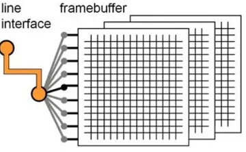
Full frame storage in memory (a frame buffer, see Fig. 1.8) permits arbitrary op-erations on the image with no predetermined pixel access order. Higher-level pro-cessing that does not concern pixel data directly often involves higher-dimensional data in a feature space rather than the two- or three-dimensional image data.
Fig. 1.8 Frame buffer storage
of the image, permitting random pixel access.
Mass storage units are available (SATA or PATA disk drives) and would be se-lected based upon the needs of the main application. Flash-based disk-drive units are attractive from a weight, power, and speed perspective though their capacity is lim-ited and their cost is higher than traditional magnetic disk technology. It is often the case for embedded systems that very little mass storage is required—just enough for booting the O/S and holding a small file system—though for vision systems, particularly those involving video, mass storage needs can be substantial.
1.5.6 System on Chip
A system on chip (SoC) contains all essential components of an embedded system on a single chip. The definition is blurry, as sometimes this only refers to the digital components and sometimes it includes analog components. DSPs have an increas-ing amount of peripherals included on the die as well, warrantincreas-ing the inclusion in this category. Most SoCs have a GPP such as an ARM, MIPS, PowerPC, or an x86-based core at their heart, supplemented by a DSP. What makes these chips an entire system are the inclusion of a bewildering array of peripherals. In addition to standard microcontroller components (busses, clocks, memory), typical integrated components are:
• Ethernet MAC
• PCMCIA
• USB 1.0 and 2.0 controller • Bluetooth
• RS232 UART • IrDA
• display interface • flash memory interfaces • ADCs and DACs
Systems on a chip are of particular interest to highly integrated devices such as mobile phones, portable DVD and mp3 players, set-top-boxes and cable modems. Many SoCs have dedicated circuitry for video processing, which usually means hardware support for decoding from (and sometimes for encoding into) the various video formats, including MPEG2, MPEG4, and H.263. An extensive list of SoCs can be found at [15].
1.5.7 CPU and Auxiliary Boards
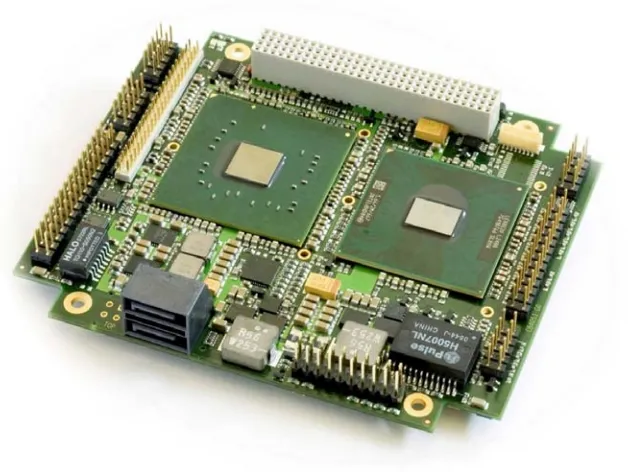
Many experimental and prototype embedded systems employ a general-purpose host computer at the highest level. This machine can run the overall application. In addition it can stage and boot the attached DSP and FPGA hardware. Volatile FPGAs and the DSPs need their logic and programs loaded. In production systems, this frequently resides in an internal storage such as Flash or a small disk. With a host computer system, the host boots first. Once running, it then initializes and loads the FPGA(s), loads the DSP(s) and starts their programs. After that, software and hardware protocols are used to keep all inter-system transactions orderly. Programs running in the DSP (via the FPGA) can initialize and control the imager. Due to size and power concerns the logical choice for the host is often a PC/104 form factor [2]. Systems with significant capability (e.g., with a dual core x86 CPU, 2Gb main memory, and all of the traditional PC peripheral interfaces) are available in this form factor; Fig. 1.9 shows such a system. With an on-board compact PCI bus connector, it becomes feasible to attach a custom processing unit for vision processing, making development and debugging much easier. The power needs of such a system are a concern, however, particularly for embedded systems that run from battery power. The power budget for the overall system described here (i.e., host plus processing board and imager) is 50W.
1.5.8 Component Interconnects
Any designer of a custom high-performance embedded system must pay careful attention to the interconnections between and among components and to connec-tors. Fortunately, the computer industry, via its international standards committees, has been extremely helpful in this regard. It is precisely because of bus and point-to-point signaling standards like PCI, compact-PCI, FireWire, USB, I2C, and
Fig. 1.9 PC/104 host computer (used by permission of Adlogic, Inc.).
compact-PCI connectors and the PCI protocol to attach the DSP/FPGA resources to the host system. The connection between the imager subsystem and the DSP/FPGA board would be made from LVDS transceivers and would use FireWire connectors and cables (but would not implement any of the IEEE 1394 FireWire protocols).
1.6 Processing Board Organization
The previous section discussed the building blocks and architectural issues sur-rounding an embedded vision system. Some recommendations for prototype em-bedded computer vision systems have emerged from that section, namely: PC/104 form factor host, compact PCI bus signaling to/from an attached PC/104 processing board with DSP/FPGA and memory, attachment to an imager subsystem via cus-tom LVDS interface. Given these recommendations, several DSP-FPGA-memory organizations are possible. The optimal one for a vision system depends on the computational needs of the application and are discussed in this section.
temporary data will normally be quite limited in size with no possibility for expan-sion. Today’s DSPs often contain an integrated SDRAM controller. A large system memory is available via such an external interface. There can also be memory re-sources within the FPGA and these will typically be used to stage and support the data for highly parallel computations within the FPGA. Such FPGA memories are quite limited in size.
Additional FPGA-specific memory can be added by incorporating an SDRAM controller within the FPGA. This method can provide for a significant amount of storage but any such memory would remain private to the FPGA rather than shared with the DSP. More ideal would be a multiported SRAM located between and shared by the DSP and FPGA. Except for a very small one, such a setup would be pro-hibitively large, expensive, and cumbersome due to the number of pins and traces involved with the address and data buses. Yet another choice might be an SRAM connected to a bus that was shared between the DSP and FPGA. This might be workable though the complexities arising from reserving and releasing bus master-ship would take away from overall utility and the cost and size for an SRAM in the megabyte size range would start to be prohibitive. Making this approach work ef-fectively and efficiently would be difficult to achieve with available DSP and FPGA resources.
The chosen memory organization is depicted in Fig. 1.10. This approach uses a large SDRAM attached to the DSP via its integrated SDRAM controller with a wide bus-style attachment to the FPGA via a separate external memory space of the DSP. If a DSP with multiple DMA controllers is used then a few of the DMA units can be allocated to the task of moving pixel rows or columns or other chunks of related data between the DSP and FPGA over the external memory bus.