ARAHAN KEPADA CALON :
Peperiksaan Semester Pertama
Sidang Akademik 1996/97
Oktober/November 1996
BEE 370 -
Mikropemproses
n
Masa
[2
jam]
Sila pastikan bahawa kertas peperiksaan ini mengandungi LAPAN
(8)
muka surat berserta
LAMPIRAN (9) muka surat bercetak
~anENAM
(6)
soalan sebelum anda memulakan peperiksaan
ini.
Jawab EMP AT (4) soalan.
Agihan markah bagi soalan diberikan di sut sebelah kanan sOidanberkenaan.
Jawab semua soalan di dalam Bahasa Malaysia.
1.
(i)
-2-
[BEE 370]
Mikropengawal
Iembedded' bagi aplikasi bolehgerak yang menggunakan bateri
memerlukan mekanisma pengurusan kuasa yang efisien. Bincangkan ciri-ciri
pengurusan kuasa yang terdapat dalam mikropengawal yang biasa digunaka!".
Huraikan contoh pengunaan salah satu ciri tersebut.
Embedded microcontrollers in mobile battery-powered applications require an efficient
power management mechanism. Discuss the power management features available in typical
microcontrollers, with an example application.
(20%)
(ii)
Pehjimatan kuasa adalah berkadaran dengan
kekerapan
mikropengawal
dimasukkan ke dalam mod 'tidur' selama masa yang ditetapkan, apabila
keperluan pemprosesan adalah rendah ataupun dihentikan buat sementara waktu.
Tunjukkan bagaimana ini dilakukan bagi mikropengawal 8051
Power conservation is directly proportional to the number of times you can put a
microcontroller to 'sleep' for a pre-determined period, when processing demand
is
low or
temporarily terminated. Show how this
is
done for an 8051 microcontroller when
(a)
mengunakan pemasa dalarnan.
using the internal timers, and
(b)
dengan litar 'wake-up' Iuaran.
with external 'wake-up' drcuit.
Kod aturcara perIu diberikan.
Program codes must be given.
(40%)
(iii)
Bagi kebanyakan aplikasi
'embedded',
RAM mikropengawal mengandungi
maklumat kritikal yang perlu disimpan sekiranya berlaku kehilangan bekalan
kuasa. Huraikan dengan mendalam (dari segi perkakasan dan perisian) bagaimana
ciri ini dilaksanakan jika peranti 87C51 digunakan dalam rekabentuk berkenaan.
For most embedded applications, the microcontroller RAM containing critical infonnation
must be saved in the event of power loss. Describe in detail (both hardware and software)
how this feature can be implemented
if
an B7C51 microcontroller
is
used in the design.
372
(40%)
3/--3-
[EEE370]
2.
Suatu sis tern pengumpulan data 64-saluran 8-bit diperlukan hagi mengawasi parameter ..
parameter enjin bagi sebuah kapal besar. Adalah dikehendaki supaya beban
pengumpulan data tersebut diagih-agihkan antara beberapa pemproses hamba, dan
dikumpulkan oleh satu pemproses tuan, kesemuanya dihubungi oleh satu rangkaian
multi-drop'
RS-485.
Pemproses tuan boIehlah seterusnya menghantarkan kesemua
rnaklumat yang dikumpul ke satu komputer pusat untuk tujuan papa ran, rekod dan
analisis.
A 64-channel 8-bit data acquisition system
is
required for monitoring the engine parameters of a
large ship.
It
is
desired that the
data
acquisition tasks be distributed among several slave
microcontrollers, and collected by one master unit, all linked by a multi-drop RS-485 network.
The
master can then pass on the collected data
to
a central
PC
for display, logging and analysis purposes.
(i)
Berikan garnbarajah biok bagi keseluruhan slstem tetsebut, dengan huraian
lengkap.
Produce a hardware block diagram for the overall sys tem,
wi
th detailed description.
(30%)
(ii)
Huraikan dengan mendalam perkakasan bagi modul mikropengawal hamba dan
tuan.
Provide a complete hardware description of the slave and master microcontroller modules.
(30%)
(iii)
Terangkan dengan lengkap bagaimana anda melaksanakan protokol perhubungan
diantara modul-modul hamba dan tuan. Berikan contoh aturcara untuk
memindahkan data dari modul hamba ke modul tuan.
Explain in detail how you would implement the communication protocol between the slaves
and
the
master modules. Give an example program to transfer data from a slave to the
master.
(40%)
...
4/-373
3.
(a)
-4-
(EEE370]
Bincangkan masalah-masalah
yang
perlu dihadapi apabilamerekabentuk sistem
mikropengawal bagi kegunaan dalam persekitaran yang mempunyai bising
elektrik.
Discuss the problems involved in designing microcontroller systems for applications in an
electrically noisy environment.
Perkara-perkara berikut perIu dibincang dengan mendalam:
The
following points must be discussed in detail:
(i)
jenis dan sumber bising elektrik
types and sou rces of electrical noise
(ti)
kesan bising
effects of noise
(iii)
penangkisan
shielding
(iv)
pembumian
grounds
(v)
pengagihan bekalan kuasa dan 'decoupling'
power supply distribution and decoupling
(vi)
strategi pembentangan PCB.
pcb layout strategy
(60%)
(b)
Pemasa 'watchdog' adalah berguna untuk membolehkan pemproses pulih-semula
dari kesilapan pelaksanaan aturcara. Walau bagaimanapun, tiada sekim 'watchdog'
yang dapat memberi aras keyakinan 100%. Oleh itu, dalam aplikasi kritikal,
bagaimanakah kebolehpercayaan 'watchdog' dapat ditingkatkan?
(Berikan
sekurang-kurangnya 4 teknik).
Watchdog timers are useful to help processors recover from software upsets. Hawever, no
watchdog scheme can provide 100% confidence. Therefore, in critical applications how can
you increase the reliability of the watchdog itself? (Give at least
4
possible techniques).
(40%)
...
- 5 -
[EEE370]
4.
Rekabent1J}c~an
5uatu peranti pemasa berasaskan mikrQpengawal, yang mempunyili
spesifikasi seperti berikut:
Design a microcontroller-based timer device, with the following specifications:
•
2 pemasa
Icountdown', hanya satu aktif pada sesuatu ketika.
2 independent countdown timer, but with only one being active at any particular time.
•
Setiap pemasa membilang sebanyak 100 jam maksimum.
Each timer can have a maximum count of 100 hours.
•
Butang
Imula-henti' yang berasingan bagi setiap pemasa.
A
separate start-stop button for each timer.
•
Saki masa boleh didapati bagi mana-mana pemasa, walaupun salah satu sedang aktif.
A
balance check can be done on any of the timers, even when one of them is counting.
• I
Alarm' dibunyikan apabila bilangan sifar dicapai oleh mana-mana pemasa.
An alarm
is
sounded when zero count is reached by any of the timers.
•
'Keypad' diperlukan untuk mengsetkan pemasa.
A keypad is required for setting the timer.
•
LED 7 -segmen digunakan sebagai paparan
GAM:
MIN).
7-segment LEDs are used for
the
display. (Hours: Min)
•
Bekalan kuasa bateri
Battery powered
•
Data pemasa disimpan apabila peranti dimatikan.
Timer data saved when device is off.
•
Mempunyai antaramuka RS232
RS232 serial interface
Maklumat berikut diperlukan:
The following information
is
required:
(i)
Gambarajah blok bagi pemasa berkenaan, dengan penerangan lengkap bagaimana
setiap fungsi dilaksanakan. Peranti-peranti yang digunakan juga perlu dijelaskan.
Block diagram of the proposed timer, with detailed explanation of how the functions are
implemented. The devices to be used must be clearly identified.
375
(40%)
6/ 6 6/
-(ii)
Gambarajah skematik perkakasan.
(iii)
Hardware schematic diagram
Carta alir bagi keseluruhan perisian.
Flowchart for the complete software.
[EEE 370]
(30%)
(30%)
5.
Suatu perantimasukan perlu diantaramukakan ke pencetak siri.Peranti ini mempunyai
satu talian masukan, RUN, yang apabila 'tinggi', mengaktifkan peranti
berken~an.Peranti
tersebut kemudiannyamengeluarkan bait-bait data secara tak-segerak pada 8 talian DATA.
Ianya juga mempunyai satu talian status data sah,
DA
V, yang menunjukkan data sah,
setiap kali status berubah dari '1' ke '0'. Talian-talian RUN, DAV dan keluaran DATA
sajalah merupakan sambungan kepada peranti tersebut. Masukan dan keluaran adalah
TIL.
An input device is to be interfaced to a serial printer. The device has one input, RUN, which when
high, operates
the
device.
The
device then outputs bytes of data asynchronously on its
8
data lines. It
has one data valid status,
DA
V, which indicates valid data each time
it
makes a
'1'
to '0' transition.
The RUN, DAV and data output are
the
only connection to the device. The input and output aTe
TTL.
Antaramuka pencetak siri pula terdiri dari 3 tali an, Rx, Tx dan GND. Ianya dikendalikan
pada kadar 300 baud, tanpa jabat-tangan.
The
printer's serial interface consist of
3 lines, i.e Rx, Tx
'
and GND.
It
is to be operated at 300 baud,
wi th no handshaking.
Terangkan bagaimana satu cip mikropengawal8751 dapat dijadikan sebagai antaramuka
diantara peranti masukan berkenaan dengan pencetak.
Show in detail how a single-chip
8751
microcontroller can be used as the interface between the device
and the printer.
Perkara-perkara berikut perhl diberikan:
The
following information
is
required:
...
-7-
[EEE 370]
(i)
Prinsip operasi, beserta gambarajah blok.
Detailed principle of operation, with block diagrams.
(40%)
(ii)
Skematik bagi antaramuka.
Complete schematic drawing for the interface.
(30%)
(iii)
Perisian pengawalan yang lengkap.
The complete control software, with comments.
(30%)
6.
Suatu peranti ingatan (X24C44) diantaramukakan ke mikropengawal 8051 seperti
ditunjukkan· dalam Rajah 1. Data untuk peranti berkenaan diberikan dalam Lampiran 2.
A
memory device
(X24C44)
is interfaced to an 8051 microcontroller as shown in Figure
1.
The data
sheet for the device is given in Appendix 2.
(i)
Dari data yang diberi, bincangkan kelebihan peranti ingatan jenis ini dan
nyatakan beberapa kegunaan yang sesuai.
Briefly discuss the advantages of using this memory device and its possible applications.
(30%)
(ii)
Terangkan bagaimana data ditulis ke lokasi RAM dalam peranti X24C44.
Explain how data
is
written to the
RAM
locations of the
X24C44.
(30%)
(iii)
Tuliskan aturcara 8051 untuk melaksanakan operasi tersebut.
Write an example 8051 program to perform this operation.
(40%)
..8/-8051
"
WfP"
ICI ,t )Q ~ 12 INtO II INTI"
10 Tl -8-)(2444/ -X24C44 Vee iTi5AE 7I--" _ _ _ _ _ _ I:;j lit( , RECALL'·
,
.I--'=---___.;..;.'-=-l)~
DOFigure 1
-0000000-378
[EEE 3701
VeeAPPENDIX 1
~CS®·51
P.ROGRAMM.ER'S
.
GUIDE
:A~D.
INSTRUCTION SET
'
... ;;,.. ....
-~''': 'd'iTable 8 .. 10;'8051 Instruction
Set
Summary
L~
.
_. ...
..
.
,.
.
: Notes'on instruction set and addressing ~od'es: .. ' .
, Rn -Register R 7-RO of the currently selected Re8l~ter
.. ·Bank.
'Inten'Upt Response Timeif:}'6' fuli.Shexecution' of current . w.pjUction, respond to the iDtelTUptreq~est. push the PC
~4,~ yector.to the firs~ ,h,ufn!..:tion
of
the. Pt~pt serviceF,Ogram
requires 38 to 86 oscUlat~r periods (3 to 7 JLS @ : direct' 12 MHz). . !" .. , :",,,.::1 .... ::.~ ;:. ' . ;--8-bit interns'l dalalocation's address. This Could be
an Internal pata RAM Jocalion (0-127) or a SFR
(i.e" 1/0 port. cont.rol register. status register. etc.
INSTRUCTIONS THAT' AFFECT FLAG SEtTINGSI
i ... •. ; " " """""':: ) ' •
'INSTRUCTION FLAG,.,INSTRUCTION, .:. FLAG.'
-~.:. . C '~qv ~AC-_~
.
...
:;i .. ·~ C OV AC ;'~'OD X X' X;;:ClRC' 0
'}~bbc X X·iX .. CPLC .' X
SUBS X X::X; :ANL .C,bit X
~ 'MUL 0 X ANl.,c./bit X
y
OJV. .0 X: "t()1t~C.~ll,.". . ?,' ~ DA . X ... OJ;tL,~.bit X 1 RRC X MOV C.bit X ,'j'i
.RLC X CJNE' X :1 SETBC I } ;@.Ri (I 28-2SS)].. ' . " .-8-bil i nterna[ data RA M location (O-2SS) addreSscd
indirectly through registerR lor RO. ·
: tldata --8ebit constant included in instriJction.
·i lidata 16 -16-bit constllnt included in instruction
. addr 16 -16-bit destinalion. address. Used by LCALL &.
UM p, A branch, can be'anywhere within the
~K-byte Program Memory address space. .
~ addr II -II-bit destinalion address. Used by ACALL It
Aj M P. The branch will be within the same 2K-b)1C
page of program memory as the first byte or the (ollowing instruction.
rei -Signed (two's complement) 8-bit offset byte. Used
by SJMP arid all conditional jumps. Range is -128
~ i'Note that opera.lions O~~FRbyt~ a~dress 208 or ?it ad-. to -+127 bytes relative to first byte or thdollowing
~ dresses 209-2[5 (I.e., the PSW or bits In the PS W) will also instruction.
~ '(feet-nag settings. . ~ ." . '. bit -Direct Address.ed bit in Internal Data RAM or
~ -;, .. : . Spccial Function ~.egi5ter.
~~' ~ _____________________________________________ • ______ -__ N_e~_'_o~p_e_ra_t_io_n_n~~_t~p_ro_v_id_e_d_b~y __ H~ __ 8_A_H_I_8_04_9_A_H~.
p
~ ARITHMETIC OPER~TIONS,..
:
1
:
'
:'
.
"
Mnemonic::i
ADD A.Rn f . .. A,direct A,@Ri A,#data:
;
~DDC
A,Rn r ADDe A.direct ; ADOe A.@Ri .; i ADPC A;#data i S'U88 A.Rn , . . SUBS A.direct ....
.
.,
Description AddfCBister to
Accumulator"Add dii"eet byte to
A'ccumulator ';
Add indirect RAM to Accuf)'lulator Add immediate data to ~umtlatpi·.· .-~ . Add register to Accurpulator with Carry Add direct byte to Accumulator with Carry Add indirect RAMto Accumuliuor witheauy Add immediate data to Ace with Cllrry Subtract register rrom Ace with borrow Sublrac\ direct byte from Ace withborrQw ···Osclllafor Byte Period I 12 .'-: 2 12 I. 12 2 12 ... I 12 2 12 I 12 2 12 I 12 2 12
....
~---~---~---,----t 8-29ARITHMETIC OPERATIONS Cont.
Oscillator
Mnemonic ' Desc:riplion Byte PerIod
SUBB A.@Ri . Subtract indirect I 12
RAM (rom Ace with borrow
SUBB A,/tdata Subtract 2 12
immediate data from Ace with borrow
INC A Increment I 12
Accuinulator
INC Rn I ncrement register I 12
IN~ ~.irect Increment direct 2 12
byte'
INC @Ri Increment indirect i 12
RAM
DEC A Decrement I 12
Accumulator
DEC Rn Decremenl I 12
Register
DEC direct Decrement direct 2 12
byte
DEC @Ri Decrement I 12
Indirect RA M
INC DPTR Increment Data I 2~
Pointer
MUL I\H Multiply A& U I . 48
DIV 1\8 Divide A hy R I 48
DA 1\ Decimal Adjust I 12
Accumulator
All mnernon';::s <:np"rJghled Olnlcl Carroratiml 19/5(l
IEEE '701
MCSe-S1
PROGRAMMER'S GUIDE AND INSTRUCTION SET
Table 8-10. 8051 Instruction Set Summary (Contfnued)
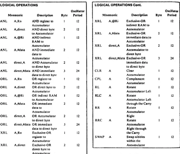
LOGICAL OPERATIONS LOGICAL OPERATIONS e.ont.
Osein.tor Oscillator
Mnemonic Description Byte Period Mnemonic DescriptiOn Byte J-erlod
ANL A.Rn AND ~gister to 12 XRL A.@Ri exclusive-OR 12
i'\ccumula:tor indirect RA M to
ANL A.direct ANDdirecl byte 12 Accumulator
to Accumulator XRL A.lldala Exclusive-OR 2 12
ANL A.@Ri AND indirect 12 immediate data.to
RAMlo Accumulator
Accumu!ator XRL direct,A Exc1usive;'()R 2 12
ANL A,lIdala ANO immediate 12 Accumulator to
data
to
direct byteAccumulator XRL direct,ltdal" Exclusive-OR 24 Ai'lL direct ,A AND Accumulator 2 12 immediate data
10 direct byte to direct byte
ANL direct,ltdala AND immediate 3 24 CLR A Clear 12
data to direct byte Accumulalof
ORL A.Rn OR register to 12 CPL A Comple.ment 12
Accumulator Accumulator
ORt A,direct OR direct byte to 12 RL A Rotate 12
Accumulalor Accumulator left
ORL A,@Ri OR indirect RAM 12 RLC A Rotate 12
to Accumulator Accumulator Left
ORL A,"data OR immediate 2 12 lhrouah the Carry
dalato RR A Rotate 12
Accumulator Accumulator
ORL direct,A OR Accumulator 12 Right
to direct byte RRC A Rotate 12
ORL direct.ltdata OR immediate 24 Accumulator
data to direct byte Right through
XRL A,Rn Eltclusive-OR 12 the Carry
register to SWAP A Swap nibbles 12
Accumulator within the:
XRL A,direct Eltclusive-OR 2 12 A«umulalor
direct byte to Accumulator
All mnemonics copyrighted G.lnlcl Corporation !9~O
8-30
(EE~
3101
MCS
e
-51 PROGRAMMER'S ·GUIOEANO
INSTRUCTION SETTable 8~10. 8051 Instruction ·Set Summary (COntinued)
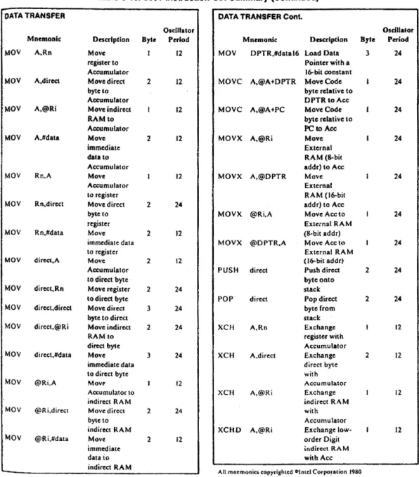
DATA TRANSFER DATA TRANSFER Conl
Oscillator Oscillator
Mnemonil: Description Byte Period Mnemonic Description Byte Period
MOY A,Rn Move [2 MOV OPTR,#data 16 Load Data 3 24
register to Pointer with a
Accumulator l6-bil constant
MOY A,direct M~vedirect 2 12 MOVC A.@A+DPTR Move Code 24
byte to byte relative to
Accumulator DPTRto Ac.c
MOY A,@Ri Move indirect 12 MOVe A.@A+PC Move Code 24
RAM eo byte relative to
Accumulator PC to Ace
MOV A,#data Move 2 12 MOVX A.@Ri Move 24
immediate External
data to RAM (8-bi(
A~umulator addr) to A~
MOV Rn,A Move 12 MOVX A.@DPTR Move 24
Accumulator External
to regisler RAM (l6-bit
MaV Rn,direct Move direct 2 24 addr) to Ace
byte [0 MOVX @Ri.A Move Aceto 24
register External RAM
MaV Rn,tI'data Move 2 12 (8-bie addr)
immediate data MOVX @DPTR.A Move Aceto 24
to register External RAM
MOV direct.A Move 2 12 (l6-bit addr)
Accumulator PUSH direct Push direct 2 24
to direct byte· byte onto
MOV direct,Rn Move register 2 24 stack
to direct byte POP direct Pop direct 2 24
MOV direct.direct Movedirecl 3 24 byte from
byte to direct staclc
Mav direcl,@Ri Move indirect 2 24 XCH A,Rn Exchange 12
RAM to register with
direct byte Accumul.ator
MaV direct.lldata Move 24 XCH A,direct Exchange 2 12
immediate data direct byte
to direct byte with
Mav @Ri.A Move- 12 Accumulator
Accumulator to XCii A,@Ri Exchange 12
indirect RA M indirect RAM
Mav @Ri.direct Move direct 2 24 with
byte to Accumulator
indirect RAM XCHO A,@Ri Exchange low- 12
~av @Ri,tI'dala Move 2 12 order Digit
immediate indirect RA M
dataio with Ace
indirect RAM
AU mnemonics c:opyrighted Olntcl Cor~rltion 1980
8-31
rEEE 370)
MCS®-S1 PROGRAMMER'S GUICE AND INSTRUCTION SET
--Table 8-10.8051 Instruction Set Summary (Continued)
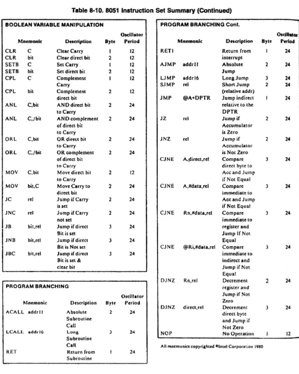
BOOLEAN VARiABLE MANIPULATION PROGRAM BRANCHING Cont.
Oscillalor Osdllator
Mnemonic Description Byte Period Mnemonic DHaiption Byte Period
CLR C Clear Carry I 12 RETI Return from 24
CLR bit Cleat direct bit 2 12 interrupt
SETS
C Set Carry I 12 AJMP addrll Absolute 2 24SETB bit Set direct bit 2 12 Jump
CPL C Complement 12 LJMP addrl6 Long Jump 24
Carry SJMP rei Short Jump 2 24
CPL bit Complement 2 12 (relative addr)
direct bit JMP @A+DPTR Jump indirect 24
ANL C.bit AND direct bit 2 24 relative to the
to Carry DPTR
ANL C./bit AND complement 2 24 JZ rei Jump if 24
of direct bit Accumulator
to Carry is Zero
ORL C,bil OR direct bil 2 24 JNZ rei Jump if 24
10 Carry Accumulator
ORL C./bit OR complement 2 24 is Notaro
of direct bit CJNE A.!1irect.re! Compare 3 24
to Carry direct byte to
MOV C,bit Move direct bit 2 12 Acc and Jump
to Carry if Not Equal
MOV bit,C Move Carry to 1 24 CJNE A.lldata.rel Compare 24
direct bit immediate to
JC rei Jump if Carry 2 24 Ace and Jump
is set if Not Equal
JNC rei Jump if Carry 2 24 CJNE Rn,#data,rel Compare 24
not set immediate to
JB bit,rel Jump if direct 24 register and
Bit is set Jump If Not
JNB bit.rel Jump ifdirecl 3 24 Equal
Bit is Not scI CJNE @Ri,lIdala.rcl Compare 24
JOC bit,re:! Jump if direct 24 immediate to
Bit is set & indirect and
clear bit Jump if Not
Equal
DJNZ Rn,rel Decrement 2 24
PROGRAM BRANCHING register and
Oscillator Jump if Not
Mnemonic Dtscrlption Bytt Period Zero
DJNZ direct,rel Decrement 24
ACALl addrll Absolute 2 24 direct byte
Subroutine and Jump if
Call Not Zero
LCALL add<l(, Long 24 NOP No Operation 12
Subroutine
Call All mnemonics copyrighled C>lntel Corporation 1990
RET Return from 24
Subroutine
APPENDIX 2
[EEE
j70i
ApPLICATION NOTES
AVAILABLE
AN3 •
AN7· ANa • AN15 • AN16· AN25 • AN29 • AN30 • AN35 • AN36 • AN39 • AN56 • AN69256 Bit
X24C44
16x16Bit
Serial Nonvolatile Static RAM
FEATURES
• Advanced CMOS Version of Xicor's X2444 • 16 x 16 Organization
• Single 5 Volt Supply
• Ideal for use with Single Chip Microcomputers -Static Timing
-MinimumUO Interface
-Serial Port.
Compatible
(COPSTM. a051)-Easity Interfaced to MicrocontroUer Ports
~ Software and Hardware Control of Nonvolatile Functions
• Auto Recall on Power-Up
• TTL and CMOS Compatible • Low Power Dissipation
-Active Current: 10mA Maximum -Standby Current: 50~ Maximum • a-Pin Mini-DIP and a-Lead sOle Packages • High Reliability
-Store Cycles: 1,000,000 -Data Retention: 100 Years
FUNCTIONAL DIAGRAM
CE(1) 01(3) . SK(2) ROW DECODE~ I, • t'&dema<l< 01 Nal~1 Semiconduelor Corp.
DESCRIPTION
The Xicor X24C44 is a serial 256 bit NOVRAM featuring a static RAM configu red 16 x 16, ove rlaid bit -by-bit with a nonvolatile E2PROM array. The X24C44 is fabricated with Xicor's Advanced CMOS Floating Gate technology. The Xicor NOVRAM design allows d~ta to be transferred between the two memory-arrays by (T1eans of software commands or external hardware inputs. A store opera-tion (RAM data to E2PROM) is completed in 5ms or less and a recall operation (E2PROM data to RAM) is com-pleted in 2~s or less.
Xicor NOVRAMs are designed for unlimited write opera-tions to
RAM.
either from the host or recalls fromE2PROM and a minimum 1,000.000 store operations. Inherent data retention is specified to be greater than
100 years. . STATIC RAM 256·81T RECAtI(6) STORE (7) 00(4) 3832 FHO FOI 2-1
383
X24C44
PIN DESCRIPTIONS Chip Enable (CE)
The Chip Enable input must be HIGH to enable all readl
write operations. CE must remain HIGH following a Read or Write command until the data transfer is com-plete. CE LOW places the X24C44 in the low power standby mode and resets the Instruction register. There· fore, CE must be brought LOW after the completion of an operation in order to reset the instruction register in preparation for the next ~ommand.
Serial Clock (SK)
The Serial Clock Input is used to clock all data into and
out of the device.
Data In (01)
Data In is the serial data input.
Data Out (00)
Data Out is the serial data output. It is in the high
impedance state except during data output cycles in
response to a READ Instruction. ~
ST'ORE
LOW will initiate an internal transfer of data fromRAM to theE2PROM array.
RECALL
RECALL
LOW will initiate an internal transfer of data from E2PROM to the RAM array.PIN CONFIGURATION CE SI( Ol 00 PIN NAMES Symbol CE SK DI DO
RE
.
CALl
STORE-
-Vee
Vss
DIP/SOle-[EEE 370J
VCCSTORe
RECAlLVss
3832 FHO F02. I Description Chip Enable Serial Clock Serial Data In Serial Data Out Recall Input Store Input+5V
Ground
X24C44
DEVICE OPERATION
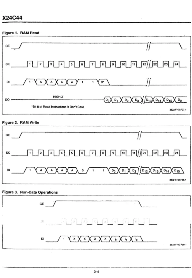
The X24C44 contains an a·bit instruction register. It is accessed via the 01 input, with data being clocked in on the rising edge of SK. CE must be HIGH during the entire data transfer operation.
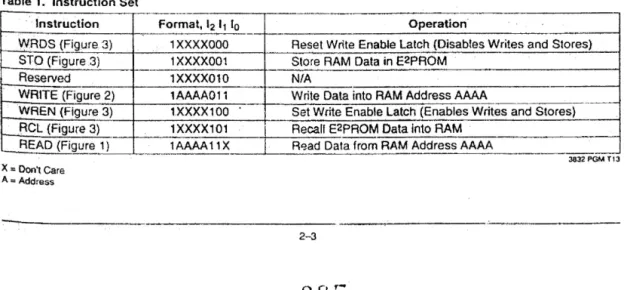
Table 1. contains a list of the instructions and their
, operation cod~s. The most significant bit (MSB) of all Instructions is a logic one (HIGH), bits 6 through 3 are either RAM address bits (A) Of don't cares (X) and bits
2 through 0 are the operation codes. The X24C44 requires the instruction to be shifted in with the MSB first. After CE is HIGH,the X24C44 will not begin to interpret the data stream until a.logic "1" has been shifted in on 01.
Therefore, CE may be brought HIGH with SK running and 01 LOW. 01 must then go HIGH to indicate the start condition of an instruction before the X24C44 will begin any action.
In addition, the SK clock is totally static. The user can completely stop the clock and data shifting wilt be stopped. Restarting the clock will resume shifting of data. RCL and RECALL
Either a software RCL instruction or a LOW on the
~ALL input will initiate a transfer of E2PROM data
into RAM. This software or hardware recall operation sets an internal "previous recaU"latch. This latch is reset upon power·up and must be intentionally set by the user to enaple any write or store operations. Although
a
recall operation is performed upon power-up. the previous recall latch isnot set by this operation.WRDS and WREN
Internally the X24C44 contains a "write enable" latch. This latch must be set for either writes to the RAM or store Table 1. Instruction Set
Instruction Format, 12 11 10
-.- -,
[EEE 170J
operations to the E2PRDM. The WREN instruction sets the latch and the WADS instruction resets the latch. disabling both
RAM
writes and E2PAOM stores, effec-tively protecting the nonvolatile data from corruption. The write enable latch Is automatically reset on power~p. STO and STOREEither the software STO instruction or a LOW on the STORE Input will initiate a transfer of data from RAM to E2PROM. In order to safeguard against unwanted store operations. the following conditions must be true: • STO instru~tion issued or STORE input is LOW. • The Inlermi'''write enable" latch must be set
(WREN instruction issued).
• The "previous recall" latch must be set (either a software or hardware recall operation).
Once the store cycle is initiated,all other device func-tions are inhibited. Upon completion ofthe store cycle, the write enable latch is reset. Refer to Figure 4 for a state diagram description of enabling/disabling condi-tions for store operacondi-tions.
WRITE
The WRITE instruction contains the 4-bit address of ,the word to be written. The write instruction is immediately followed by the 16-bit word to be written. CE must remain HIGH during the entire operation. CE must 90 LOW before the next rising edge of SK. If CE is brought LOW prematurely (after the instruction but before 16 bits of data are transferred). the instruction register will be reset and the data that was shifted-in will be written to RAM. If CE is kept HIGH for more than 24 SK clock cycles (a-bit instruction plus 16·bit data), the data alreadyshlfted-in will be overwritten.
Operation'
WRDS (Figure 3) 1XXXXOOO Reset Write Enable Latch (Disables Writes and Stores) STO (Figure 3) Reserved WRITE (Figure 2) WREN (Figure 3) RCL (Figure 3) READ (Figure 1) X:: Don't Care A= Address 1XXXXOO1 1XXXX01O 1AAAA011 tXXXX100 1 XXXX101 lAAAA11X
-Store RAM Data in E2PAOM N/A
Write Data into RAM Address AAAA
~~ Set Write Enable Latch (Enables Writ.es and Stores)
Recall E2PAOM Data into RAM Rl3ad Data from RAM Address AAAA
3832 PGM TIl
2-3
X24C44
READThe READ instruction contains the 4-bit address of the word to be accessed. Unlike the other six instructions,
'0
ofthe instruction word isa "don'teare-:This provides two advantages. Ina design. that ties both 01 and DO together. the absence of an eighth bit in ~he Instruction allows the host time to convert an 1/0 line troman output to an. input. Secondly, it allows for valid data output during the ninth SK clock cycle.qo,
the first bit output during a read operation. is trun-cated. That is, it Is internally clocked by the falling edge of the eighth SK clock; whereas. all succeeding bits are clocked by the rising edge of SK (refer to Read Cycle Diagram).LOW POWER MODE
When C.E is LOW. non-critical internal devices are powered-down. placing the device in the standby power mode, thereby minimizing power consumption. SLEEP
Because the X24C44
is
a low power CMOS device, the SLEEP instruction implemented on the first generation NMOS device has been deleted. For systems convert-ing from the X2444 to the X24C44 the software need notbe changed; the instruction will be ignored; WRITE PROTECTION
The X24C44 provides two software write protection mechanisms to prevent inadvertentstores 6funknown data.
Power-Up Condition
Upon power~up the "write enable" latch is in the reset state, disabling any store operation.
Unknown Data Store
The "previous recall" latch must be set after power-up. It may be set only by performing a software or hardware recall operation, which assures that data in all RAM locations is valid.
~---SYSTEM CONS1DERATIONS Power-Up Recall
[EEE 370]
. The X24C44 performs a power-up recall that transfers the E2PROM contents to the
RAM
array. Although the data may be read from the RAM array, tbis recall does not set the "previous recaU"'atch. During this power-up recall operation. aI/ commands are ignored. Therefore, the host should delay any operations with the X24C44 a minimumof
tpuR afterVee is stable.
Power-Down
DataProtection
Because the X24C44 is a 5V only nonvolatile memory device it may
be
susceptible to inadvertent stores to the E2PROM array during power-down cycles. Power-up cycles are not a problem b~cause the "previous recall" latch and ."write enable~ iatch. are reset. pre'ventlng any possible corruption Qf E2PROM data.Software Power-Down Protection
It the STORE and
RECALL
pins are tied toVee
through a pull-up reSistor and only software operations are performed to initiate stores, there is little likelihood of an inadvertent store. However, if these two tines are under microprocessor control, positive action should be em-ployed to negate the possibility of these control lines bouncing and generating an unwanted store. The safest method is to issue the WADS command after a write sequence and also following store operations. Note: an internal store may take up to 5ms; therefore,: the host microprocessor should delay 5ms after initiating the store prior to issuing the WADS' command ..Hardware Power-Down Protection
(when the "write enable" latch and "previous
recall" latch
are not in the reset state): . .. Holding either AECALL LOW, CE LOW:or STORE HIGH during power-down will prevent an inadvertent store.[EEE 370J
X24C44
Figure 1. RAM Read
C E . J
II
SKr
~--~---~J~---01 HIGHZ ~~ OO---~~OBit 8 of Read InstructiOns Is Don't Care
3832 FHD F07.1
Figure 2. RAM Write
CE~
II
SK
DI
3832 FHO FOe. ,
Figure 3. Non-Data Operations
I
CE~r---~\
l
DI2-5