ULN2002A . . . N PACKAGE ULN2003A . . . D, N, NS, OR PW PACKAGE
ULN2004A . . . D, N, OR NS PACKAGE ULQ2003A, ULQ2004A . . . D OR N PACKAGE
(TOP VIEW)
HIGH-VOLTAGE, HIGH-CURRENT DARLINGTON TRANSISTOR ARRAYS
Check for Samples:ULN2002A,ULN2003A,ULN2003AI,ULN2004A,ULQ2003A,ULQ2004A
1
FEATURES
•
500-mA-Rated Collector Current (Single
Output)
•
High-Voltage Outputs: 50 V
•
Output Clamp Diodes
•
Inputs Compatible With Various Types of
Logic
•
Relay-Driver Applications
DESCRIPTION
The ULN2002A, ULN2003A, ULN2003AI, ULN2004A, ULQ2003A, and ULQ2004A are high-voltage high-current
Darlington transistor arrays. Each consists of seven npn Darlington pairs that feature high-voltage outputs with
common-cathode clamp diodes for switching inductive loads. The collector-current rating of a single Darlington
pair is 500 mA. The Darlington pairs can be paralleled for higher current capability. Applications include relay
drivers, hammer drivers, lamp drivers, display drivers (LED and gas discharge), line drivers, and logic buffers.
For 100-V (otherwise interchangeable) versions of the ULN2003A and ULN2004A, see the
SN75468
and
SN75469
, respectively.
6C
ORDERING INFORMATION
(1)TA PACKAGE(2) ORDERABLE PART NUMBER TOP-SIDE MARKING
ULN2002AN ULN2002AN
PDIP – N Tube of 25 ULN2003AN ULN2003AN
ULN2004AN ULN2004AN
Tube of 40 ULN2003AD
Reel of 2500 ULN2003ADR ULN2003A
SOIC – D Reel of 2500 ULN2003ADRG3 –20°C to 70°C
Tube of 40 ULN2004AD
ULN2004A Reel of 2500 ULN2004ADRG3
ULN2003ANSR ULN2003A
SOP – NS Reel of 2000
ULN2004ANSR ULN2004A
Tube of 90 ULN2003APW
TSSOP – PW UN2003A
Reel of 2000 ULN2003APWR
ULQ2003AN ULQ2003A
PDIP – N Tube of 25
ULQ2004AN ULQ2004AN
Tube of 40 ULQ2003AD
–40°C to 85°C ULQ2003A
Reel of 2500 ULQ2003ADR SOIC – D
Tube of 40 ULQ2004AD
ULQ2004A Reel of 2500 ULQ2004ADR
SOP – NS Reel of 2000 ULN2003AINSR ULN2003AI
PDIP – N Tube of 425 ULN2003AIN ULN2003AIN
–40°C to 105°C Tube of 40 ULN2003AID
SOIC – D ULN2003AI
Reel of 2500 ULN2003AIDR
TSSOP – PW Reel of 2500 ULN2003AIPWR UN2003AI
(1) For the most current package and ordering information, see the Package Option Addendum at the end of this document, or see the TI web site atwww.ti.com.
(2) Package drawings, thermal data, and symbolization are available atwww.ti.com/packaging.
7.2 kW
3 kW 10.5 kW
ULN2002A
ULN/ULQ2003A: RB= 2.7 kW
ULN/ULQ2004A: RB= 10.5 kW
ULN2003AI: RB= 2.7 kW 7.2 kW 3 kW
ULN2003A,ULN2003AI,ULN2004A, ULQ2003A, ULQ2004A RB
SCHEMATICS (EACH DARLINGTON PAIR)
All resistor values shown are nominal.
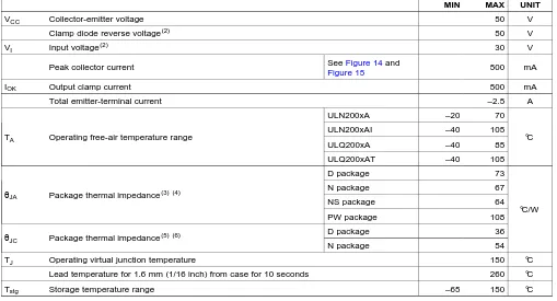
ABSOLUTE MAXIMUM RATINGS
(1) at 25°C free-air temperature (unless otherwise noted)MIN MAX UNIT
VCC Collector-emitter voltage 50 V
Clamp diode reverse voltage(2) 50 V
VI Input voltage(2) 30 V
SeeFigure 14and
Peak collector current Figure 15 500 mA
IOK Output clamp current 500 mA
Total emitter-terminal current –2.5 A
ULN200xA –20 70
ULN200xAI –40 105
TA Operating free-air temperature range °C
ULQ200xA –40 85
ULQ200xAT –40 105
D package 73
N package 67
θJA Package thermal impedance(3) (4)
NS package 64
°C/W
PW package 108
D package 36
θJC Package thermal impedance(5) (6)
N package 54
TJ Operating virtual junction temperature 150 °C
Lead temperature for 1.6 mm (1/16 inch) from case for 10 seconds 260 °C
Tstg Storage temperature range –65 150 °C
(1) Stresses beyond those listed under "absolute maximum ratings" may cause permanent damage to the device. These are stress ratings only, and functional operation of the device at these or any other conditions beyond those indicated under "recommended operating conditions" is not implied. Exposure to absolute-maximum-rated conditions for extended periods may affect device reliability. (2) All voltage values are with respect to the emitter/substrate terminal E, unless otherwise noted.
(3) Maximum power dissipation is a function of TJ(max),θJA, and TA. The maximum allowable power dissipation at any allowable ambient temperature is PD= (TJ(max) – TA)/θJA. Operating at the absolute maximum TJof 150°C can affect reliability.
(4) The package thermal impedance is calculated in accordance with JESD 51-7.
(5) Maximum power dissipation is a function of TJ(max),θJC, and TA. The maximum allowable power dissipation at any allowable ambient temperature is PD= (TJ(max) – TA)/θJC. Operating at the absolute maximum TJof 150°C can affect reliability.
(6) The package thermal impedance is calculated in accordance with MIL-STD-883.
ELECTRICAL CHARACTERISTICS
TA= 25°CULN2002A TEST
PARAMETER TEST CONDITIONS UNIT
FIGURE MIN TYP MAX
VI(on) On-state input voltage Figure 6 VCE= 2 V, IC= 300 mA 13 V
II= 250μA, IC= 100 mA 0.9 1.1
VCE(sat) Collector-emitter saturation voltage Figure 4 II= 350μA, IC= 200 mA 1 1.3 V
ELECTRICAL CHARACTERISTICS
TA= 25°CULN2003A ULN2004A
TEST
PARAMETER TEST CONDITIONS UNIT
FIGURE MIN TYP MAX MIN TYP MAX
IC= 125 mA 5
II(off) Off-state input current Figure 3 T 50 65 50 65 μA
A= 70°C,
PARAMETER TEST FIGURE UNIT
CONDITIONS MIN TYP MAX
IC= 200 mA 2.4
VI(on) On-state input voltage Figure 6 VCE= 2 V IC= 250 mA 2.7 V
IC= 300 mA 3
II= 250μA, IC= 100 mA 0.9 1.1
VCE(sat) Collector-emitter saturation voltage Figure 5 II= 350μA, IC= 200 mA 1 1.3 V
ELECTRICAL CHARACTERISTICS
TA= –40°C to 105°CULN2003AI
PARAMETER TEST FIGURE TEST CONDITIONS UNIT
MIN TYP MAX
IC= 200 mA 2.7
VI(on) On-state input voltage Figure 6 VCE= 2 V IC= 250 mA 2.9 V
IC= 300 mA 3
II= 250μA, IC= 100 mA 0.9 1.2
VCE(sat) Collector-emitter saturation voltage Figure 5 II= 350μA, IC= 200 mA 1 1.4 V
II= 500μA, IC= 350 mA 1.2 1.7
over recommended operating conditions (unless otherwise noted)
ULQ2003A ULQ2004A
TEST
PARAMETER TEST CONDITIONS UNIT
FIGURE MIN TYP MAX MIN TYP MAX
SWITCHING CHARACTERISTICS
TA= 25°CULN2002A, ULN2003A, ULN2004A
PARAMETER TEST CONDITIONS UNIT
MIN TYP MAX
tPLH Propagation delay time, low- to high-level output SeeFigure 9 0.25 1 μs
tPHL Propagation delay time, high- to low-level output SeeFigure 9 0.25 1 μs
VOH High-level output voltage after switching VS= 50 V, IO= 300 mA, SeeFigure 10 VS – 20 mV
SWITCHING CHARACTERISTICS
TA= 25°CULN2003AI
PARAMETER TEST CONDITIONS UNIT
MIN TYP MAX
tPLH Propagation delay time, low- to high-level output SeeFigure 9 0.25 1 μs
tPHL Propagation delay time, high- to low-level output SeeFigure 9 0.25 1 μs
VOH High-level output voltage after switching VS= 50 V, IO≈300 mA, SeeFigure 10 VS – 20 mV
SWITCHING CHARACTERISTICS
TA= –40°C to 105°CULN2003AI
PARAMETER TEST CONDITIONS UNIT
MIN TYP MAX
tPLH Propagation delay time, low- to high-level output SeeFigure 9 1 10 μs
tPHL Propagation delay time, high- to low-level output SeeFigure 9 1 10 μs
VOH High-level output voltage after switching VS= 50 V, IO≈300 mA, SeeFigure 10 VS – 50 mV
SWITCHING CHARACTERISTICS
over recommended operating conditions (unless otherwise noted)
ULQ2003A, ULQ2004A
PARAMETER TEST CONDITIONS UNIT
MIN TYP MAX
tPLH Propagation delay time, low- to high-level output SeeFigure 9 1 10 μs
tPHL Propagation delay time, high- to low-level output SeeFigure 9 1 10 μs
VR
Open
IR VF IF
Open Open
VCE IC
II
hFE = ICII
Open
VCE IC
VI(on) Open VCE
IC II(off)
Open
Open II(on)
VI Open
VCE
Open
ICEX
Open
VCE
VI
ICEX
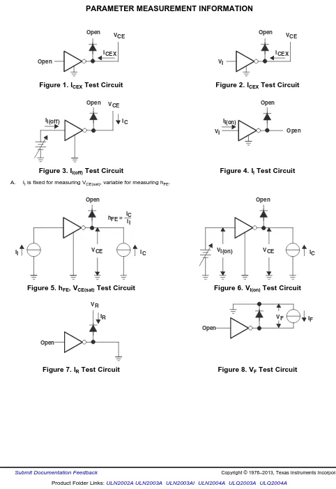
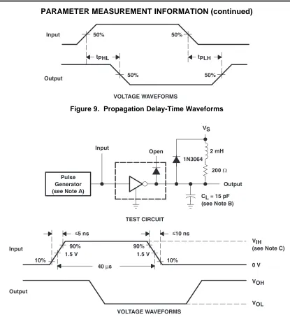
PARAMETER MEASUREMENT INFORMATION
Figure 1. I
CEXTest Circuit
Figure 2. I
CEXTest Circuit
Figure 3. I
I(off)Test Circuit
Figure 4. I
ITest Circuit
A. IIis fixed for measuring VCE(sat), variable for measuring hFE.
Figure 5. h
FE, V
CE(sat)Test Circuit
Figure 6. V
I(on)Test Circuit
90% 90%
1.5 V 1.5 V
10% 10%
40µs
≤10 ns ≤5 ns
VIH (see Note C)
0 V
VOH
VOL Input
Output
VOLTAGE WAVEFORMS
200W
PARAMETER MEASUREMENT INFORMATION (continued)
Figure 9. Propagation Delay-Time Waveforms
A. The pulse generator has the following characteristics: PRR = 12.5 kHz, ZO= 50Ω.
B. CLincludes probe and jig capacitance.
C. For testing the ULN2003A, ULN2003AI, and ULQ2003A, VIH= 3 V; for the ULN2002A, VIH= 13 V; for the ULN2004A and the ULQ2004A, VIH= 8 V.
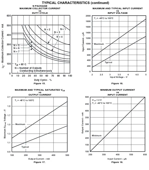
0
N = Number of Outputs Conducting Simultaneously
IC(tot) - Total Collector Current - mA 0
IC - Collector Current - mA 2.5
800 0
100 200 300 400 500 600 700 0.5
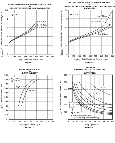
COLLECTOR-EMITTER SATURATION VOLTAGE
COLLECTOR-EMITTER SATURATION VOLTAGE vs
vs TOTAL COLLECTOR CURRENT (TWO DARLINGTONS IN
COLLECTOR CURRENT (ONE DARLINGTON) PARALLEL)
Figure 11. Figure 12.
D PACKAGE
COLLECTOR CURRENT MAXIMUM COLLECTOR CURRENT
vs vs
INPUT CURRENT DUTY CYCLE
0.9
100 200 300 400 500
Output Current – mA
Maxim
250 350 450 550 650
Input Current – µA
Output Current N = Number of Outputs 500
Input Voltage – V
Input Current – µA
TJ= -40°C to 105°C
Maximum
Typical
TYPICAL CHARACTERISTICS (continued)
N PACKAGEMAXIMUM COLLECTOR CURRENT MAXIMUM AND TYPICAL INPUT CURRENT
vs vs
DUTY CYCLE INPUT VOLTAGE
Figure 15. Figure 16.
MAXIMUM AND TYPICAL SATURATED VCE MINIMUM OUTPUT CURRENT
vs vs
OUTPUT CURRENT INPUT CURRENT
VCC V
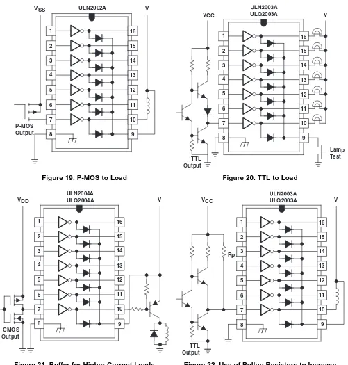
Figure 19. P-MOS to Load
Figure 20. TTL to Load
REVISION HISTORY
Changes from Revision K (August 2011) to Revision L Page
• Removed reference to obsolete ULN2001 part ... 1
Changes from Revision L (March 2012) to Revision M Page
PACKAGING INFORMATION
Orderable Device Status
(1)
Package Type Package Drawing
MSL Peak Temp (3)
Op Temp (°C) Device Marking
(4/5)
Samples
ULN2001AD OBSOLETE SOIC D 16 TBD Call TI Call TI
ULN2001ADR OBSOLETE SOIC D 16 TBD Call TI Call TI
ULN2001AN OBSOLETE PDIP N 16 TBD Call TI Call TI
ULN2002AD OBSOLETE SOIC D 16 TBD Call TI Call TI
ULN2002AN ACTIVE PDIP N 16 25 Pb-Free
(RoHS)
CU NIPDAU N / A for Pkg Type -20 to 70 ULN2002AN
ULN2002ANE4 ACTIVE PDIP N 16 25 Pb-Free
(RoHS)
CU NIPDAU N / A for Pkg Type -20 to 70 ULN2002AN
ULN2003AD ACTIVE SOIC D 16 40 Green (RoHS
& no Sb/Br)
CU NIPDAU Level-1-260C-UNLIM -20 to 70 ULN2003A
ULN2003ADE4 ACTIVE SOIC D 16 40 Green (RoHS
& no Sb/Br)
CU NIPDAU Level-1-260C-UNLIM -20 to 70 ULN2003A
ULN2003ADG4 ACTIVE SOIC D 16 40 Green (RoHS
& no Sb/Br)
CU NIPDAU Level-1-260C-UNLIM -20 to 70 ULN2003A
ULN2003ADR ACTIVE SOIC D 16 2500 Green (RoHS
& no Sb/Br)
CU NIPDAU | CU SN Level-1-260C-UNLIM -20 to 70 ULN2003A
ULN2003ADRE4 ACTIVE SOIC D 16 2500 Green (RoHS
& no Sb/Br)
CU NIPDAU Level-1-260C-UNLIM -20 to 70 ULN2003A
ULN2003ADRG3 ACTIVE SOIC D 16 2500 Green (RoHS
& no Sb/Br)
CU SN Level-1-260C-UNLIM -20 to 70 ULN2003A
ULN2003ADRG4 ACTIVE SOIC D 16 2500 Green (RoHS
& no Sb/Br)
CU NIPDAU Level-1-260C-UNLIM -20 to 70 ULN2003A
ULN2003AID ACTIVE SOIC D 16 40 Green (RoHS
& no Sb/Br)
CU NIPDAU Level-1-260C-UNLIM -40 to 105 ULN2003AI
ULN2003AIDE4 ACTIVE SOIC D 16 40 Green (RoHS
& no Sb/Br)
CU NIPDAU Level-1-260C-UNLIM -40 to 105 ULN2003AI
Orderable Device Status
(1)
Package Type Package Drawing
MSL Peak Temp
(3)
Op Temp (°C) Device Marking
(4/5)
Samples
ULN2003AIN ACTIVE PDIP N 16 25 Pb-Free
(RoHS)
CU NIPDAU N / A for Pkg Type -40 to 105 ULN2003AIN
ULN2003AINE4 ACTIVE PDIP N 16 25 Pb-Free
(RoHS)
CU NIPDAU N / A for Pkg Type -40 to 105 ULN2003AIN
ULN2003AINSR ACTIVE SO NS 16 2000 Green (RoHS
& no Sb/Br)
CU NIPDAU Level-1-260C-UNLIM -40 to 105 ULN2003AI
ULN2003AIPW ACTIVE TSSOP PW 16 90 Green (RoHS
& no Sb/Br)
CU NIPDAU Level-1-260C-UNLIM -40 to 105 UN2003AI
ULN2003AIPWE4 ACTIVE TSSOP PW 16 90 Green (RoHS
& no Sb/Br)
CU NIPDAU Level-1-260C-UNLIM -40 to 105 UN2003AI
ULN2003AIPWG4 ACTIVE TSSOP PW 16 90 Green (RoHS
& no Sb/Br)
CU NIPDAU Level-1-260C-UNLIM -40 to 105 UN2003AI
ULN2003AIPWR ACTIVE TSSOP PW 16 2000 Green (RoHS & no Sb/Br)
CU NIPDAU | CU SN Level-1-260C-UNLIM -40 to 105 UN2003AI
ULN2003AIPWRE4 ACTIVE TSSOP PW 16 2000 Green (RoHS & no Sb/Br)
CU NIPDAU Level-1-260C-UNLIM -40 to 105 UN2003AI
ULN2003AIPWRG4 ACTIVE TSSOP PW 16 2000 Green (RoHS & no Sb/Br)
CU NIPDAU Level-1-260C-UNLIM -40 to 105 UN2003AI
ULN2003AJ OBSOLETE CDIP J 16 TBD Call TI Call TI -55 to 125
ULN2003AN ACTIVE PDIP N 16 25 Pb-Free
(RoHS)
CU NIPDAU | CU SN N / A for Pkg Type -20 to 70 ULN2003AN
ULN2003ANE3 PREVIEW PDIP N 16 25 TBD Call TI Call TI -20 to 70
ULN2003ANE4 ACTIVE PDIP N 16 25 Pb-Free
(RoHS)
CU NIPDAU N / A for Pkg Type -20 to 70 ULN2003AN
Orderable Device Status
(1)
Package Type Package Drawing
MSL Peak Temp
(3)
Op Temp (°C) Device Marking
(4/5)
Samples
ULN2003APWR ACTIVE TSSOP PW 16 2000 Green (RoHS
& no Sb/Br)
CU NIPDAU | CU SN Level-1-260C-UNLIM -20 to 70 UN2003A
ULN2003APWRE4 ACTIVE TSSOP PW 16 2000 Green (RoHS & no Sb/Br)
CU NIPDAU Level-1-260C-UNLIM -20 to 70 UN2003A
ULN2003APWRG4 ACTIVE TSSOP PW 16 2000 Green (RoHS & no Sb/Br)
CU NIPDAU Level-1-260C-UNLIM -20 to 70 UN2003A
ULN2004AD ACTIVE SOIC D 16 40 Green (RoHS
& no Sb/Br)
CU NIPDAU Level-1-260C-UNLIM -20 to 70 ULN2004A
ULN2004ADE4 ACTIVE SOIC D 16 40 Green (RoHS
& no Sb/Br)
CU NIPDAU Level-1-260C-UNLIM -20 to 70 ULN2004A
ULN2004ADG4 ACTIVE SOIC D 16 40 Green (RoHS
& no Sb/Br)
CU NIPDAU Level-1-260C-UNLIM -20 to 70 ULN2004A
ULN2004ADR ACTIVE SOIC D 16 2500 Green (RoHS
& no Sb/Br)
CU NIPDAU | CU SN Level-1-260C-UNLIM -20 to 70 ULN2004A
ULN2004ADRE4 ACTIVE SOIC D 16 2500 Green (RoHS
& no Sb/Br)
CU NIPDAU Level-1-260C-UNLIM -20 to 70 ULN2004A
ULN2004ADRG4 ACTIVE SOIC D 16 2500 Green (RoHS
& no Sb/Br)
CU NIPDAU Level-1-260C-UNLIM -20 to 70 ULN2004A
ULN2004AN ACTIVE PDIP N 16 25 Pb-Free
(RoHS)
CU NIPDAU N / A for Pkg Type -20 to 70 ULN2004AN
ULN2004ANE4 ACTIVE PDIP N 16 25 Pb-Free
(RoHS)
CU NIPDAU N / A for Pkg Type -20 to 70 ULN2004AN
ULN2004ANSR ACTIVE SO NS 16 2000 Green (RoHS
& no Sb/Br)
CU NIPDAU Level-1-260C-UNLIM -20 to 70 ULN2004A
ULN2004ANSRG4 ACTIVE SO NS 16 2000 Green (RoHS
& no Sb/Br)
CU NIPDAU Level-1-260C-UNLIM -20 to 70 ULN2004A
ULQ2003AD ACTIVE SOIC D 16 40 Green (RoHS
& no Sb/Br)
CU NIPDAU Level-1-260C-UNLIM -40 to 85 ULQ2003A
Orderable Device Status
(1)
Package Type Package Drawing
MSL Peak Temp
(3)
Op Temp (°C) Device Marking
(4/5)
Samples
ULQ2004AD ACTIVE SOIC D 16 40 Green (RoHS
& no Sb/Br)
CU NIPDAU Level-1-260C-UNLIM -40 to 85 ULQ2004A
ULQ2004ADG4 ACTIVE SOIC D 16 40 Green (RoHS
& no Sb/Br)
CU NIPDAU Level-1-260C-UNLIM ULQ2004A
ULQ2004ADR ACTIVE SOIC D 16 2500 Green (RoHS
& no Sb/Br)
CU NIPDAU Level-1-260C-UNLIM -40 to 85 ULQ2004A
ULQ2004ADRG4 ACTIVE SOIC D 16 2500 Green (RoHS
& no Sb/Br)
CU NIPDAU Level-1-260C-UNLIM ULQ2004A
ULQ2004AN ACTIVE PDIP N 16 25 Pb-Free
(RoHS)
CU NIPDAU N / A for Pkg Type -40 to 85 ULQ2004AN
(1)
The marketing status values are defined as follows:
ACTIVE: Product device recommended for new designs.
LIFEBUY: TI has announced that the device will be discontinued, and a lifetime-buy period is in effect.
NRND: Not recommended for new designs. Device is in production to support existing customers, but TI does not recommend using this part in a new design. PREVIEW: Device has been announced but is not in production. Samples may or may not be available.
OBSOLETE: TI has discontinued the production of the device.
(2)
Eco Plan - The planned eco-friendly classification: Pb-Free (RoHS), Pb-Free (RoHS Exempt), or Green (RoHS & no Sb/Br) - please check http://www.ti.com/productcontent for the latest availability information and additional product content details.
TBD: The Pb-Free/Green conversion plan has not been defined.
Pb-Free (RoHS): TI's terms "Lead-Free" or "Pb-Free" mean semiconductor products that are compatible with the current RoHS requirements for all 6 substances, including the requirement that
lead not exceed 0.1% by weight in homogeneous materials. Where designed to be soldered at high temperatures, TI Pb-Free products are suitable for use in specified lead-free processes.
Pb-Free (RoHS Exempt): This component has a RoHS exemption for either 1) lead-based flip-chip solder bumps used between the die and package, or 2) lead-based die adhesive used between
the die and leadframe. The component is otherwise considered Pb-Free (RoHS compatible) as defined above.
Green (RoHS & no Sb/Br): TI defines "Green" to mean Pb-Free (RoHS compatible), and free of Bromine (Br) and Antimony (Sb) based flame retardants (Br or Sb do not exceed 0.1% by weight
Important Information and Disclaimer:The information provided on this page represents TI's knowledge and belief as of the date that it is provided. TI bases its knowledge and belief on information
provided by third parties, and makes no representation or warranty as to the accuracy of such information. Efforts are underway to better integrate information from third parties. TI has taken and continues to take reasonable steps to provide representative and accurate information but may not have conducted destructive testing or chemical analysis on incoming materials and chemicals. TI and TI suppliers consider certain information to be proprietary, and thus CAS numbers and other limited information may not be available for release.
In no event shall TI's liability arising out of such information exceed the total purchase price of the TI part(s) at issue in this document sold by TI to Customer on an annual basis.
OTHER QUALIFIED VERSIONS OF ULQ2003A, ULQ2004A :
•
Automotive: ULQ2003A-Q1, ULQ2004A-Q1NOTE: Qualified Version Definitions:
TAPE AND REEL INFORMATION
*All dimensions are nominal
Device Package
Type
Package Drawing
Pins SPQ Reel
Diameter (mm)
Reel Width W1 (mm)
A0 (mm)
B0 (mm)
K0 (mm)
P1 (mm)
W (mm)
Pin1 Quadrant
ULN2003ADR SOIC D 16 2500 330.0 16.8 6.5 10.3 2.1 8.0 16.0 Q1
ULN2003ADR SOIC D 16 2500 330.0 16.4 6.5 10.3 2.1 8.0 16.0 Q1
ULN2003ADRG3 SOIC D 16 2500 330.0 16.8 6.5 10.3 2.1 8.0 16.0 Q1
ULN2003ADRG4 SOIC D 16 2500 330.0 16.4 6.5 10.3 2.1 8.0 16.0 Q1
ULN2003AIDR SOIC D 16 2500 330.0 16.8 6.5 10.3 2.1 8.0 16.0 Q1
ULN2003AIDR SOIC D 16 2500 330.0 16.4 6.5 10.3 2.1 8.0 16.0 Q1
ULN2003AIDRG4 SOIC D 16 2500 330.0 16.4 6.5 10.3 2.1 8.0 16.0 Q1
ULN2003AIPWR TSSOP PW 16 2000 330.0 12.4 6.9 5.6 1.6 8.0 12.0 Q1
ULN2003AIPWR TSSOP PW 16 2000 330.0 12.4 7.0 5.6 1.6 8.0 12.0 Q1
ULN2003AIPWRG4 TSSOP PW 16 2000 330.0 12.4 6.9 5.6 1.6 8.0 12.0 Q1
ULN2003APWR TSSOP PW 16 2000 330.0 12.4 6.9 5.6 1.6 8.0 12.0 Q1
Device Package Type
Package Drawing
Pins SPQ Reel
Diameter (mm)
Reel Width W1 (mm)
A0 (mm)
B0 (mm)
K0 (mm)
P1 (mm)
W (mm)
Pin1 Quadrant
ULQ2003ADR SOIC D 16 2500 330.0 16.4 6.5 10.3 2.1 8.0 16.0 Q1
*All dimensions are nominal
Device Package Type Package Drawing Pins SPQ Length (mm) Width (mm) Height (mm)
ULN2003ADR SOIC D 16 2500 364.0 364.0 27.0
ULN2003ADR SOIC D 16 2500 333.2 345.9 28.6
ULN2003ADRG3 SOIC D 16 2500 364.0 364.0 27.0
ULN2003ADRG4 SOIC D 16 2500 333.2 345.9 28.6
ULN2003AIDR SOIC D 16 2500 364.0 364.0 27.0
ULN2003AIDR SOIC D 16 2500 333.2 345.9 28.6
ULN2003AIDRG4 SOIC D 16 2500 333.2 345.9 28.6
ULN2003AIPWR TSSOP PW 16 2000 367.0 367.0 35.0
ULN2003AIPWR TSSOP PW 16 2000 364.0 364.0 27.0
ULN2003AIPWRG4 TSSOP PW 16 2000 367.0 367.0 35.0
ULN2003APWR TSSOP PW 16 2000 367.0 367.0 35.0
ULN2003APWR TSSOP PW 16 2000 364.0 364.0 27.0
Device Package Type Package Drawing Pins SPQ Length (mm) Width (mm) Height (mm)
ULN2004ADRG4 SOIC D 16 2500 367.0 367.0 38.0
ULN2004ADRG4 SOIC D 16 2500 333.2 345.9 28.6
TI warrants performance of its components to the specifications applicable at the time of sale, in accordance with the warranty in TI’s terms and conditions of sale of semiconductor products. Testing and other quality control techniques are used to the extent TI deems necessary to support this warranty. Except where mandated by applicable law, testing of all parameters of each component is not necessarily performed.
TI assumes no liability for applications assistance or the design of Buyers’ products. Buyers are responsible for their products and applications using TI components. To minimize the risks associated with Buyers’ products and applications, Buyers should provide adequate design and operating safeguards.
TI does not warrant or represent that any license, either express or implied, is granted under any patent right, copyright, mask work right, or other intellectual property right relating to any combination, machine, or process in which TI components or services are used. Information published by TI regarding third-party products or services does not constitute a license to use such products or services or a warranty or endorsement thereof. Use of such information may require a license from a third party under the patents or other intellectual property of the third party, or a license from TI under the patents or other intellectual property of TI.
Reproduction of significant portions of TI information in TI data books or data sheets is permissible only if reproduction is without alteration and is accompanied by all associated warranties, conditions, limitations, and notices. TI is not responsible or liable for such altered documentation. Information of third parties may be subject to additional restrictions.
Resale of TI components or services with statements different from or beyond the parameters stated by TI for that component or service voids all express and any implied warranties for the associated TI component or service and is an unfair and deceptive business practice. TI is not responsible or liable for any such statements.
Buyer acknowledges and agrees that it is solely responsible for compliance with all legal, regulatory and safety-related requirements concerning its products, and any use of TI components in its applications, notwithstanding any applications-related information or support that may be provided by TI. Buyer represents and agrees that it has all the necessary expertise to create and implement safeguards which anticipate dangerous consequences of failures, monitor failures and their consequences, lessen the likelihood of failures that might cause harm and take appropriate remedial actions. Buyer will fully indemnify TI and its representatives against any damages arising out of the use of any TI components in safety-critical applications.
In some cases, TI components may be promoted specifically to facilitate safety-related applications. With such components, TI’s goal is to help enable customers to design and create their own end-product solutions that meet applicable functional safety standards and requirements. Nonetheless, such components are subject to these terms.
No TI components are authorized for use in FDA Class III (or similar life-critical medical equipment) unless authorized officers of the parties have executed a special agreement specifically governing such use.
Only those TI components which TI has specifically designated as military grade or “enhanced plastic” are designed and intended for use in military/aerospace applications or environments. Buyer acknowledges and agrees that any military or aerospace use of TI components which have not been so designated is solely at the Buyer's risk, and that Buyer is solely responsible for compliance with all legal and regulatory requirements in connection with such use.
TI has specifically designated certain components as meeting ISO/TS16949 requirements, mainly for automotive use. In any case of use of non-designated products, TI will not be responsible for any failure to meet ISO/TS16949.
Products Applications
Audio www.ti.com/audio Automotive and Transportation www.ti.com/automotive Amplifiers amplifier.ti.com Communications and Telecom www.ti.com/communications
Data Converters dataconverter.ti.com Computers and Peripherals www.ti.com/computers
DLP® Products www.dlp.com Consumer Electronics www.ti.com/consumer-apps
DSP dsp.ti.com Energy and Lighting www.ti.com/energy
Clocks and Timers www.ti.com/clocks Industrial www.ti.com/industrial
Interface interface.ti.com Medical www.ti.com/medical
Logic logic.ti.com Security www.ti.com/security