The following topics are addressed in this section:
1.1 Scope... 1-2 1.2 Purpose ... 1-3 1.3 Personnel Proficiency... 1-3 1.4 Classification... 1-3
1.5 Definition of Requirements ... 1-3 1.5.1 Acceptance Criteria ... 1-4 1.5.1.1 Target Condition ... 1-4 1.5.1.2 Acceptable Condition ... 1-4 1.5.1.3 Defect Condition ... 1-4 1.5.1.3.1 Disposition ... 1-4 1.5.1.4 Process Indicator Condition ... 1-4 1.5.1.4.1 Process Indicator Methodologies ... 1-4 1.5.1.5 Combined Conditions ... 1-4 1.5.1.6 Conditions Not Specified ... 1-5 1.5.1.7 Specialized Designs ... 1-5
1.6 Terms and Definitions... 1-5 1.6.1 Board Orientation ... 1-5 1.6.1.1 *Primary Side ... 1-5
1.6.1.2 *Secondary Side ... 1-5 1.6.1.3 *Solder Source Side ... 1-5 1.6.1.4 *Solder Destination Side ... 1-5 1.6.2 *Cold Solder Connection ... 1-5 1.6.3 Electrical Clearance ... 1-5 1.6.4 FOD (Foreign Object Debris) ... 1-5 1.6.5 High Voltage ... 1-5 1.6.6 Intrusive Solder ... 1-6 1.6.7 Meniscus (Component) ... 1-6 1.6.8 *Nonfunctional Land ... 1-6 1.6.9 Pin-in-Paste ... 1-6 1.6.10 Solder Balls ... 1-6 1.6.11 Wire Diameter ... 1-6 1.6.12 Wire Overlap ... 1-6 1.6.13 Wire Overwrap ... 1-6
1.7 Examples and Illustrations ... 1-6 1.8 Inspection Methodology ... 1-6 1.9 Verification of Dimensions ... 1-6 1.10 Magnification Aids ... 1-6 1.11 Lighting ... 1-7 1 Acceptability of Electronic Assemblies
1.1 Scope This standard is a collection of visual quality acceptability requirements for electronic assemblies. This standard does not provide criteria for cross-section evaluation.
This document presents acceptance requirements for the manufacture of electrical and electronic assemblies. Historically, elec-tronic assembly standards contained a more comprehensive tutorial addressing principles and techniques. For a more complete understanding of this document’s recommendations and requirements, one may use this document in conjunction with IPC-HDBK-001, IPC-AJ-820 and IPC J-STD-001.
The criteria in this standard are not intended to define processes to accomplish assembly operations nor is it intended to autho-rize repair/modification or change of the customer’s product. For instance, the presence of criteria for adhesive bonding of com-ponents does not imply/authorize/require the use of adhesive bonding, and the depiction of a lead wrapped clockwise around a terminal does not imply/authorize/require that all leads/wires be wrapped in the clockwise direction.
Users of this standard should be knowledgeable of the applicable requirements of the document and how to apply them. Objective evidence of the demonstration of this knowledge should be maintained. Where objective evidence is unavailable, the organization should consider periodic review of personnel skills to determine visual acceptance criteria appropriately.
IPC-A-610 has criteria outside the scope of IPC J-STD-001 defining handling, mechanical and other workmanship requirements. Table 1-1 is a summary of related documents.
Table 1-1 Summary of Related Documents
Document Purpose
Specification
Number Definition
Design Standard IPC-2220 (Series) IPC-7351 IPC-CM-770
Design requirements reflecting three levels of complexity (Levels A, B, and C) indicating finer geometries, greater densities, more process steps to produce the product.
Component and Assembly Process Guidelines to assist in the design of the bare board and the assembly where the bare board processes concentrate on land pat-terns for surface mount and the assembly concentrates on surface mount and through-hole principles which are usually incorporated into the design process and the documentation.
PCB Requirements IPC-6010 (series) IPC-A-600
Requirements and acceptance documentation for rigid, rigid flex, flex and other types of substrates.
End Item Documentation IPC-D-325 Documentation depicting bare board specific end product requirements designed by the customer or end item assembly requirements. Details may or may not refer-ence industry specifications or workmanship standards as well as customer’s own preferences or internal standard requirements.
End Item Standards IPC J-STD-001 Requirements for soldered electrical and electronic assemblies depicting minimum end product acceptable characteristics as well as methods for evaluation (test methods), frequency of testing and applicable ability of process control require-ments.
Acceptability Standard IPC-A-610 Pictorial interpretive document indicating various characteristics of the board and/or assembly as appropriate relating to desirable conditions that exceed the minimum acceptable characteristics indicated by the end item performance standard and reflect various out-of-control (process indicator or defect) conditions to assist the shop process evaluators in judging need for corrective action.
Training Programs (Optional)
Documented training requirements for teaching and learning process procedures and techniques for implementing acceptance requirements of either end item standards, acceptability standards, or requirements detailed on the customer documentation.
Rework and Repair IPC-7711/7721 Documentation providing the procedures to accomplish conformal coating and component removal and replacement, solder resist repair, and modification/repair of laminate material, conductors, and plated-through holes.
IPC-AJ-820 is a supporting document that provides information regarding the intent of this specification content and explains or amplifies the technical rationale for transition of limits through Target to Defect condition criteria. In addition, supporting informa-tion is provided to give a broader understanding of the process considerainforma-tions that are related to performance but not commonly distinguishable through visual assessment methods.
The explanations provided in IPC-AJ-820 should be useful in determining disposition of conditions identified as Defect, processes associated with Process Indicators, as well as answering questions regarding clarification in use and application for defined con-tent of this specification. Contractual reference to IPC-A-610 does not additionally impose the concon-tent of IPC-AJ-820 unless spe-cifically referenced in contractual documentation.
1.2 Purpose The visual standards in this document reflect the requirements of existing IPC and other applicable specifications. In order for the user to apply and use the content of this document, the assembly/product should comply with other existing IPC requirements, such as IPC-7351, IPC-2220 (Series), IPC-6010 (Series) and IPC-A-600. If the assembly does not comply with these or with equivalent requirements, the acceptance criteriashallbe defined between the customer and supplier.
The illustrations in this document portray specific points noted in the title of each page. A brief description follows each illustration. It is not the intent of this document to exclude any acceptable procedure for component placement or for applying flux and sol-der used to make the electrical connection; however, the methods usedshallproduce completed solder connections conform-ing to the acceptability requirements described in this document.
In the case of a discrepancy, the description or written criteria always takes precedence over the illustrations.
1.3 Personnel Proficiency All instructors, operators and all inspection personnel shallbe proficient in the tasks to be per-formed. Objective evidence of that proficiencyshall be maintained and available for review. Objective evidence should include records of training to the applicable job functions being performed, work experience, testing to the requirements of this standard, and/or results of periodic reviews of proficiency. Supervised on-the-job training is acceptable until proficiency is demonstrated.
1.4 Classification Accept and/or reject decisionsshallbe based on applicable documentation such as contracts, drawings, specifications, standards and reference documents. Criteria defined in this document reflect three classes, which are as follows:
Class 1 – General Electronic Products
Includes products suitable for applications where the major requirement is function of the completed assembly.
Class 2 – Dedicated Service Electronic Products
Includes products where continued performance and extended life is required, and for which uninterrupted service is desired but not critical. Typically the end-use environment would not cause failures.
Class 3 – High Performance/Harsh Environment Electronic Products
Includes products where continued high performance or performance-on-demand is critical, equipment downtime cannot be tol-erated, end-use environment may be uncommonly harsh, and the equipment must function when required, such as life support or other critical systems.
The customer (user) has the ultimate responsibility for identifying the class to which the assembly is evaluated. If the user and manufacturer do not establish and document the acceptance class, the manufacturer may do so.
1.5 Definition of Requirements This document provides acceptance criteria for completed electronic assemblies. Where a requirement is presented that cannot be defined by the acceptable, process indicator, and defect conditions, the word ‘‘shall‘‘ is used to identify the requirement. Unless otherwise specified herein, the word ‘‘shall‘‘ in this document invokes a requirement for manufacturers of all classes or product, and failure to comply with the requirement is a noncompliance to this standard.
All products shallmeet the requirements of the assembly drawing(s)/ documentation and the requirements for the applicable product class specified herein. Missing hardware or components are a Defect for all classes.
1 Acceptability of Electronic Assemblies
1.5.1 Acceptance Criteria When IPC-A-610 is cited or required by contract as a stand-alone document for inspection and/or acceptance, the requirements of IPC J-STD-001 ‘‘Requirements for Soldered Electrical and Electronic Assemblies’’ do not apply unless separately and specifically required.
In the event of conflict, the following order of precedence applies:
1. Procurement as agreed and documented between customer and supplier.
2. Master drawing or master assembly drawing reflecting the customer’s detailed requirements. 3. When invoked by the customer or per contractual agreement, IPC-A-610.
When documents other than IPC-A-610 are cited, the order of precedenceshallbe defined in the procurement documents. Criteria are given for each class in four conditions: Target, Acceptable, Defect or Process Indicator. ‘‘Not established’’ means that there is no specified criteria for that class and may need to be established between Manufacturer and User.
1.5.1.1 Target Condition A condition that is close to perfect/preferred, however, it is a desirable condition and not always achievable and may not be necessary to ensure reliability of the assembly in its service environment.
1.5.1.2 Acceptable Condition This characteristic indicates a condition that, while not necessarily perfect, will maintain the integrity and reliability of the assembly in its service environment.
1.5.1.3 Defect Condition A defect is a condition that may be insufficient to ensure the form, fit or function of the assembly in its end use environment. Defect conditionsshallbe dispositioned by the manufacturer based on design, service, and customer requirements. Disposition may be to rework, repair, scrap, or use as is. Repair or ‘‘use as is’’ may require customer concurrence. It is the responsibility of the User to define unique defect categories applicable to the product.
A defect for Class 1 automatically implies a defect for Class 2 and 3. A defect for Class 2 implies a defect for Class 3.
1.5.1.3.1 Disposition The determination of how defects should be treated. Dispositions include, but are not limited to, rework, use as is, scrap or repair.
1.5.1.4 Process Indicator Condition A process indicator is a condition (not a defect) that identifies a characteristic that does not affect the form, fit or function of a product.
• Such condition is a result of material, design and/or operator/machine related causes that create a condition that neither fully meets the acceptance criteria nor is a defect.
• Process indicators should be monitored as part of the process control system. When the number of process indicators indicate abnormal variation in the process or identify an undesirable trend, then the process should be analyzed. This may result in action to reduce the variation and improve yields.
• Disposition of individual process indicators is not required and affected product should be used as is.
1.5.1.4.1 Process Control Methodologies Process control methodologies are to be used in the planning, implementation and evaluation of the manufacturing processes used to produce soldered electrical and electronic assemblies. The philosophy, imple-mentation strategies, tools and techniques may be applied in different sequences depending on the specific company, operation, or variable under consideration to relate process control and capability to end product requirements. The manufacturer needs to maintain objective evidence of a current process control/continuous improvement plan that is available for review.
1.5.1.5 Combined Conditions Cumulative conditionsshallbe considered in addition to the individual characteristics for prod-uct acceptability even though they are not individually considered defective. The significant number of combinations that could occur does not allow full definition in the content and scope of this specification but manufacturers should be vigilant for the pos-sibility of combined and cumulative conditions and their impact upon product performance.
tive performance impact for the product may be significant; e.g., minimum solder fillet quantity when combined with maximum side overhang and minimum end overlap may cause a significant degradation of the mechanical attachment integrity. The manufac-turer is responsible for identification of such conditions.
1.5.1.6 Conditions Not Specified Conditions that are not specified as defective or as a process indicator may be considered acceptable unless it can be established that the condition affects user defined form, fit or function.
1.5.1.7 Specialized Designs IPC-A-610, as an industry consensus document, cannot address all of the possible components and product design combinations. Where uncommon or specialized technologies are used, it may be necessary to develop unique acceptance criteria. However, where similar characteristics exist, this document may provide guidance for product acceptance criteria. Often, unique definition is necessary to consider the specialized characteristics while considering product performance cri-teria. The development should include customer involvement or consent. For Classes 2 and 3 the criteriashallinclude agreed definition of product acceptance.
Whenever possible these criteria should be submitted to the IPC Technical Committee to be considered for inclusion in upcom-ing revisions of this standard.
1.6 Terms and Definitions Items noted with an * are quoted from IPC-T-50.
1.6.1 Board Orientation The following terms are used throughout this document to determine the board side. The source/ destination sideshallbe considered when applying some criteria, such as that in Tables 7-4, 7-5 and 7-7.
1.6.1.1 *Primary Side That side of a packaging and interconnecting structure (PCB) that is so defined on the master drawing. (It is usually the side that contains the most complex or the most number of components. This side is sometimes referred to as the component side or solder destination side in through-hole mounting technology.)
1.6.1.2 *Secondary Side That side of a packaging and interconnecting structure (PCB) that is opposite the primary side. (This side is sometimes referred to as the solder side or solder source side in through-hole mounting technology.)
1.6.1.3 *Solder Source Side The solder source side is that side of the PCB to which solder is applied. The solder source side is normally the secondary side of the PCB when wave, dip, or drag soldering are used. The solder source side may be the pri-mary side of the PCB when hand soldering operations are conducted.
1.6.1.4 Solder Destination Side The solder destination side is that side of the PCB that the solder flows toward in a through-hole application. The destination is normally the primary side of the PCB when wave, dip or drag soldering is used. The destina-tion side may be the secondary side of the PCB when hand-soldering operadestina-tions are conducted.
1.6.2 *Cold Solder Connection A solder connection that exhibits poor wetting and that is characterized by a grayish porous appearance. (This is due to excessive impurities in the solder, inadequate cleaning prior to soldering, and/or the insufficient appli-cation of heat during the soldering process.)
1.6.3 Electrical Clearance Throughout this document the minimum spacing between noncommon uninsulated conductors (e.g., patterns, materials, hardware, or residue) is referred to as ‘‘minimum electrical clearance.’’ It is defined in the applicable design standard or on the approved or controlled documentation. Insulating material needs to provide sufficient electrical isolation. In the absence of a known design standard use Appendix A (derived from IPC-2221). Any violation of minimum electrical clear-ance is a defect condition for all classes.
1.6.4 FOD (Foreign Object Debris) A generic term for a substance, debris, particulate matter or article alien to the assembly or system.
1.6.5 High Voltage The term ‘‘high voltage’’ will vary by design and application. The high voltage criteria in this document are only applicable when specifically required in the drawings/procurement documentation.
1 Acceptability of Electronic Assemblies
1.6.6 Intrusive Solder A process in which the solder paste for the through-hole components is applied using a stencil or syringe to accommodate through-hole components that are inserted and reflow-soldered together with the surface-mount com-ponents.
1.6.7 Meniscus (Component) Sealant or encapsulant on a lead, protruding from the seating plane of the component. This includes materials such as ceramic, epoxy or other composites, and flash from molded components.
1.6.8 *Nonfunctional Land A land that is not connected electrically to the conductive pattern on its layer.
1.6.9 Pin-in-Paste See Intrusive Solder.
1.6.10 Solder Balls Solder balls are spheres of solder that remain after the soldering process. This includes small balls of sol-der paste that have splattered around the connection during the reflow process.
1.6.11 Wire Diameter In this document, wire diameter (D) is the overall diameter of conductor including insulation. Unless oth-erwise specified, criteria in this standard are applicable for solid wire/component leads or stranded wire.
1.6.12 Wire Overlap A wire/lead is wrapped more than 360° and crosses over itself, i.e., does not remain in contact with the terminal post, Figure 6-64-B.
1.6.13 Wire Overwrap A wire/lead that is wrapped more than 360° and remains in contact with the terminal post, Figure 6-64-A.
1.7 Examples and Illustrations Many of the examples (illustrations) shown are grossly exaggerated in order to depict the rea-sons for this classification.
It is necessary that users of this standard pay particular attention to the subject of each section to avoid misinterpretation.
1.8 Inspection Methodology Accept and/or reject decisionsshallbe based on applicable documentation such as contract, drawings, specifications and referenced documents.
The inspector does not select the class for the assembly under inspection, see 1.3. Documentation that specifies the applicable class for the assembly under inspectionshallbe provided to the inspector.
Automated Inspection Technology (AIT) is a viable alternative to visual inspection and complements automated test equipment. Many of the characteristics in this document can be inspected with an AIT system. IPC-AI-641 ‘‘User’s Guidelines for Automated Solder Joint Inspection Systems’’ and IPC-AI-642 ‘‘User’s Guidelines for Automated Inspection of Artwork, Inner-layers, and Unpopulated PCBs’’ provide more information on automated inspection technologies.
If the customer desires the use of industry standard requirements for frequency of inspection and acceptance, J-STD-001 is rec-ommended for further soldering requirement details.
1.9 Verification of Dimensions The actual measurements provided in this document (i.e., specific part mounting and solder fillet dimensions and determination of percentages) are not required except for referee purposes. All dimensions in this standard are expressed in SI (System International) units (with Imperial English equivalent dimensions provided in brackets). All specified lim-its in this standard are absolute limlim-its as defined in ASTM E29.
1.10 Magnification Aids For visual inspection, some individual specifications may call for magnification aids for examining printed board assemblies.
If the presence of a defect cannot be determined at the inspection power, the item is acceptable. The referee magnification power is intended for use only after a defect has been determined but is not completely identifiable at the inspection power. For assem-blies with mixed land widths, the greater magnification may be used for the entire assembly.
1.11 Lighting Lightingshallbe adequate for the item being inspected.
Illumination at the surface of workstations should be at least 1000 lm/m2 [approximately 93 foot candles]. Light sources should be selected to prevent shadows.
Note:In selecting a light source, the color temperature of the light is an important consideration. Light ranges from 3000-5000° K enable users to distinguish various printed circuit assembly features and contaminates with increased clarity.
Table 1-2 Inspection Magnification (Land Width)
Land Widths or Land Diameters1
Magnification Power
Inspection Range Maximum Referee
>1.0 mm [0.0394 in] 1.5X to 3X 4X >0.5 to≤1.0 mm [0.0197 to 0.0394 in] 3X to 7.5X 10X
≥0.25 to≤0.5 mm [0.00984 to 0.0197 in] 7.5X to 10X 20X <0.25 mm [0.00984 in] 20X 40X
Note 1:A portion of a conductive pattern used for the connection and/or attachment of components.
Table 1-3 Magnification Aid Applications – Other
Cleanliness (with or without cleaning processes) Magnification not required, see Note 1 Cleanliness (no-clean processes) Note 1
Conformal Coating/Encapsulation Notes 1,2
Marking Note 2
Other (Component and wire damage, etc.) Note 1
Note 1:Visual inspection may require the use of magnification, e.g., when fine pitch or high density assemblies are present, magnification may be needed to determine if contamination affects form, fit or function.
Note 2:If magnification is used it is limited to 4X maximum.
1 Acceptability of Electronic Assemblies
The following documents of the issue currently in effect form a part of this document to the extent specified herein.
IPC-HDBK-001 Handbook & Guide to Supplement J-STD-001
IPC-T-50 Terms and Definitions for Interconnecting and Packaging Electronic Circuits
IPC-CH-65 Guidelines for Cleaning of Printed Boards and Assemblies
IPC-D-279 Design Guidelines for Reliable Surface Mount Technology Printed Board Assemblies
IPC-D-325 Documentation Requirements for Printed Boards IPC-A-600 Acceptability of Printed Boards
IPC/WHMA-A-620 Requirements & Acceptance for Cable & Wire Harness Assemblies
IPC-AI-641 User’s Guidelines for Automated Solder Joint Inspection Systems
IPC-AI-642 User’s Guidelines for Automated Inspection of Artwork, Inner-layers, and Unpopulated PWBs
IPC-TM-650 Test Methods Manual
IPC-CM-770 Component Mounting Guidelines for Printed Boards
IPC-SM-785 Guidelines for Accelerated Reliability Testing of Surface Mount Attachments
IPC-AJ-820 Assembly & Joining Handbook
IPC-CC-830 Qualification and Performance of Electrical Insu-lating Compound for Printed Board Assemblies
IPC-HDBK-830 Guidelines for Design, Selection and Appli-cation of Conformal Coatings
IPC-SM-840 Qualification and Performance of Permanent Solder Mask
IPC-1601 Printed Board Handling and Storage Guidelines IPC-2220 (Series) Family of Design Documents
IPC-6010 (Series) IPC-6010 Family of Board Performance Documents
IPC-7093 Design and Assembly Process Implementation for Bottom Termination Components
IPC-7095 Design and Assembly Process Implementation for BGAs
IPC-7351 Generic Requirements for Surface Mount Design and Land Pattern Standard
IPC-7711/7721 Rework, Repair and Modification of Elec-tronic Assemblies
IPC-9691 User Guide for the IPC-TM-650, Method 2.6.25, Conductive Anodic Filament (CAF) Resistance Test (Electro-chemical Migration Testing)
IPC-9701 Performance Test Methods and Qualification Requirements for Surface Mount Solder Attachments
J-STD-001 Requirements for Soldered Electrical and Elec-tronic Assemblies
EIA/IPC/JEDEC J-STD-002 Solderability Tests for Compo-nent Leads, Terminations, Lugs, Terminals and Wires J-STD-003 Solderability Tests for Printed Boards J-STD-004 Requirements for Soldering Fluxes
IPC/JEDEC J-STD-020 Moisture/Reflow Sensitivity Classifi-cation for Plastic Integrated Circuit Surface Mount Devices IPC/JEDEC J-STD-033 Standard for Handling, Packing, Shipping and Use of Moisture Sensitive Surface Mount Devices
ECA/IPC/JEDEC J-STD-075 Classification of Non-IC Elec-tronic Components for Assembly Processes
1. www.ipc.org 2. www.ipc.org
2 Applicable Documents
2 Applicable Documents
2.1 IPC Documents
1ANSI/ESD S8.1 ESD Awareness Symbols ANSI/ESD-S-20.20 Protection of Electrical and Electronic Parts, Assemblies and Equipment
EIA-471 Symbol and Label for Electrostatic Sensitive Devices
IEC/TS 61340-5-1 Protection of Electronic Devices from Electrostatic Phenomena - General Requirements
ASTM E29 Standard Practice for Using Significant Digits in Test Data to Determine Conformance with Specifications
Bob Willis Package on Package (PoP) STACK Package Assembly
3. www.esda.org 4. www.iec.ch 5. www.eia.org 6. www.astm.org 7. www.ASKbobwillis.com
2.3 EOS/ESD Association Documents
32.4 Electronics Industries Alliance Documents
42.6 ASTM
62.7 Technical Publications
7The following topics are addressed in this section.
3.1 EOS/ESD Prevention ... 3-2
3.1.1 Electrical Overstress (EOS) ... 3-3 3.1.2 Electrostatic Discharge (ESD) ... 3-4 3.1.3 Warning Labels ... 3-5 3.1.4 Protective Materials ... 3-5
3.2 EOS/ESD Safe Workstation/EPA... 3-7
3.3 Handling Considerations ... 3-9
3.3.1 Guidelines ... 3-9 3.3.2 Physical Damage ... 3-10 3.3.3 Contamination ... 3-10 3.3.4 Electronic Assemblies ... 3-10 3.3.5 After Soldering ... 3-11 3.3.6 Gloves and Finger Cots ... 3-12
Information in this section is intended to be general in nature. Additional information can be found in ANSI/ESD-S-20.20 and other related documents.
3 Handling Electronic Assemblies
Electrostatic Discharge (ESD) is the rapid transfer of a static electric charge from one object to another of a different potential that was created from electrostatic sources. When an electrostatic charge is allowed to come in contact with or close to a sensitive component it can cause damage to the component.
Electrical Overstress (EOS) is the internal result of an unwanted application of electrical energy that results in damaged compo-nents. This damage can be from many different sources, such as electrically powered process equipment or ESD occurring during handling or processing.
Electrostatic Discharge Sensitive (ESDS) components are those components that are affected by these high-electrical energy surges. The relative sensitivity of a component to ESD is dependent upon its construction and materials. As components become smaller and operate faster, the sensitivity increases.
ESDS components can fail to operate or change in value as a result of improper handling or processing. These failures can be immediate or latent. The result of immediate failure can be additional testing and rework or scrap. However the consequences of latent failure are the most serious. Even though the product may have passed inspection and functional test, it may fail after it has been delivered to the customer.
It is important to build protection for ESDS components into circuit designs and packaging. In the manufacturing and assembly areas, work is often done with unprotected electronic assemblies (such as test fixtures) that are attached to the ESDS compo-nents. It is important that ESDS items be removed from their protective enclosures only at EOS/ESD safe workstations within Electrostatic Protected Areas (EPA). This section is dedicated to safe handling of these unprotected electronic assemblies.
Electrical components can be damaged by unwanted electrical energy from many different sources. This unwanted electrical energy can be the result of ESD potentials or the result of electrical spikes caused by the tools we work with, such as soldering irons, soldering extractors, testing instruments or other electrically operated process equipment. Some devices are more sensitive than others. The degree of sensitivity is a function of the design of the device. Generally speaking, higher speed and smaller devices are more susceptible than their slower, larger predecessors. The purpose or family of the device also plays an important part in component sensitivity. This is because the design of the component can allow it to react to smaller electrical sources or wider frequency ranges. With today’s products in mind, we can see that EOS is a more serious problem than it was even a few years ago. It will be even more critical in the future.
When considering the susceptibility of the product, we must keep in mind the susceptibility of the most sensitive component in the assembly. Applied unwanted electrical energy can be processed or conducted just as an applied signal would be during circuit performance.
Before handling or processing sensitive components, it is important to be sure that tools and equipment will not generate dam-aging energy, including spike voltages. Current research indicates that voltages and spikes less than 0.5 volt are acceptable. However, an increasing number of extremely sensitive components require that soldering irons, solder extractors, test instruments and other equipment must never generate spikes greater than 0.3 volt.
As required by most ESD specifications, periodic testing may be warranted to preclude damage as equipment performance may degrade with use over time. Maintenance programs are also necessary for process equipment to ensure the continued ability to not cause EOS damage.
EOS damage is certainly similar in nature to ESD damage, since damage is the result of undesirable electrical energy. 3 Handling Electronic Assemblies
The best ESD damage prevention is a combination of preventing static charges and eliminating static charges if they do occur. All ESD protection techniques and products address one or both of the two issues.
ESD damage is the result of electrical energy that was generated from static sources either being applied or in close proximity to ESDS devices. Static sources are all around us. The degree of static generated is relative to the characteristics of the source. To generate energy, relative motion is required. This could be contacting, separation, or rubbing of the material.
Most of the serious offenders are insulators since they concentrate energy where it was generated or applied rather than allowing it to spread across the surface of the material. See Table 3-1. Common materials such as plastic bags or Styrofoam containers are serious static generators and are not appropriate in processing areas especially static safe/Electrostatic Protected Areas (EPA). Peeling adhesive tape from a roll can generate 20,000 volts. Even compressed air nozzles that move air over insulating surfaces generate charges.
Destructive static charges are often induced on nearby conductors, such as human skin, and discharged into conductors on the assembly. This can happen when a person having an electrostatic charge potential touches a printed board assembly. The elec-tronic assembly can be damaged as the discharge passes through the conductive pattern to an ESDS component. Electrostatic discharges may be too low to be felt by humans (less than static 3500 volts), and still damage ESDS components.
Typical static voltage generation is included in Table 3-2.
Table 3-1 Typical Static Charge Sources
Work surfaces Waxed, painted or varnished surfaces Untreated vinyl and plastics
Glass
Floors Sealed concrete Waxed or finished wood Floor tile and carpeting Clothes and personnel Non-ESD smocks
Synthetic materials Non-ESD Shoes Hair
Chairs Finished wood Vinyl
Fiberglass
Nonconductive wheels Packaging and handling materials Plastic bags, wraps, envelopes
Bubble wrap, foam Styrofoam
Non-ESD totes, trays, boxes, parts bins Assembly tools and materials Pressure sprays
Compressed air Synthetic brushes Heat guns, blowers Copiers, printers
Table 3-2 Typical Static Voltage Generation
Source 10-20% Humidity 65-90% Humidity
Walking on carpet 35,000 volts 1,500 volts Walking on vinyl flooring 12,000 volts 250 volts Worker at a bench 6,000 volts 100 volts Vinyl envelopes (work instructions) 7,000 volts 600 volts Plastic bag picked up from the bench 20,000 volts 1,200 volts Work chair with foam pad 18,000 volts 1,500 volts
Warning labels are available for posting in facilities and place-ment on devices, assemblies, equipplace-ment and packages to alert people to the possibility of inflicting electrostatic or elec-trical overstress damage to the devices they are handling. Examples of frequently encountered labels are shown in Figure 3-1.
Symbol (1) ESD susceptibility symbol is a triangle with a reaching hand and a slash across it. This is used to indicate that an electrical or electronic device or assembly is suscep-tible to damage from an ESD event.
Symbol (2) ESD protective symbol differs from the ESD sus-ceptibility symbol in that it has an arc around the outside of the triangle and no slash across the hand. This is used to identify items that are specifically designed to provide ESD protection for ESD sensitive assemblies and devices. Symbols (1) and (2) identify devices or an assembly as con-taining devices that are ESD sensitive, and that they must be handled accordingly. These symbols are promoted by the ESD association and are described in EOS/ESD standard S8.1 as well as the Electronic Industries Association (EIA) in EIA-471, IEC/TS 61340-5-1, and other standards.
Note that the absence of a symbol does not necessarily mean that the assembly is not ESD sensitive.When doubt exists about the sensitivity of an assembly, it must be handled as a sensitive device until it is determined otherwise.
Figure 3-1
1. ESD Susceptibility Symbol 2. ESD Protective Symbol
1
2
3 Handling Electronic Assemblies
ESDS components and assemblies must be protected from static sources when not being worked on in static safe environments or workstations. This protection could be conductive static-shielding boxes, protective caps, bags or wraps.
ESDS items must be removed from their protective enclosures only at static safe workstations.
It is important to understand the difference between the three types of protective enclosure material: (1) static shielding (or barrier packaging), (2) antistatic, and (3) static dissipative materials.
Static shielding packagingwill prevent an electrostatic discharge from passing through the package and into the assembly causing damage.
Antistatic (low charging) packaging materials are used to provide inexpensive cushioning and intermediate packaging for ESDS items. Antistatic materials do not generate charges when motion is applied. However, if an electrostatic discharge occurs, it could pass through the packaging and into the part or assembly, causing EOS/ESD damage to ESDS components.
Static dissipative materialshave enough conductivity to allow applied charges to dissipate over the surface relieving hot spots of energy. Parts leaving an EOS/ESD protected work area must be overpacked in static shielding materials, which normally also have static dissipative and antistatic materials inside.
Do not be misled by the ‘‘color’’ of packaging materials. It is widely assumed that ‘‘black’’ packaging is static shielding or con-ductive and that ‘‘pink’’ packaging is antistatic in nature. While that may be generally true, it can be misleading. In addition, there are many clear materials now on the market that may be antistatic and even static shielding. At one time, it could be assumed that clear packing materials introduced into the manufacturing operation would represent an EOS/ESD hazard. This is not necessarily the case now.
Caution: Some static shielding and antistatic materials and some topical antistatic solutions may affect the solderability of assemblies, components, and materials in process. Care should be taken to select only packaging and handling materials that will not contaminate the assembly and use them with regard for the vendor’s instructions. Solvent cleaning of static dissipative or anti-static surfaces can degrade their ESD performance. Follow the manufacturer’s recommendations for cleaning.
An EOS/ESD safe workstation prevents damage to sensitive components from spikes and static discharges while operations are being performed. Safe workstations should include EOS damage prevention by avoiding spike generating repair, manufacturing or testing equipment. Soldering irons, solder extractors and testing instruments can generate energy of sufficient levels to destroy extremely sensitive components and seriously degrade others.
For ESD protection, a path-to-ground must be provided to neutralize static charges that might otherwise discharge to a device or assembly. ESD safe workstations/EPAs also have static dissipative or antistatic work surfaces that are connected to a common ground. Provisions are also made for grounding the worker’s skin, preferably via a wrist strap to eliminate charges generated on the skin or clothing.
Provision must be made in the grounding system to protect the worker from live circuitry as the result of carelessness or equip-ment failure. This is commonly accomplished through resistance in line with the ground path, which also slows the charge decay time to prevent sparks or surges of energy from ESD sources. Additionally, a survey must be performed of the available voltage sources that could be encountered at the workstation to provide adequate protection from personnel electrical hazards.
For maximum allowable resistance and discharge times for static safe operations, see Table 3-3.
Table 3-3 Maximum Allowable Resistance and Discharge Times for Static Safe Operations
Reading from Operator Through Maximum Tolerable Resistance Maximum Acceptable Discharge Time
Floor mat to ground Table mat to ground Wrist strap to ground
1000 megohms 1000 megohms 100 megohms
less than 1 sec. less than 1 sec. less than 0.1 sec.
Note:The selection of resistance values is based on the available voltages at the station to ensure personnel safety as well as to provide adequate decay or discharge time for ESD potentials.
3 Handling Electronic Assemblies
Examples of acceptable workstations are shown in Figures 3-2 and 3-3. When necessary, air ionizers may be required for more sensitive applications. The selection, location, and use procedures for ionizers must be followed to ensure their effectiveness.
Keep workstation(s) free of static generating materials such as Styrofoam, plastic solder removers, sheet protectors, plastic or paper notebook folders, and employees’ personal items. Periodically check workstations/EPAs to make sure they work. EOS/ESD assembly and personnel hazards can be caused by improper grounding methods or by an oxide build-up on grounding connectors. Tools and equipment must be periodically checked and maintained to ensure proper operation.
Note:Because of the unique conditions of each facility, par-ticular care must be given to ‘‘third wire’’ ground terminations. Frequently, instead of being at workbench or earth potential, the third wire ground may have a ‘‘floating’’ potential of 80 to 100 volts. This 80 to 100 volt potential between an electronic assembly on a properly grounded EOS/ESD workstation/EPA and a third wire grounded electrical tool may damage EOS sensitive components or could cause injury to personnel. Most ESD specifications also require these potentials to be electrically common. The use of ground fault interrupter (GFI) electrical outlets at EOS/ESD workstations/EPAs is highly recommended.
Figure 3-2 Series Connected Wrist Strap 1. Personal wrist strap
2. EOS protective trays, shunts, etc. 3. EOS protective table top 4. EOS protective floor or mat 5. Building floor
6. Common ground point 7. Ground
1 M Ohm 10% 1 M Ohm 10%
1 M Ohm 10%
1 2 3 4 5 6 7
Figure 3-3 Parallel Connected Wrist Strap 1. Personal wrist strap
2. EOS protective trays, shunts, etc. 3. EOS protective table top 4. EOS protective floor or mat 5. Building floor
6. Common ground point 7. Ground
1 M Ohm 10% 1 M Ohm 10%
1 M Ohm 10%
1 2 3 4 5 6 7
Avoid contaminating solderable surfaces prior to soldering. Whatever comes in contact with these surfaces must be clean. When boards are removed from their protective wrappings, handle them with great care. Touch only the edges away from any edge connector tabs. Where a firm grip on the board is required due to any mechanical assembly procedure, gloves meeting EOS/ESD requirements may be required. These principles are especially critical when no-clean processes are employed.
Care must be taken during assembly and acceptability inspections to ensure product integrity at all times. Table 3-4 provides gen-eral guidance.
Printed circuit boards and commonly used plastic components absorb and release moisture at different rates. During the solder-ing process heat causes expansion of the moisture that can damage the ability of the materials to perform as required for the product requirements. This damage (crack, internal delamination, popcorning) may not be visible and can occur during original soldering as well as during rework operations.
To prevent laminate issues, if the level of moisture is unknown, PCBs should be baked to reduce the internal moisture content. The baking temperature selection and duration should be controlled to prevent reduction of solderability through intermetallic growth, surface oxidation or other internal component damage.
Moisture sensitive components (as classified by IPC/JEDEC J-STD-020, ECA/IPC/JEDEC J-STD-075 or equivalent documented procedure) should be handled in a manner consistent with IPC/JEDEC J-STD-033 or an equivalent documented procedure. IPC-1601 provides moisture control, handling and packing of PCBs.
Table 3-4 Recommended Practices for Handling Electronic Assemblies
1. Keep workstations clean and neat. There must not be any eating, drinking, or use of tobacco products in the work area. 2. Minimize the handling of electronic assemblies and components to prevent damage.
3 When gloves are used, change as frequently as necessary to prevent contamination from dirty gloves.
4. Do not handle solderable surfaces with bare hands or fingers. Body oils and salts reduce solderability, promote corrosion and dendritic growth. They can also cause poor adhesion of subsequent coatings or encapsulates.
5. Do not use hand creams or lotions containing silicone since they can cause solderability and conformal coating adhesion problems.
6. Never stack electronic assemblies or physical damage may occur. Special racks may be provided in assembly areas for temporary storage.
7. Always assume the items are ESDS even if they are not marked.
8. Personnel must be trained and follow appropriate ESD practices and procedures. 9. Never transport ESDS devices unless proper packaging is applied.
3 Handling Electronic Assemblies
3.3 Handling Considerations
Improper handling can readily damage components and assemblies (e.g., cracked, chipped or broken components and connec-tors, bent or broken terminals, badly scratched board surfaces and conductor lands). Physical damage of this type can ruin the entire assembly or attached components.
Many times product is contaminated during the manufacturing process due to careless or poor handling practices causing solder-ing and coatsolder-ing problems; body salts and oils, and unauthorized hand creams are typical contaminants. Body oils and acids can reduce solderability, promote corrosion and dendritic growth. They can also cause poor adhesion of subsequent coatings or encapsulants. Normal cleaning procedures may not remove all contaminants. Therefore it is important to minimize the opportuni-ties for contamination. The best solution is prevention.Frequently washing ones hands and handling boards only by the edges without touching the lands or pads will aid in reducing contamination. When required the use of pallets and carriers will also aid in reducing contamination during processing.
The use of gloves or finger cots many times creates a false sense of protection and within a short time can become more con-taminated than bare hands. When gloves or finger cots are used they should be discarded and replaced often. Gloves and finger cots need to be carefully chosen and properly utilized.
3.3.2 Handling Considerations – Physical Damage
Even if no ESDS markings are on an assembly, it still needs to be handled as if it were an ESDS assembly. However, ESDS com-ponents and electronic assemblies need to be identified by suitable EOS/ESD labels, see Figure 3-1. Many sensitive assemblies will also be marked on the assembly itself, usuallyon an edge connector. To prevent ESD and EOS damage to sensitive compo-nents, all handling, unpacking, assembly and testingshallbe performed at a static controlled workstation, see Figures 3-2 and 3-3.
After soldering and cleaning operations, the handling of electronic assemblies still requires great care. Fingerprints are extremely hard to remove and will often show up in conformally coated boards after humidity or environmental testing. Gloves or other pro-tective handling devices may be used to prevent such contamination. Use mechanical racking or baskets with full ESD protection when handling during cleaning operations.
3 Handling Electronic Assemblies
3.3.4 Handling Considerations – Electronic Assemblies
The use of gloves or finger cots may be required under contract to prevent contamination of parts and assemblies. Gloves and finger cots must be carefully chosen to maintain EOS/ESD protection.
Figure 3-4 and 3-5 provide examples of:
• Handling with clean gloves and full EOS/ESD protection. • Handling during cleaning procedures using solvent resistant
gloves meeting all EOS/ESD requirements.
• Handling with clean hands by board edges using full EOS/ ESD protection.
Note: Any assembly related component if handled without EOS/ESD protection may damage electrostatic sensitive com-ponents. This damage could be in the form of latent failures, or product degradation not detectable during initial test or catastrophic failures found at initial test.
Figure 3-4
Figure 3-5
This section illustrates several types of hardware used to mount electronic devices to a printed circuit assembly (PCA) or any other types of assemblies requiring the use of any of the following: screws, bolts, nuts, washers, fasteners, clips, component studs, tie downs, rivets, connector pins, etc. This section is primarily concerned with visual assessment of proper securing (tightness), and also with damage to the devices, hardware, and the mounting surface that can result from hardware mounting.
Process documentation (drawings, prints, parts list and build process) will specify what to use; deviations need to have prior customer approval.
Note:Criteria in this section do not apply to attachments with self-tapping screws.
Visual inspection is performed in order to verify the following conditions:
a. Correct parts and hardware. b. Correct sequence of assembly.
c. Correct security and tightness of parts and hardware. d. No discernible damage.
e. Correct orientation of parts and hardware.
The following topics are addressed in this section:
4.1 Hardware Installation... 4-2 4.1.1 Electrical Clearance ... 4-2 4.1.2 Interference ... 4-3 4.1.3 Component Mounting – High Power ... 4-4 4.1.4 Heatsinks ... 4-6 4.1.4.1 Insulators and Thermal Compounds ... 4-6 4.1.4.2 Contact ... 4-8 4.1.5 Threaded Fasteners and Other
Threaded Hardware ... 4-9 4.1.5.1 Torque ... 4-11 4.1.5.2 Wires ... 4-13 4.2 Jackpost Mounting... 4-15 4.3 Connector Pins ... 4-16 4.3.1 Edge Connector Pins ... 4-16 4.3.2 Press Fit Pins ... 4-17 4.3.2.1 Soldering ... 4-20 4.4 Wire Bundle Securing ... 4-23 4.4.1 General ... 4-23 4.4.2 Lacing ... 4-26 4.4.2.1 Damage ... 4-27 4.5 Routing – Wires and Wire Bundles ... 4-28 4.5.1 Wire Crossover ... 4-28 4.5.2 Bend Radius ... 4-29 4.5.3 Coaxial Cable ... 4-30 4.5.4 Unused Wire Termination ... 4-31 4.5.5 Ties over Splices and Ferrules ... 4-32 4 Hardware
Also see 1.5.3.
Acceptable – Class 1,2,3
• Spacing between noncommon conductors does not violate specified minimum electrical clearance (3). This is shown in Figure 4-1 as the distances between (1) & (2) and (1) & (5).
Defect – Class 1,2,3
• Hardware reduces spacing to less than specified minimum electrical clearance.
3
1 2
4
1 3 5
Figure 4-1 1. Metallic hardware 2. Conductive pattern
3. Specified minimum electrical clearance 4. Mounted component
5. Conductor
1 2
3
4
5 3 1
Figure 4-2 1. Metallic hardware 2. Conductive pattern
3. Spacing less than electrical clearance requirements 4. Mounted component
5. Conductor
4.1 Hardware Installation
Acceptable – Class 1,2,3
• Mounting area clear of obstructions to assembly require-ments.
Defect – Class 1,2,3
• Excess solder (uneven) on mounting holes where mechani-cal assembly will be affected.
• Anything that interferes with mounting of required hardware.
Figure 4-3
4 Hardware
Figures 4-4 and 4-5 show typical mounting parts.
Acceptable – Class 1,2,3
• Hardware in proper sequence.
• Leads on components attached by fastening devices are not clinched (not shown).
• Insulating washer provides electrical isolation when required. • Thermal compound, if used, does not interfere with
forma-tion of required solder connecforma-tions.
Note: Where a thermal conductor is specified, it is placed between mating surfaces of the power device and the heat sink. Thermal conductors may consist of a thermally conduc-tive washer or of an insulating washer with a thermally con-ductive compound. 1 2 3 4 5 6 7 1 Figure 4-4 1. Metal 2. Terminal lug 3. Component case 4. Nut
5. Lock washer 6. Screw 7. Nonmetal 1 2 3 2 4 5 6 Figure 4-5
1. High power component
2. Insulating washer (when required) 3. Heat sink (may be metal or nonmetal) 4. Terminal lug
5. Lock washer 6. Insulator sleeve
Defect – Class 1,2,3
• Improper hardware sequence, see Figure 4-6.
• Sharp edge of washer is against insulator, see Figure 4-7. • Hardware is not secure.
• Thermal compound, if used, does not permit formation of required solder connections.
1 Figure 4-6
1. Lock washer between terminal lug and component case
1
2
3
Figure 4-7
1. Sharp edge of washer against insulator 2. Terminal lug
3. Metal heat sink
4 Hardware
This section illustrates various types of heatsink mounting. Bonding with thermally conductive adhesives may be specified in place of hardware.
Visual inspection includes hardware security, component or hardware damage, and correct sequence of assembly. The following additional issuesshallbe considered:
• The component has good contact with the heatsink. • The hardware secures the component to the heatsink.
• The component and heatsink are flat and parallel to each other.
• The thermal compound/insulator (mica, silicone grease, plastic film, etc.) is applied properly.
4.1.4 Hardware Installation – Heatsinks
Target – Class 1,2,3
• Uniform border of mica, plastic film or thermal compound showing around edges of component.
Acceptable – Class 1,2,3
• Not uniform but evidence of mica, plastic film or thermal compound showing around edges of component.
Defect – Class 1,2,3
• No evidence of insulating materials, or thermal compound (if required).
• Thermal compound precludes formation of required solder connection.
Figure 4-8
Figure 4-9
Figure 4-10
4 Hardware
Target – Class 1,2,3
• Component and heatsink are in full contact with the mount-ing surface, see Figure 4-11-A.
• Hardware meets specified attachment requirements.
Acceptable – Class 1,2,3
• Component not flush, see Figure 4-12-A. • Minimum 75% contact with mounting surface.
• Hardware meets mounting torque requirements if specified.
Defect – Class 1,2,3
• Component has less than 75% contact with mounting surface, see Figure 4-13-A.
• Hardware is loose. A
Figure 4-11
A
Figure 4-12
A
Figure 4-13
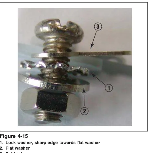
Both the order and orientation of mounting hardware need to be considered during assembly. Devices such as ‘‘star’’ or ‘‘tooth’’ washers may have one side with sharp edges intended to cut into the mating surface to keep the hardware from coming loose in operation. Figure 4-15 is an example of this kind of lock washer. Unless otherwise specified the sharp edges of the lock washer should be against the flat washer.
Acceptable – Class 1,2,3
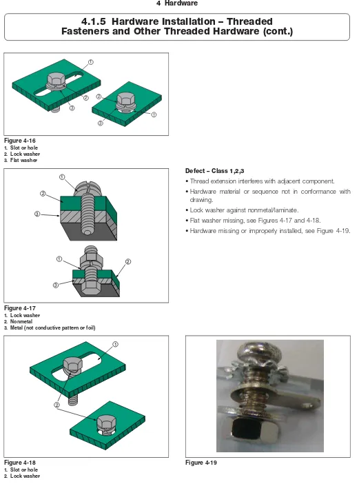
• Proper hardware sequence and orientation, see Figures 4-14 and 4-15.
• Slot or hole are covered with flat washer, see Figure 4-16.
Acceptable – Class 1 Defect – Class 2,3
• Less than one and one-half threads extend beyond the threaded hardware, (e.g., nut) unless thread extension would interfere with other component.
• Thread extension more than 3 mm [0.1 in] plus one and one-half threads for bolts or screws up to 25 mm [1 in]. • Thread extension more than 6.3 mm [0.25 in] plus one and
one-half threads for bolts or screws over 25 mm [1 in]. • Bolts or screws without locking mechanisms extend less
[image:31.612.66.310.200.427.2]than one and one-half threads beyond the threaded hard-ware. 1 2 2 3 4 3 4 1 Figure 4-14
1. Lock washer, sharp edge showing towards flat washer 2. Flat washer
3. Nonconductive material (laminate, etc.) 4. Metal (not conductive pattern or foil)
Figure 4-15
1. Lock washer, sharp edge towards flat washer 2. Flat washer
3. Solder lug
4 Hardware
[image:31.612.67.308.455.704.2]Defect – Class 1,2,3
• Thread extension interferes with adjacent component. • Hardware material or sequence not in conformance with
drawing.
• Lock washer against nonmetal/laminate. • Flat washer missing, see Figures 4-17 and 4-18.
• Hardware missing or improperly installed, see Figure 4-19.
1
2
3
2
3
1
Figure 4-16 1. Slot or hole 2. Lock washer 3. Flat washer
2
3
1
2 1
3
Figure 4-17 1. Lock washer 2. Nonmetal
3. Metal (not conductive pattern or foil)
1
[image:32.612.37.558.35.737.2]2
Figure 4-18 1. Slot or hole
Figure 4-19
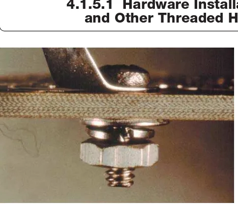
In addition to threaded fasteners used for installation of an item onto an assembly, there are other types of threaded items that may be used on individual parts within an assembly. These may require tightening to a specified torque value, or standard indus-try practice, to preclude loosening or part damage. Such items include, but are not limited to, connector coupling nuts, connec-tor strain relief clamps/potting/molding boots, etc., fuse holder mounting nuts, and any other similar threaded items.
Where torque requirements are not specified, follow standard industry practices. However, some of these threaded items may be made of plastic or other material that can be damaged if excessive torque is applied during assembly; and for these items, it may be necessary to tighten the item to a specified torque value.
Acceptable – Class 1,2,3
• Fasteners are tight and split-ring lock washers, when used, are fully compressed.
• Fastener torque value, if specified, is within limits.
• No evidence of damage resulting from over-tightening of the threaded item.
Figure 4-20
4 Hardware
Defect – Class 1,2,3
• Threaded items are not tight and split ring lock washer, if used, is not compressed, see Figure 4-21.
• Fastener torque value, if specified, is not within limits. • Hardware is loose, see Figure 4-22.
[image:34.612.44.286.62.270.2]• Evidence of damage resulting from over-tightening of the threaded item.
Figure 4-21
Figure 4-22
When the use of terminal lugs is not required, wires are wrapped around screw type terminals in a manner that precludes loos-ening when the screw is tightened, and the ends of the wire are kept short to preclude shorting to ground or other current carry-ing conductors.
If a washer is used, the wire/lead is mounted under the washer.
Unless otherwise noted, all requirements apply to both stranded and solid wires. Special hardware staking/securing criteria may be required.
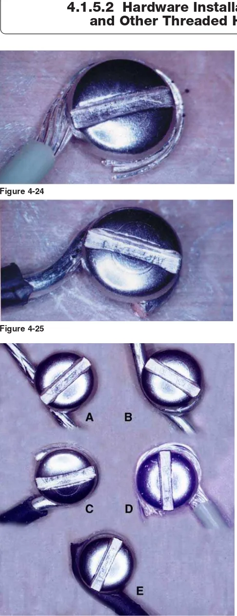
Target – Class 1,2,3
• Original lay of the strands is not disturbed (stranded wire). • Wire wrapped a minimum of 270° around the screw body. • Wire end secured under screw head.
• Wire wrapped in the correct direction. • All strands are under screw head.
Figure 4-23
4 Hardware
Acceptable – Class 1,2,3
• Less than one-third of the wire diameter protrudes from under the screw head.
• Wire extending outside the screw head does not violate minimum electrical clearance.
• Mechanical attachment of the wire is in contact between the screw head and the contact surface for a minimum of 180° around the screw head.
• No insulation in the contact area. • Wire does not overlap itself.
Defect – Class 1,2,3
• More than one-third of the wire diameter protrudes from under the screw head.
• Wire not wrapped around screw body, see Figure 4-26-A. • Wire is wrapped more than 360°, see Figure 4-26-B. • Solid wire wrapped in wrong direction, see Figure 4-26-C. • Stranded wire wrapped in wrong direction (tightening the
screw unwinds the twisted wire), see Figure 4-26-D. • Insulation in the contact area, see Figure 4-26-E. • Stranded wire is tinned (not shown).
[image:36.612.43.286.59.689.2]• Missing solder or adhesive as required per customer requirements (not shown).
Figure 4-24
Figure 4-25
Figure 4-26
This section covers the height relationship of the face of the jackpost to the associated connector face. This is critical to obtain maximum connector pin contact.
Hardware stack-up for mounted connectors may be varied in order to locate the face of the jackpost flush to 0.75 mm [0.030 in] below the face of the connector.
Acceptable – Class 1,2,3
• Jackpost face is flush to 0.75 mm [0.030 in] below the face of the connector.
• Height is obtained by adding or removing washers (supplied with jackpost).
Defect – Class 1,2,3
• Jackpost face extends above the connector face, see Figure 4-28.
• Face of jackpost is greater than 0.75 mm [0.030 in] below the connector face, see Figure 4-29.
Figure 4-27
Figure 4-28
Figure 4-29
4 Hardware
This section covers two types of pin installations; edge connector pins and connector pins. Installation of these devices is usually done with automated equipment. Visual inspection of this mechanical operation includes: correct pins, damaged pins, bent and broken pins, damaged spring contacts and damage to the substrate or conductive pattern. For connector mounting criteria see 7.1.8. For connector damage criteria see 9.5.
Acceptable – Class 1,2,3
• Contact is contained within the insulator, see Figure 4-30-A. • Gap is within specified tolerance, see Figure 4-30-B.
Note: To provide allowance for an extraction tool, the gap between the contact shoulder and the land needs to be adequate for each manufacturer’s repair tooling.
Defect – Class 1,2,3
• Contact is above insulator, see Figure 4-30-C.
• Gap between contact shoulder and land is greater than specified, see Figure 4-30-B.
B C
A
Figure 4-30
4.3 Connector Pins
Target – Class 1,2,3
• Pins are straight, not twisted and properly seated. • Pin height is within tolerance.
Acceptable – Class 1,2,3
• Pins are bent off center by 50% pin thickness or less.
Note:Nominal height tolerance is per pin connector or master drawing specification. The connector pins and mating con-nector must have a good electrical contact.
Figure 4-31
1. No discernible damage 2. Land
3. No discernible twist
Figure 4-32 1. Pin height tolerance 2. Less than 50% pin thickness
4 Hardware
Defect – Class 1,2,3
• Pin is bent out of alignment – bent off center greater than 50% pin thickness, see Figure 4-33.
• Pin visibly twisted, see Figure 4-34.
• Pin height is out of tolerance as to specification, see Figure 4-35.
Figure 4-33
Figure 4-34
Figure 4-35
Acceptable – Class 1,2,3
• No lifted or fractured annular rings with press fit pins.
Acceptable – Class 1,2
• Protrusion side land lifted less than or equal to 75% of the width (W) of the annular ring, Figure 4-36.
Acceptable – Class 2
• No visual evidence of lifted land on insertion side.
Acceptable – Class 3
• No lifted or fractured annular rings.
Defect – Class 1,2
• Any protrusion side functional annular ring lifted more than 75% of the width (W).
Defect – Class 2
• Any evidence of lifted lands on the insertion side.
Defect – Class 3
• Any lifted or fractured annular rings with press fit pins.
Note:For additional information see 10.3.2.
1 2 3 4 W Figure 4-36
1. Land lifted 75% ring or less 2. Land with conductor 3. Land not fractured
4. Land lifted, fractured but firmly attached land without conductor (nonfunctional) W 1 2 3 Figure 4-37 1. Land fractured
2. Functional land lifted greater than 75% of land width 3. Land lifted
4 Hardware
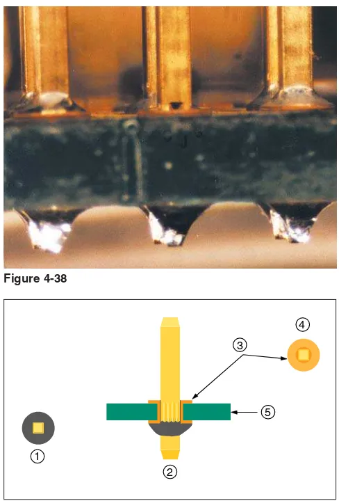
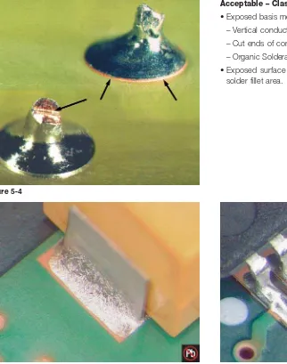
The term ‘‘press fit pins’’ is generic in nature and many types of pressure inserted pins, e.g., connector, staked, etc., are not intended to be soldered. If soldering is required the following criteria is applicable.
Target – Class 1,2,3
• A 360° solder fillet is evident on the protrusion side of the assembly.
[image:42.612.40.284.184.544.2]Note:Solder fillet or fill on insertion side is not required.
Figure 4-38
1
2
3
4
5
Figure 4-39 1. Bottom view 2. Side view 3. Land 4. Top view 5. PCB
Acceptable – Class 1,2
• Solder fillet or coverage protrusion side is present on two adjacent sides of the pin.
Acceptable – Class 3
• A 330° solder fillet is evident on the protrusion side of the assembly.
Acceptable – Class 1
• Solder wicking is permitted above 2.5 mm [0.1 in] on sides of pins provided there is no solder buildup that interferes with subsequent attachments to the pin.
Acceptable – Class 2,3
• Solder wicking on sides of pins is less than 2.5 mm [0.1 in], provided the solder does not interfere with subsequent attachments to the pin.
1
2
3
4
5
Figure 4-40 1. Bottom view 2. Side view 3. Land 4. Top view 5. PCB
2.5 mm [0.1 in]
Figure 4-41
4 Hardware
Defect – Class 1,2
• Solder fillet or coverage is evident on less than two adjacent sides of the pin on the protrusion side.
Defect – Class 3
• Less than 330° solder fillet on the protrusion side of the assembly.
Defect – Class 1,2,3
• Solder build up interferes with subsequent attachments to the pin.
Defect – Class 2,3
• Solder wicking exceeds 2.5 mm [0.1 in].
1
2
3
4
5
Figure 4-42 1. Bottom view 2. Side view 3. Land 4. Top view 5. PCB
Additional criteria can be found in IPC/WHMA-A-620.
Note:Do not subject wax impregnated lacing tape to cleaning solvents. Beeswax is unacceptable for Class 3.
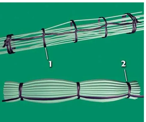
Target – Class 1,2,3
• Restraining devices are neat and tight, and spaced to keep the wires secured in a tight neat bundle.
• Restraining devices do not move.
• Restraining devices do not cause noticeable indentation or distortion of the wires of the assembly.
Figure 4-43
4 Hardware
4.4 Wire Bundle Securing
Acceptable – Class 1,2,3
• The end of the tie wrap/strap, see Figure 4-44:
– Protrudes a maximum of one tie wrap/strap thickness. – Is cut reasonably square to the face of the wrap. • The wires are secured in the wire bundle.
• Lacing or tie wraps/straps are placed on both sides of a wire breakout.
• Spot tie wraps/straps are neat and tight, see Figure 4-45. • The wires are secured in the wire bundle.
• Square knot, surgeons knot or other approved knot is used to secure the lacing.
• Restraining device does not have any longitudinal move-ment, but may rotate.
Figure 4-44
Figure 4-45
Acceptable – Class 1 Process Indicator – Class 2 Defect – Class 3
• The wire is under stress at the wrap, see Figure 4-46 left side.
• Spot ties or wraps/straps are under sleeving or markers. • Cut end of tie wrap/strap is greater than one wrap/strap
thickness, see Figure 4-46 right side.
Defect – Class 1,2,3
• Spot tie wrap/strap or knot is loose. • Spot tie wrap/strap cuts into the insulation. • Wire bundle is loose.
• Cable tied with an improper knot. This tie may eventually loosen.
• Bundle is distorted by the restraining devices.
• Insulation is compressed by more than 20% (see 6.2.1) or damaged by the restraining device.
• Restraining devices move longitudinally. Figure 4-46
Figure 4-47
Figure 4-48
4 Hardware
Lacing differs from cable ties because it is a continuous lace. Lacing has closer spacing than cable ties. Criteria for cable ties apply to lacing.
Note:Do not subject wax impregnated lacing tape to cleaning solvents. Beeswax is unacceptable for Class 3.
Acceptable – Class 1,2,3
• Lacing begins and ends with a locking knot.
• Lacing is tight and wires are kept secure in a neat bundle.
Defect – Class 1,2,3
[image:48.612.43.286.443.646.2]• Lacing is loose, leaving wires loose in the wire bundle (1). • Lacing is too tight, cutting into insulation (2).
Figure 4-49
Figure 4-50
Target – Class 1,2,3
• Restraining devices are not worn, frayed, nicked, or broken in any location.
• Restraining devices do not have sharp edges that may be a hazard to personnel or equipment.
Acceptable – Class 1,2
• Restraining devices exhibit minor fraying, nicks, or wear of less than 25% of the device thickness.
Defect – Class 1,2
• Damage or wear to restraining device greater than 25% of the device thickness, see Figure 4-52-A.
Defect – Class 3
• Damage or wear to restraining device, see Figure 4-52-A. • Cut end of lacing has not been heat seared.
• Heat searing touches knot. • Ends of lacing tape is frayed.
Defect – Class 1,2,3
• Sharp edges that are a hazard to personnel or equipment, see Figure 4-52-B.
• Broken lacing ends are not tied off using a square knot, sur-geons knot, or other approved knot, see Figure 4-52-C. Figure 4-51
Figure 4-52
4 Hardware
These criteria are applicable to single wires or wire bundles.
Wires in wire bundles are positioned to minimize crossover and maintain a uniform appearance.
Target – Class 1,2,3
• Wire lay is parallel to the axis of the bundle with no cross-over.
• Coaxial cable secured with tie wraps/straps.
Acceptable – Class 1,2,3
• Wires twist and crossover, but bundle is uniform in diameter.
Acceptable – Class 1 Process Indicator – Class 2 Defect – Class 3
• Wires twist and crossover underneath a tie wrap/strap.
Acceptable – Class 1 Defect – Class 2,3
• Bundle is not uniform in diameter. • Excessive crossover.
Defect – Class 1,2,3
• Any kinks that violate minimum bend radius. • Wire insulation is damaged, see 6.2.1. Figure 4-53
Figure 4-54
Figure 4-55
4.5 Routing – Wires and Wire Bundles
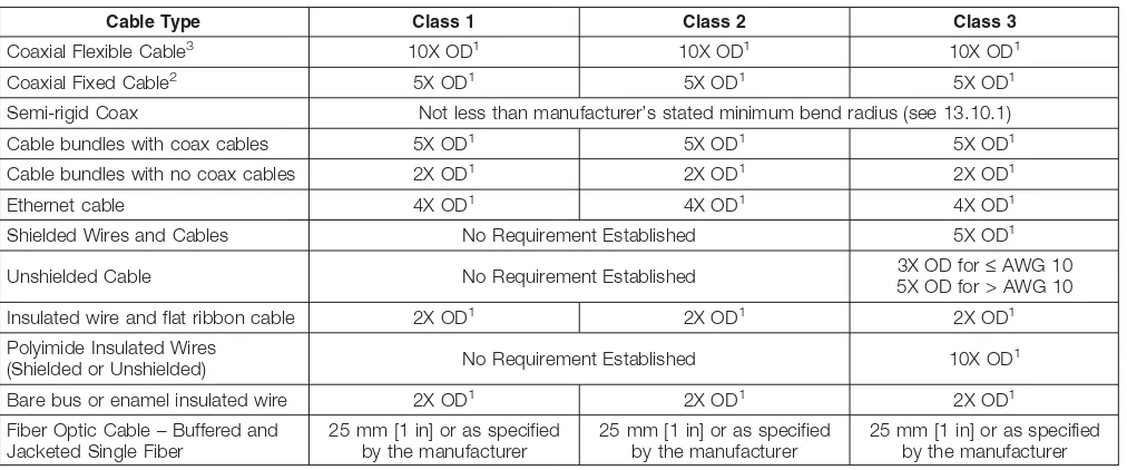
Bend radius is measured along the inside curve of the wire or wire bundles.
[image:51.612.67.573.171.382.2]The minimum bend radius of a harness assemblyshall not be less than whichever wire/cable in the assembly has the largest bend radius defined in Table 4-1.
Table 4-1 Minimum Bend Radius Requirements
Cable Type Class 1 Class 2 Class 3
Coaxial Flexible Cable3 10X OD1 10X OD1 10X OD1
Coaxial Fixed Cable2 5X OD1 5X OD1 5X OD1
Semi-rigid Coax Not less than manufacturer’s stated minimum bend radius (see 13.10.1) Cable bundles with coax cables 5X OD1 5X OD1 5X OD1
Cable bundles with no coax cables