RESEARCH STUDIES
ANTENNAS SERIES
Series Editor:
Professor J. R. James
The Royal Military College of Science
(Cranfield University), Shrivenham, Wiltshire,UK
10. Frequency Selective Surfaces: Analysis and Design
J. C. Vardaxoglou
11. Dielectric Resonator Antennas
Edited by
K. M. Luk
and
K. W. Leung
Dielectric Resonator Antennas
Edited By
K. M. Luk
and
K. W. Leung
Both of the City University of Hong Kong
RESEARCH STUDIES PRESS LTD.
www.research-studies-press.co.uk
and
Institute of PhysicsPUBLISHING, Suite 929, The Public Ledger Building, 150 South Independence Mall West, Philadelphia, PA 19106, USA
Copyright © 2003, by Research Studies Press Ltd.
Research Studies Press Ltd. is a partner imprint with the Institute of PhysicsPUBLISHING
All rights reserved.
No part of this book may be reproduced by any means, nor transmitted, nor translated into a machine language without the written permission of the publisher.
Marketing:
Institute of PhysicsPUBLISHING, Dirac House, Temple Back, Bristol, BS1 6BE, England
www.bookmarkphysics.iop.org
Distribution:
NORTH AMERICAAIDC, 50 Winter Sport Lane, PO Box 20, Williston, VT 05495-0020, USA
Tel: 1-800 632 0880 or outside USA 1-802 862 0095, Fax: 802 864 7626, E-mail: [email protected] UK AND THE REST OF WORLD
Marston Book Services Ltd, P.O. Box 269, Abingdon, Oxfordshire, OX14 4YN, England Tel: + 44 (0)1235 465500 Fax: + 44 (0)1235 465555 E-mail: [email protected]
Library of Congress Cataloguing-in-Publication Data
Dielectric resonator antennas / edited by K.M. Luk and K.W. Leung. p. cm.
Includes bibliographical references and index. ISBN 0-86380-263-X
1. Microwave antennas. 2. Dielectric resonators. I. Luk, K. M. (Kwai Man), 1958- II. Leung, K. W. (Kwok Wa), 1967 -
TK7871.67.M53 D54 2002 621.384' 135--dc21
2002069684
British Library Cataloguing in Publication Data
A catalogue record for this book is available from the British Library.
ISBN 0 86380 263 X
Printed in Great Britain by SRP Ltd., Exeter
Editorial Foreword
There is now a massive research literature on the Dielectric Resonator Antenna (DRA) giving ample evidence that the topic has reached an age of maturity. This new book is therefore very timely and fills a gap in the literature. In fact the absence of any such reference book to date, that collates research findings and significant achievements, is somewhat surprising in view of the growing interest in DRAs. Like microstrip antennas, DRAs offer many degrees of design freedom and exploit the properties of innovative materials that make possible the manufacture of stable low cost products. Again, like microstrip antennas, DRAs evolved from components in shielded microwave circuits where radiation is an unwanted by-product. Making use of the latter to create the DRA illustrates once again the ingenuity of antenna designers.
The reader will find the book coverage both wide and deep, with copious details of how to analyse and efficiently compute numerous DRA shapes and feeding arrangements. Engineering design data on extending the bandwidth and controlling the radiation pattern characteristics are focussed on throughout and specific chapters address DRA arrays and leaky-wave derivatives. When I visited the City University of Hong Kong in 1999 I was most impressed with Professor Luk’s research leadership and the dynamic environment in which he is working. Without doubt the enthusiasm of Kwai Man Luk and Kwok Wa Leung has energised both the writing of this book and their team of distinguished authors, many of whom, if not most, have made foremost contributions to this field of research.
The book will have widespread appeal to postgraduate researchers, antenna design engineers in general and particularly those engaged in the innovative design of mobile and wireless/Bluetooth systems. May I congratulate Professor Luk and Dr Leung and their co-authors on the production of this significant text, which will be a milestone in the advancement of the DRA concept and of great benefit to the international antenna community.
Preface
The field of wireless communications has been undergoing a revolutionary growth in the last decade. This is attributed to the invention of portable mobile phones some 15 years ago. The success of the second-generation (2G) cellular communication services motivates the development of wideband third-generation (3G) cellular phones and other wireless products and services, including wireless local area networks, home RF, Bluetooth, wireless local loops, local multi-point distributed networks (LMDS), to name a few. The crucial component of a wireless network or device is the antenna. Very soon, our cities will be flooded with antennas of different kinds and shapes. On the other hand, for safety and portability reasons, low power, multi-functional and multi-band wireless devices are highly preferable. All these stringent requirements demand the development of highly efficient, low-profile and small-size antennas that can be made imbedded into wireless products.
In the last 2 decades, two classes of novel antennas have been investigated and extensively reported on. They are the microstrip patch antenna and the dielectric resonator antenna. Both are highly suitable for the development of modern wireless communications.
The use of a dielectric resonator as a resonant antenna was proposed by Professor S. A. Long in the early nineteen eighties. Since the dielectric resonator antenna has negligible metallic loss, it is highly efficient when operated at millimetre wave frequencies. Conversely, a high-permittivity or partially-metallised dielectric resonator can be used as a small and low-profile antenna operated at lower microwave frequencies. Low loss dielectric materials are now easily available commercially at very low cost. This would attract more system engineers to choose dielectric resonator antennas when designing their wireless products.
principles, design guidelines and references for practicing engineers, research engineers, graduate students and professors specialising in the areas of antennas and RF systems.
The book was organised into a coherent order of proper perspectives, although we have over 10 contributors reviewing mainly their individual contributions. A historical perspective on the development of dielectric resonator antennas is provided in Chapter 1. Chapter 2 to 4 are more on rigorous analysis of dielectric resonator antennas of different geometries; in particular Chapter 2 on rectangular shapes, Chapter 3 on hemispherical shapes and Chapter 4 on cylindrical shapes. Although some wideband dielectric resonator antenna structures are introduced in these chapters, Chapter 5 reviews, in more detail, different bandwidth enhancement techniques, including the reduction of Q-factor by loading effect, the employment of matching networks, and the use of multiple resonators. In this era of wireless communications, low-profile and small-size antennas are highly preferable for mobile devices, such as cellular phones, notebook computers, personal digital assistant (PDA), etc. The design of low-profile dielectric resonator antennas is presented in Chapter 6, while the development of small compact circular sectored dielectric resonator antennas is described in Chapter 7. In these two chapters, techniques for the generation of circular polarisation are also included.
For applications requiring high-gain antennas, dielectric resonator antenna arrays may be a good choice. Chapter 8 introduces a new perpendicular feed structure suitable for antenna arrays with active circuits. Detailed study on linearly-polarised and circularly-polarised dielectric resonator arrays are reviewed in Chapter 9. A section of a non-radiative dielectric (NRD) guide can be considered as a rectangular dielectric resonator sandwiched between two parallel plates. With the introduction of an aperture-coupled microstripline feed, this simple structure, as described in Chapter 10, becomes an efficient antenna element with reasonably high gain. This novel antenna, which is leaky and resonant in nature, is designated as a NRD resonator antenna. Due to its low-loss characteristic, the antenna is highly attractive for wideband mobile communication systems operated at millimetre waves.
We would like to express our heartiest thanks to Professor J. R. James who has provided strong support and valuable suggestions to the preparation of this first book on dielectric resonator antennas. Special thanks also go to all chapter contributors. The encouragement from Professor Stuart A. Long is gratefully acknowledged.
Kwai Man Luk and Kwok Wa Leung
Contents
Abbreviations and Symbols xv
CHAPTER 1 Overview of the Dielectric Resonator Antenna
By K. W. Leung and S. A. Long
1.1 Introduction 1
1.2 Excitation methods applied to the DRA 4
1.3 Analyses of the DRA 4
1.3.1 Cylindrical DRA 4
1.3.1.1 Resonant frequencies 4
1.3.1.2 Equivalent magnetic surface currents 8
1.3.1.3 Far-field patterns 8
1.3.1.4 Results 10
1.3.1.4.1 Input impedance and resonant frequency 10
1.3.1.4.2 Radiation patterns 12
1.3.2 Hemispherical DRA 13
1.3.2.1 Single TE111-mode approximation 14
1.3.2.2 Single Tm101-mode approximation 18
1.3.2.3 Rigorous solution for axial probe feed 20
1.3.3 Rectangular DRA 23
1.4 Cross-polarisation of probe-fed DRA 23
1.5 Aperture-coupled DRA with a thick ground plane 26
1.6 Simple results for the slot-coupled hemispherical DRA 30
1.7 Low-profile and small DRAs 33
1.8 Broadband DRAs 34
1.9 Circularly polarised DRAs 34
1.10 DRA arrays 37
1.11 Air gap effect on the DRA 45
1.12 Conclusion 45
1.13 Appendix 46
References 47
CHAPTER 2 Rectangular Dielectric Resonator Antennas
By Aldo Petosa, Apisak Ittipiboon, Yahia Antar
2.1 Introduction 55
2.2 Dielectric waveguide model for rectangular dielectric guides 56
2.3.1 Field configuration 60
2.3.2 Resonant frequency 61
2.3.3 Q-factor 64
2.4 Radiation model 67
2.5 Finite ground plane effects 67
2.6 Coupling methods to DRAs 69
2.6.1 Review of coupling theory 70
2.6.2 Slot aperture 72
2.6.3 Coaxial probe 72
2.6.4 Microstrip line 73
2.6.5 Co-planar feeds 74
2.6.6 Dielectric image guide 76
2.7 Radiation efficiency of a rectangular DRA 77
2.8 Numerical methods for analysing DRAs 81
2.9 Summary 88
References 89
CHAPTER 3 Analysis of Multi-Layer Hemispherical DR Antennas
By Kin-Lu Wong
3.1 Introduction 93
3.2 A probe-fed DR antenna with an air gap 94
3.2.1 Green’s function formulation 94
3.2.2 Single-mode approximation 100
3.2.3 Numerical results and discussion 101
3.3 A probe-fed DR antenna with a dielectric coating 104
3.3.1 Green’s-function formulation 106
3.3.2 Numerical results and discussion 108
3.4 A slot-coupled DR antenna with a dielectric coating 112
3.4.1 Theoretical formulation 112
3.4.2 Numerical results and discussion 120
References 124
CHAPTER 4 Body of Revolution (BOR) - Analysis of Cylindrical
Dielectric Resonator Antennas By Ahmed A. Kishk
4.1 Introduction 127
4.2 Formulation of the problem 128
4.2.1 Wire probe excitation 128
4.2.2 Method of moments 131
4.2.3 Narrow slot excitation 136
4.2.4 The slot-coupled microstrip line feed 138
4.3 Resonant frequency and radiation Q-factor 141
4.5 Far fields 146
4.5.1 Ideal far field patterns 146
4.5.2 Far field radiation patterns due to dipole excitation 147
4.5.3 Far field radiation patterns due to narrow slot excitation 151
4.5.4 Verifications of the radiation patterns 154
4.5.5 DRA feed for parabolic reflector 155
4.6 Input impedance 159
4.6.1 Wire probe excitation 159
4.6.2 Slot excitation 164
Acknowledgement 168 References 169
Miscellaneous references 172
CHAPTER 5 Broadband Dielectric Resonator Antennas
By Aldo Petosa, Apisak Ittipiboon, Yahia Antar
5.1 Introduction 177
5.2 Bandwidth of rectangular and cylindrical DRAs 179
5.3 Bandwidth enhancement with single DRAs 181
5.3.1 Probe-fed rectangular DRA with air gap 182
5.3.2 Annular DRAs 184
5.3.3 Notched rectangular DRAs 187
5.4 Bandwidth enhancements using impedance matching 187
5.4.1 Flat matching strips 189
5.4.2 Loaded notched DRAs 190
5.4.3 Multi-segment DRAs 190
5.4.4 Stub matching 200
5.5 Bandwidth enhancement using multiple DRAs 200
5.5.1 Co-planar parasitic DRAs 203
5.5.2 Stacked DRAs 206
5.6 Summary 207
References 208
CHAPTER 6 Low-Profile Dielectric Resonator Antennas
By Karu Esselle
6.1 Introduction 213
6.2 Linearly polarised rectangular DR antennas 213
6.2.1 Aperture-coupled rectangular DR antennas 214
6.2.2 Co-planar waveguide-fed rectangular DR antennas 222
6.3 Circularly polarised rectangular DR antennas 224
6.4 Linearly polarised circular disk DR antennas 228
6.5 Circularly polarised dielectric disk antennas 230
6.6 Linearly polarised triangular DR antennas 234
6.8 Conclusions 240
References 241
CHAPTER 7 Compact Circular Sector and Annular Sector Dielectric
Resonator Antennas For Wireless Communication Handsets By R. D. Murch and T. K. K. Tam
7.1 Introduction 245
7.1.1 Challenges 246
7.1.2 Approaches 247
7.1.3 Section Summary 247
7.2 Dielectric resonator antennas 248
7.2.1 Features 248
7.2.2 Geometries 248
7.2.3 Resonant modes 249
7.2.4 Circular cylindrical DRAs 249
7.2.5 Excitation schemes 251
7.2.6 Dielectric resonator antenna modelling 256
7.3 Compact circular sector and annular sector DRAs 256
7.3.1 General geometry 257
7.3.2 An approximate cavity model 257
7.3.2.1 Conventional circular DRA 258
7.3.2.2 Circular sector DRA 258
7.3.2.3 Annular DRA 261
7.3.2.4 Annular sector DRA 263
7.3.3 Simulation results 264
7.3.4 Experimental results 264
7.3.5 Compact DRA designs 265
7.3.5.1 Minimum volume DRAs 266
7.3.5.2 Minimum profile DRAs 267
7.3.6 Proposed PCS antenna design 267
7.3.7 Summary 271
7.4 DRA designs for circular polarisation 272
7.4.1 Polarisation of waves 272
7.4.2 Existing DRA approaches 273
7.4.2.1 Theory 274
7.4.3 Design considerations 276
7.4.4 Simulation results 277
7.4.5 Experimental results 277
7.4.6 Summary 281
7.5 Dual frequency DRA 282
7.5.1 Theory 282
7.5.2 Simulations and experiments 285
7.5.3 Summary 286
7.6.1 Circular sector DRAs 288
7.6.2 Circularly polarised sector DRA 288
7.6.3 Dual frequency sector DRA 288
7.6.4 Further developments 289
References 290
CHAPTER 8 Feeding Methods for the Dielectric Resonator Antenna:
Conformal Strip and Aperture Coupling with a Perpendicular Feed
By K. W. Leung
8.1 Introduction 293
8.2 Conformal strip excitation 295
8.2.1 DRA Green’s function 295
8.2.2 Moment method solution for the strip current 297
8.2.3 Evaluation of Zpq 299
8.2.4 Radiation fields 300
8.2.5 Results 302
8.3 Aperture-coupled DRA with a perpendicular feed 306
8.3.1 Theory 306
8.3.2 The DRA admittances Ymna 312
8.3.3 Results 313
8.4 Conclusion 314
8.5 Appendix A 316
8.6 Appendix B 318
References 319
CHAPTER 9 Dielectric Resonator Antenna Arrays
By Z. Wu
9.1 Introduction 321
9.2 Parameters of DRA arrays 321
9.2.1 DRA elements and feed arrangement 321
9.2.2 Array factors of linear and planar arrays 323
9.2.3 Mutual coupling between DRAs 328
9.3 Linearly polarised linear DRA arrays 331
9.3.1 Slot-coupled linear DRA arrays with microstrip corporate feed 331 9.3.2 Probe-coupled linear DRA arrays with microstrip corporate feed 336
9.3.3 Microstrip-coupled linear DRA arrays 339
9.4 Linearly polarised planar DRA arrays 341
9.4.1 Slot-coupled planar DRA arrays with microstrip corporate feed 341 9.4.2 Probe-coupled planar DRA arrays with microstrip corporate feed 344
9.4.3 Microstrip-coupled planar DRA arrays 346
9.5 Circularly polarised DRA arrays 347
9.7 Discussion and conclusions 352
References 352
CHAPTER 10 Leaky-Wave Dielectric Resonator Antennas Based on NRD
Guides
By K. M. Luk and M. T. Lee
10.1 Introduction 355
10.1.1 Antennas based on NRD guides 355
10.1.1.1 Feeding methods 356
10.1.1.2 Generation of leaky waves 357
10.1.2 Leaky-wave antennas using asymmetric NRD guide 359
10.1.2.1 Principle of operation 360
10.1.2.2 Applications 360
10.2 Leaky-wave dielectric resonator antennas based on 360
symmetric image NRD guides
10.2.1 Rectangular leaky-wave DRA 361
10.2.1.1 Antenna characteristics 361
10.2.1.2 Effect of height of parallel plates 363
10.2.1.3 Effect of using unequal parallel plates 365
10.2.1.4 Discussion 367
10.2.2 Inverted T-shaped leaky-wave DRA 368
10.2.2.1 Experimental results 369
10.2.2.2 Discussion 372
10.2.3 Summary 372
10.3 Leaky-wave dielectric resonator antennas based on 373
asymmetric NRD guides
10.3.1 Using asymmetric inverted T-shaped dielectric slab 373
10.3.1.1 Experimental results 373
10.3.1.2 Summary and discussion 376
10.3.2 Using staircase-shaped dielectric slab 376
10.3.2.1 Experimental results 378
10.3.2.2 Discussion 379
10.4 Conclusion 380
Acknowledgement 382 References 382
Abbreviations and Symbols
AF array factor
AR axial ratio
BOR body of revolution
BW bandwidth
CP circular polarisation
CPW co-planar waveguide
Copol co-polarisation dB decibel
D diffraction coefficient
DBOR dielectric body of revolution
DOA direction of arrival
DR dielectric resonator
DRA dielectric resonator antenna
E electric field
f frequency
F normalised frequency
FDTD finite-difference time-domain
FEM finite-element method
GO geometric optics
GPS global positioning system
GSM group special mobile
GTD geometric theory of diffraction
H magnetic field
HE hybrid electric
HEM hybrid electromagnetic
HFSS high frequency structure simulator
)
(
ˆ
(2)x
H
n Schelkunoff-type spherical Hankel function of the second kindof order n
)
(
x
J
n cylindrical Bessel function of order n)
(
ˆ
x
J
n Schelkunoff-type spherical Bessel function of the first kind of order nk wave number
LAN local area network
LP linear polarisation
LHCP left-hand circular polarisation
LNA low-noise amplifier
LSM longitudinal section magnetic
ME modal expansion
MoM method of moments
MSDRA multi-segment dielectric resonator antenna
NRD non-radiative dielectric
)
(
x
P
n Lengendre polynominal of order n)
(
x
P
mn associated Lengendre function of the first kind of order m and
degree n
PCS personal communication system
PD phase detector
PMWM perfect magnetic wall model
PWS piecewise sinusoidal
Q-factor quality factor
RF radio frequency
RHCP right-hand circular polarisation
SDM spectral domain method
SWR standing-wave ratio
TE transverse electric
TEM transverse electromagnetic
TLM transmission line method
TM transverse magnetic
VSWR voltage standing wave ratio
XDRA cross dielectric resonator antenna
CHAPTER 1
Overview of the Dielectric
Resonator Antenna
Kowk Wa Leung* and Stuart A. Long
+* Department of Electronic Engineering
City University of Hong Kong
Kowloon, Hong Kong SAR
+ Department of Electrical and Computer Engineering
University of Houston
TX 77204-4005, USA
1.1 INTRODUCTION
For many years, the dielectric resonator (DR) has primarily been used in microwave circuits, such as oscillators and filters [1], where the DR is normally made of high-permittivity material, with dielectric constant εr > 20. The unloaded
Fig. 1.1 DRAs of various shapes. The photo shows cylindrical, rectangular, hemispherical, low-profile circular-disk, low-profile triangular, and spherical-cap DRAs.
As compared to the microstrip antenna, the DRA has a much wider impedance bandwidth (~ 10 % for dielectric constant εr ~ 10). This is because the microstrip
antenna radiates only through two narrow radiation slots, whereas the DRA radiates through the whole DRA surface except the grounded part. Avoidance of surface waves is another attractive advantage of the DRA over the microstrip antenna. Nevertheless, many characteristics of the DRA and microstrip antenna are common because both of them behave like resonant cavities. For example, since the dielectric wavelength is smaller than the free-space wavelength by a factor of 1/ εr , both of them can be made smaller in size by increasing εr. Moreover,
Company Material Dielectric Constant
Countis Laboratories CD-Series (solid state solutions of magnesium, calcium, silicon, and titanium oxides)
6.3 − 140.0
Emerson & Cuming (Materials not specified)
Eccostock 3 − 30
Magnesium Manganese Aluminum Iron Ferrite
9.2 (+/- 0.46)
Magnesium Titanate 16.0 (± 0.8)
Lithium Ferrite 20.0 (± 1)
Zirconium Tin Titanate 37.0 (± 1)
Hiltek Microwave Ltd.
Titania Ceramic 80 − 100
Zr, Sn titanate 37
Mg, Ca titanate 20
Ba, Nd titanate 88
Ba, Zn titanate 30
Morgan Electro Ceramics
Steatile 6
U series 36.6 – 38.9 (± 0.5)
M series 37.7 – 39.2 (± 1)
V series 33.5 – 35.1 (± 0.5)
R series 29.7 – 31.5 (± 0.8)
B series 27.9 ± 0.5
E series 24.2 – 24.9 (± 0.4)
F series 23.8 – 24.2 (± 0.5)
Murata
(Materials not specified)
Dielectric substrate 38 – 92 (± 1)
Pacific Ceramics, Inc. (Materials not specified)
PD-Series 6.5 − 270
(Zr, Sn, Ti) O4 37.3 – 37.7
Ba, Zn, Ta, O 29.5 – 32
Temex Components & Temex Telecom
Ba, Sm, Ti 78 ± 0.5
Zirconium titanate based 44.7 – 46.2
Ba, Zn, Ta-oxide 29.0 – 30.7
Barium titanate 35.0 – 36.5
Trans-Tech
Ba, Zn, Ta-oxide (perovskite) 29.5 – 31.0 Table 1.1 Some DR suppliers, along with the materials and dielectric constants of
This book has ten chapters on various topics concerning the DRA. For quick reference, Table 1.2 lists some sections of those chapters that address bandwidth, efficiency, and radiation patterns in a more detailed fashion.
Section
Bandwidth 2.3.3, 3.2.3, 3.3.2, 5.2-5.5, 6.2.1, 7.3.4, 10.2.2.1, 10.3.1.1, 10.3.2.1
Efficiency 2.7, 9.3, 9.4 Radiation
Pattern
2.4, 2.5, 3.2.3, 4.5, 5.3 – 5.5, 6.2.1, 6.3-6.7, 7.4.4, 7.4.5, 9.2.2, 9.3-9.5, 10.2.1.2, 10.3.2.1
Table 1.2 Quick references for bandwidth, efficiency, and radiation pattern.
1.2 EXCITATION METHODS APPLIED TO THE DRA
A number of excitation methods have been developed. Examples are the coaxial probe [5-7, 13-15], aperture-coupling with a microstrip feedline [8, 9, 15-23], aperture-coupling with a coaxial feedline [24, 25], direct microstrip feedline [26, 27], co-planar feed [28], soldered-through probe [11], slotline [29], stripline [30], conformal strip [31-33], and dielectric image guide [34]. A photo of the coaxial probe excitation scheme is shown in Fig. 1.2, and that of the aperture-coupling excitation scheme is given in Fig. 1.3. Some of the feeding methods are addressed in Chapter 2, whereas the rigorous analyses of the aperture coupling with a perpendicular feed [22] and conformal strip feed [31] are presented in Chapter 8.
1.3 ANALYSES OF THE DRA
1.3.1 Cylindrical DRA
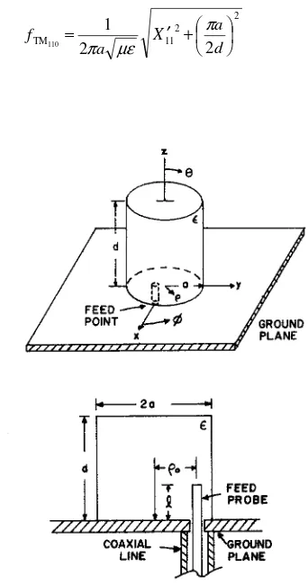
A simple analysis for the cylindrical DRA was carried out in [5] using the magnetic wall model. Fig. 1.4 shows the DRA configuration, along with standard cylindrical coordinates.
1.3.1.1 Resonant frequencies
(a)
(b)
(a)
(b)
where Jn is the Bessel function of the first kind, with Jn
( )
Xnp =0 ,Jn′( )
Xnp′ =0 ,n = 1,2, 3, ⋅⋅⋅, p = 1, 2, 3, ⋅⋅⋅, m = 0, 1, 2, 3, ⋅⋅⋅
From the separation equation ρ ω µε
2 2 2 2+k =k =
k z , the resonant frequency of
the npm mode can be found as follows:
In practical applications, we are interested in the fundamental (dominant) mode, which has the lowest resonant frequency. It is found that the fundamental mode is the TM110 mode, with the resonant frequency given by
2
1.3.1.2 Equivalent magnetic surface currents
The TM110-mode fields inside the cylindrical DRA are used for thederivation of
the far-field expressions. To begin, the wave function of the fundamental TM110
mode is found: the various E-fields can be easily found:
z
Use is made of the equivalence principle to find the equivalent magnetic currents on the DRA surfaces. The equivalent currents will be treated as the radiating sources for the radiation fields. In the following expressions, the primed and unprimed coordinates are used to indicate the source and field, respectively. From
n E
Mr = r׈, where
n
ˆ
is a unit normal pointing out of the DRA surface, the following equivalent currents are obtained:(i) for theside wall
Usually, radiation fields are expressed in spherical coordinates (r, θ, φ). Therefore the source currents are transformed:
The transformed currents are used in calculations of the electric vector potentials: electric potentials are given by
(
)
(
)
In the far-field region, the electric fields Eθ, Eφ are proportional to the vector
1.3.1.4 Results
1.3.1.4.1 Input impedance and resonant frequency
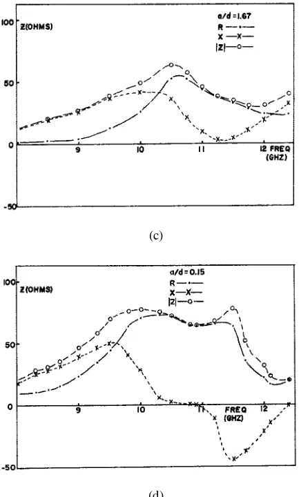
Since the input impedance cannot be calculated using the magnetic wall model, the input impedance studied in [5] was solely experimental. Four cylindrical DRAs of dielectric constant εr = 8.9 were fabricated with radius-to-height ratios a/d = 0.3,
0.5, 1.67, and 0.15. Each DRA was fed near its edge by a coaxial probe that extended l = 0.38 cm into the DRA. The results are reproduced in Fig. 1.5. Note that for a/d = 0.15 (Fig. 1.5 d) the first two modes, TM110 and TM111 modes, are
very close to each other in frequency, corresponding to the predicted values of 9.90 and 10.52 GHz, respectively.
(a)
(c)
(d)
Fig. 1.5 Measured impedance versus frequency for various a/d ratios: εr = 8.9. (a)
a/d = 0.3 (b) a/d = 0.5 (c) a/d = 1.67 (d) a/d = 0.15. (From [5], © 1983 IEEE)
Table 1.3 compares the calculated and measured TM110-mode resonant
was taken at the point where the resistance is a maximum, and good agreement between theory and experiment is obtained.
Sample no. a (cm) d (cm) a/d Calculated fr ,GHz Measured fr ,GHz
1 0.3 1.0 0.3 10.13 ~10.1
2 0.3 0.6 0.5 10.67 ~10.5
3 0.5 0.3 1.67 10.24 ~10.5
4 0.3 2.0 0.15 9.90 ~9.9
Table 1.3 Comparison between calculated and measured resonant frequencies.
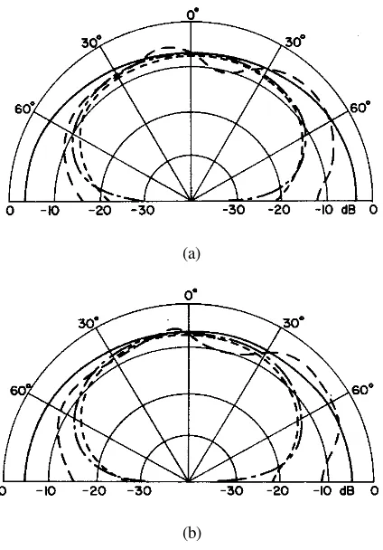
1.3.1.4.2 Radiation patterns
Fig. 1.6 shows the calculated and measured field patterns for the four cylindrical DRAs. Reasonable agreement is observed for the first three DRAs, with the only differences being some scalloping and a roll-off near θ = 90o for the measured
values of Eθ due to the finite ground plane. For the last case of a/d = 0.15, a dip near θ = 0o is observed in both the measured and calculated results.
(a)
(c)
(d)
Fig. 1.6 Measured and calculated fields of various a/d ratios: (a) a/d = 0.3 (b) a/d = 0.5 (c) a/d = 1.67 (d) a/d = 0.15. (From [5], © 1983 IEEE)
Eθ: Theory Eθ: Experiment Eφ: Theory Eφ: Experiment
A rigorous analysis of the cylindrical DRA was carried out by Junker et al. [13] using the body of revolution (BOR) method. Details of the analysis can be found in Chapter 4. Alternatively, Shum and Luk used the finite-difference time-domain (FDTD) method [14, 15] to analyze the cylindrical DRA.
1.3.2 Hemispherical DRA
cylindrical shapes in that the interface between the dielectric and air is simpler; and thus, a closed form expression can be obtained for the Green’s function.
Fig. 1.7 Configuration of a probe-fed hemispherical DRA. (From [36], © 1993 IEEE)
The theory is summarised here. The field and source points are denoted by ) directed current will excite both TE and TM to r modes, the magnetic potential, Fr,
as well as the electric potential, Ar, are required to represent all possible fields.
Conversely, an r-directed current can excite only TM to r modes, and therefore only the electric potential is required in this case. Each potential function is represented by an infinite series of modal functions. The modal coefficients are then obtained by matching the boundary conditions at the source point and on the DRA surface. The detailed analysis can be found in [36].
1.3.2.1 Single TE111-mode approximation
At frequencies around the TE111-mode resonance, we may take the single-mode
approximation [35, 37]. As a result, the z-component of the E-field Green’s function inside the DRA is given by (r < a):
Hemispherical DRA Coaxial probe
[
ˆ ( ) ˆ '( ) ˆ '( ) ˆ ( )]
the first-order spherical Bessel function of the first kind and spherical Hankel function of the second kind, respectively. A prime denotes a derivative with respect to the whole argument, except that r′ denotes the source point. From the Green’s function
111
TE
G , the z-directed electric field Ez due to the probe current Jz
can be evaluated as follows:
∫∫
′ ′ ′is the assumed surface current flowing on the imaged probe surface S0. The input
impedance is then determined using the variational formula:
dS
The input impedance obtained by (1.35) is correct to second order for an assumed current distribution Jz which is correct to first order [38]. The input impedance
given by (1.35) is the input impedance of the imaged configuration. To obtain the input impedance of the original configuration, the impedance, Zin , should be divided by two.
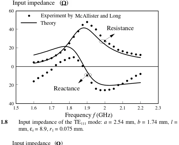
The calculated TE111-mode input impedance, using the above theory, is
conveniently compared with the previous measurement made by McAllister and Long [7]. The DRA used in [7] had a radius of 2.54 cm, with εr = 8.9, and a probe
measured value of 1.90 GHz. Measured and predicted bandwidths also match reasonably well at 10.3 and 13.1 %, respectively.
Fig. 1.9 shows the variation of the input impedance with frequency for different probe lengths [37]. It is observed that while the input impedance increases significantly with probe length, the resonant frequency shifts only slightly. It is in contrast to the bare monopole case, in which the resonant frequency will vary considerably with probe length.
Fig. 1.8 Input impedance of the TE111 mode: a = 2.54 mm, b = 1.74 mm, l = 1.52
mm, εr = 8.9, r1 = 0.075 mm.
Fig. 1.9 Input impedance of the TE111 mode for different probe lengths: a = 2.54
mm, b = 1.74 mm, εr = 8.9, r1 = 0.075 mm.
1.5 1.6 1.7 1.8 1.9 2 2.1 2.2 2.3
40 20 0 20 40 60
Resistance
Reactance Input impedance ( )ΩΩΩΩ
Frequency f (GHz)
Experiment by Theory
McAllister and Long
1.5 1.6 1.7 1.8 1.9 2 2.1 2.2 2.3
-60 -40 -20 0 20 40 60 80 00
Input impedance ( )ΩΩΩΩ
Frequency f (GHz) l=1.2cm
l=1.6cm l=1.8cm
Resistance
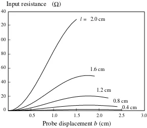
The variation of input resistance at resonance with feed position for different probe lengths is shown in Fig. 1.10. The input resistance increases as the probe is displaced away from the DRA center, until a maximum point is reached. It then decreases slightly as the displacement increases further. Note that the input resistance is small when b is small. This is caused by the fact that the TE111 mode
cannot be excited properly when the feed position is near the center, since in this case the probe current is dominated by the r-directed component, which excites TM modes only. From the figure, it is seen that the longer the probe length is, the higher the input resistance.
Fig. 1.10 Input resistance calculated at TE111-mode resonance versus probe
displacement b: a = 2.54 mm, f = 1.88 GHz, εr = 8.9, r1 = 0.075 mm. (From
[35], reprinted with permission from IEE)
Fig. 1.11 shows the resonant input resistance of the TE111 mode as a function
of εr [37]. As can be observed, the input resistance increases with εr. Again, the
longer the probe length is, the higher the input resistance.
Input resistance ( )
Ω
0 20 40 60 80 00 20 40
0.5
Probe displacement
b
(cm)
1.0 1.5 2.0 2.5 3.0
l = 2.0 cm
1.6 cm
1.2 cm
Fig. 1.11 Input resistance of the TE111 mode at resonance versus dielectric constant
εr: a = 2.54 mm, b = 1.74 GHz, f =
111
TE
f , r1 = 0.075 mm.
1.3.2.2 Single Tm101-mode approximation
A similar study was carried out for the TM101 mode of the hemispherical DRA [37,
39]. The TM101-mode Green’s function is given by
[
]
the input impedance, (1.35) is applied again here, except only that the Green’s function
101
TM
G is in place of
111
TE
G . Moreover, the same current density given by (1.33) is assumed along the imaged probe.
An experiment was carried out in [39] to verify the theory. In the experiment, a hemispherical DR with εr = 9.8 and radius 11.5 mm was used. The DR was
mounted on a 60×60 cm copper ground plane and fed by a coaxial launcher with a probe diameter of 1.25 mm, penetrating 4.5 mm into the dielectric. The input impedance as a function of frequency is shown in Fig. 1.12 [37]. From the theory, the resonant frequency is 5.85 GHz, which is very close to the measured value of 5.95 GHz. In view of the predicted resonant frequency of 5.70 GHz obtained by solving the characteristic equation ∆TM = 0 (Eq. 1.38), the results are quite
consistent. Reasonably good agreement is observed for the bandwidth (20.4 % measured versus 23.5 % calculated). The TM101-mode input impedance was
studied for different probe lengths. The results are similar to those of the TE111
mode and are therefore omitted here.
Fig. 1.12 Input impedance of the TM101 mode versus frequency: a = 11.5 mm, b =
0.0 mm, l = 4.5 mm, εr = 9.8, r1 = 0.075 mm.
The effect of εr on the TM101-mode input impedance is shown in Fig. 1.13.
While it has been found that the TE111-mode input resistance increases linearly
with εr, the TM101-mode input resistance is seen to increase exponentially with εr.
It is because Hφ , which is tangential to the DRA surface, is the only magnetic field
for the TM101 mode. Thus, the fields of the TM101 mode are of a confined mode
[40], i.e., the DRA surface can be treated as a real magnetic wall as εr→∞. Since
the resonance is of a parallel type, the magnetic wall effect causes the input resistance to increase, and the radiation decreases, rapidly with εr.
4 4.5 5 5.5 6 6.5 7 7.5 8
20 10 0 10 20 30 40
Input impedance ( )Ω
Frequency f (GHz)
Experiment
Theory Resistance
Fig. 1.13 Input resistance of the TM101 mode at resonance versus dielectric constant
εr for different probe lengths: a = 11.5 mm, b = 0.0 GHz, l = 4.5 mm, f =
101
TM
f , r1 = 0.63 mm. (From [39], © 1993 John Wiley & Sons, Inc.)
1.3.2.3 Rigorous solution for axial probe feed
When the DRA is fed axially, only TM modes can be excited. In this special case, a rigorous and yet simple general solution can be obtained [41]. Using the result of [36], the Green’s function for a thin dipole (or imaged monopole) embedded inside a spherical DR (or grounded hemispherical DR) can be given by
)
is the TM-mode reflection coefficient at the DRA boundary and
2
of TM n
α for n = 1. The method of moments (MoM) with Galerkin’s procedure is used to solve forthe probe current. To begin, the current is expanded as
∑
where fq(z) is a piecewise sinusoidal (PWS) function given by
and the PWS mode half-length, respectively. The unknown expansion coefficients
Iq’s are solved via the matrix equation
)]
The result for efficient calculations of the impedance integral ZPpq can be found in [42]. Here we concentrate on obtaining a computationally efficient expression for the integral ZHpq. To begin, we write ZHpq as
implementation of (1.45) is very easy. The only care that has to be exercised is that
uij may be zero for some i,j, for which Jˆn(kuij)= 0. Therefore, uij should be
checked in the program, as the (backward) recurrence formula for Jˆn(x) cannot be used when x = 0. After the Iq’s are found, the input impedance can be obtained
by simply using Zin =
∑
=N
n1Infn(0)
β , where β = 1 for the equivalent dipole
configuration and β = 1/2 for the original (monopole) configuration.
When only the first term (n = 1) is taken, an even simpler result can be
Fig. 1.14 compares the input impedances calculated from the theory for n = 1 with that of the rigorous solution [36] for different probe lengths. The comparison for different dielectric constants is given in Fig. 1.15. Three expansion modes (N = 3) were used for the current. With reference to the figures, the present theory agrees almost exactly with the rigorous one. The case for different DRA radii was also studied; and, again, excellent agreement between the simplified and rigorous theories was observed.
Fig. 1.14 Input impedance versus frequency for different probe lengths: a = 12.5 mm, εr = 9.5, r1 = 0.63 mm. (From [43], reprinted with permission from
Lines : Rigorous Theory Dots : Simple formula
Fig. 1.15 Input impedance versus frequency for different dielectric constants: a = 12.5 mm, l = 5.0 mm, r1 = 0.63 mm. (From [43], reprinted with permission
from IEE)
1.3.3 Rectangular DRA
The rectangular DRA is even more difficult to analyze than the cylindrical one because of the increase in edge-shaped boundaries. Usually the dielectric waveguide model is used to analyze the problem [44-47]. In this approach, the top surface and two sidewalls of the DRA are assumed to beperfect magnetic walls;
whereas the two other sidewalls are imperfect magnetic walls. Since normally the DRA resides on a conducting ground plane, an electric wall is assumed for the bottom surface. With these assumptions, the fields of the DR are expanded in TE and TM modes using the modal expansion (ME) method. The fields inside and outside the DRA are expressed in terms of sinusoidal and exponentially decaying functions, respectively. The wave propagation numbers and attenuation constants are then found by matching the boundary conditions. Details can be found in Chapter 2.
A more accurate, but time-consuming, approach is to use the FDTD method, which was adopted by Shum and Luk [48] in analyzing the aperture-coupled rectangular DRA.
1.4 CROSS-POLARISATION OF PROBE-FED DRA
For radiation patterns of the DRA residing on an infinite ground plane, theoretical studies were focused only on the co-polarised (copol) fields [49]. However, the cross polarisation is also an important consideration in antenna design [50]. Furthermore, for probe-fed excitation, the impedance matching is usually achieved by varying the probe length and/or probe displacement. Apart from these
2.5 3 3.5 4 4.5 5 5.5 6 6.5
-60 -40 -20 0 20 40 60 80 100
Frequency (GHz) Input impedance (Ω)
Lines : Rigorous Theory Dots : Simple formula
εr= 20.0
εr= 15.0
parameters, the dielectric constant εr can also be used in the DRA design. For
example, it can be used to change the resonant (operation) frequency, since as the dielectric constant increases, the resulting resonant frequency is reduced. The effects of these design parameters on the cross-polarisation level are of interest. Leung et al. [51] studied the cross-polarisation characteristics of a probe-fed hemispherical DRA, which is excited in the fundamental TE111 mode. It should be
mentioned that as DRAs of different shapes show very similar behavior, knowledge of the hemispherical DRA can be used to anticipate the characteristics of other shapes, such as the rectangular and cylindrical DRAs.
Refering to Fig. 1.7 for the geometry, the electric fields Eθ and Eφ were obtained using a rigorous modal solution. The third definition of Ludwig [52] is used to define the co-polarised field as
Ecopol = Eθ cos φ−Eφ sin φ (1.50) and the cross-polarised (xpol) field
Expol = Eθ sin φ + Eφ cos φ. (1.51)
Note that for φ = 0, Ecopol = Eθ, and for φ = 90o, Ecopol = −Eφ. Further, at θ = 0 (along the positive z-axis) Ecopol and Expol are in the x- and y-directions,
respectively.
Fig. 1.16 shows the normalised co- and cross-polarised fields for the probe-fed hemispherical DRA. Observe that the H-plane cross-polarised field is very weak in the broadside direction (θ = 0). The E-plane cross-polarised field is theoretically zero.
Fig. 1.16 The co- and cross-polarised fields of the probe-fed hemispherical DRA: a = 12.5 mm, b = 6.5 mm, l = 6.5 mm, r1 = 0.5 mm, r2 = 1 mm, εr = 9.5 and f
= 3.68 GHz. (From [51], © 1999 IEEE)
-35 -30 -25 -20 -15 -10 -5 0
90 45 0 45 90
Normalized amplitude, dB
copol
E
copol
H
xpol
H
(φ = 0 )ο (φ = 180 )ο (φ = 90 )ο (φ = 270 )ο
E-plane : H-plane :
Fig. 1.17 shows the ratio Ecopol/Expol as a function of φ for different dielectric
constants. For each εr, the resonant frequency was determined by solving the
characteristic equation ∆TE = 0 (Eq. 1.31). With reference to the figure, the higher
the dielectric constant is, the better the ratio Ecopol/Expol is obtained. When εr is
above a certain value, say εr≥ 9.5, the highest cross-polarisation level (the smallest
Ecopol/Expol ratio) occurs at φ≈ 500, which is near the diagonal-plane. It should be
noted that very strong cross-polarised fields are produced for εr ≤ 2. This is
important information, since one may use materials with very small εr to increase
the operating frequency, without realising that the cross-polarisation level is being deteriorated.
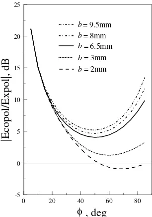
Fig. 1.18 shows the ratio Ecopol/Expol as a function of φ for different probe displacements. It is seen that the cross-polarisation level increases with decreasing
b. This is because, when b is small, stronger TM but weaker TE modes are excited, reducing the Ecopol/Expol ratio. Therefore, if polarisation purity is of primary
concern, the probe should be placed as near the edge of the DRA as possible, although in this case a pure resistance for proper impedance matching cannot be obtained [36].
It was found that the ratio Ecopol/Expol remains almost unchanged when the probe length l is varied, so the probe length can be used to vary the input impedance without the need to worry about increases in the cross-polarisation level.
Fig. 1.17 The ratio Ecopol/Expol versus φ for different dielectric constants: a = 12.5
mm, l = 6.5 mm, b = 6.5 mm, r1 = 0.5 mm, r2 = 1 mm. (From [51], © 1999
IEEE)
0 20 40 60 80 100 -30
-20 -10 0 10 20
, deg
|Eco
po
l/Exp
ol|
, dB
εr=20
9.5 4
2
1.002
Fig. 1.18 The ratio Ecopol/Expol versus φ for different probe displacements: a = 12.5
mm, l = 6.5 mm, r1 = 0.5 mm, r2 = 1 mm, εr = 9.5 and f = 3.68 GHz. (From
[51], © 1999 IEEE)
1.5 APERTURE-COUPLED DRA WITH A THICK GROUND PLANE
Thus far, the aperture-coupling excitation method with a microstrip feedline has been commonly used for the DRA. First, it allows a direct integration with active circuitry [53] and, second, it separates the DRA and feed network from one another. Most of the studies have concentrated on the case where the ground plane is infinitesimally thin. Sometimes, however, a thick ground plane is required to serve as a heat sink for active components. In other cases, the thick ground plane may be used as a mechanical support for thin substrates. Leung et al. [54] investigated the aperture-coupled hemispherical DRA with a thick ground plane. The DRA, as usual, is excited in the fundamental broadside TE111 mode.
The DRA configuration is shown in Fig. 1.19, where for ease of formulation, the DRA is shown beneath the thick ground plane. The slot of length L and width
W is located at the center of the DRA to obtain the strongest coupling [55]. Let My1 and My2 be the equivalent magnetic currents at the upper and lower
interfaces of the slot, respectively. Then by enforcing the boundary condition that the tangential magnetic field is continuous across each of the apertures, we have
Fig. 1.19 Geometry of the DRA with a thick ground plane. (From [54], © 1998
where
H
yf is the magnetic field caused by the feedline current. The superscriptsa, b, c, and s denote the fields at their corresponding interfaces in Fig. 1.19, and bc
(cb) denotes the field at surface b (c) due to the magnetic current at surface c (b). Using the MoM, the magnetic currents are expanded for i = 1, 2,as
where t denotes the transpose of a matrix, ∆vm is associated with the feedline field,
and
Y
mna andY
mns are the DRA and substrate admittances, respectively. All of these quantities are given in [55]. Other admittances αmn
respectively. The sign in (1.57) is determined by that of the magnetic current in (1.52). Note that the Green’s function
G
cy has only one summation and is independent of x. This implies thatG
cy contains only TE0l modes, which is a validapproximation for a narrow slot (or waveguide). After the magnetic currents are obtained, the input impedance and the radiation fields can be found easily.
slot now acts as a waveguide below cutoff. Thus, the energy transferred to the DRA is solely through evanescent waves, which attenuate quickly as t increases.
Fig. 1.20 Input impedance of the DRA for t = 0.0187, 0.4, and 0.8 mm: r = 12.5 mm, εra = 9.5, L = 11.8 mm, W = 1.0 mm, d = 1.58 mm, εrs = 2.33, Wf = 4.68
mm, and Ls = 11.5 mm. (From [54], © 1998 IEEE) Theory, Experiment;
: 3.30GHz, ∇ : 3.55GHz (Theory), : 3.55GHz (Exp.), ∆ : 3.90 GHz.
Fig. 1.21 shows the measured and calculated peak resistances as a function of the ratio t/λ0, where λ0 (= 86.7 mm) is the resonant wavelength in vacuum for t =
0.0187 mm. It is seen that excellent agreement between theory and experiment is obtained. The coupling decays quickly when t is small, and it approaches the one-way attenuation rate of the TE01 waveguide (slot) mode as t increases. A similar
phenomena has been discovered and explained in the study of the microstrip antenna version [56]. Also shown in the figure are the measured and calculated resonant frequencies (peak-resistance point) as a function of t/λ0. Good agreement
Fig. 1.21 Input resistance and resonant frequency of the DRA versus the normalised thickness t/λ0. The parameters are the same as Fig. 1.20. (From [54], ©
1998 IEEE)
1.6 SIMPLE RESULTS FOR THE SLOT-COUPLED HEMISPHERICAL DRA
As mentioned previously, slot coupling is often used for the DRA. Using the Green’s function technique together with the MoM, a quadruple integral naturally results for the DRA part. Although the quadruple integral can be reduced to a double integral by taking the narrow-slot approximation (kW << 1, W << L), numerical calculations of the double integral still require substantial computation time and programming effort. Based on the single-mode theory [35], a computationally efficient formula for the integral can be obtained when the slot is at the center of the hemispherical DRA [57].
Fig. 1.22 shows the geometry of a slot-coupled DRA. Only the region that contains the DRA is considered here, and the actual excitation of the slot is not considered. Taking the single-mode approximation from the rigorous Green’s function of Hy [55], we have
2
surface. Using the MoM, the equivalent magnetic current is expanded as
∑
where fn(z) is the piecewise sinusoidal (PWS) basis function given by (1.55) with i
= 2. For convenience, the subscript i of (1.55) is dropped hereafter.
Fig. 1.22 The geometry of a slot coupled DRA.
The unknown voltage coefficients Vn’s are solved via the following matrix
equation
and Im is associated with the actual excitation of the configuration. In (1.64), the
factor of “−2” has been added to the integrals. The factor of two accounts for the ground plane effect, whereas the minus sign ensures that the tangential E-field is continuous across the slot. For the general case
Y
mnH must be calculated usingnumerical integration, but it is found that for a narrow slot,
Y
mnH can be given by the following expression:)
Note that
Y
mnH can now be calculated easily and quickly without the need for any numerical integration. ForY
mnP , no simple results are available and numerical integration must be used.To verify the theory, the previously calculated and measured results of the aperture-coupled DRA using a microstrip feedline [55] are used. This comparison is shown in Fig. 1.23, where excellent agreement between the present and previous theories is obtained.
It should be mentioned that although the result starts with the single-mode theory, it can be used for a rather wide frequency range - from extremely low frequencies (virtually dc) to frequencies below the resonance of the TE3m1 mode.
Note that as the TE2m1 mode cannot be excited for this particular slot position, the
Fig. 1.23 Input impedance of the slot-coupled hemispherical dielectric resonator antenna (microstrip-feedline). The DRA has radius a = 12.5 mm and dielectric constant εra = 9.5. The microstrip feedline has width Wf = 1.45
mm, printed on a substrate of dielectric constant εrs = 2.96 and thickness d =
0.635 mm. It has an open-circuited stub length of Ls = 13.6 mm from the center of the slot. The slot is placed at the center of the DRA. Solid line: rigorous theory, dots: simplified theory, dashed line: experiment.
1.7 LOW-PROFILE AND SMALL DRAs
Usually, the DRA is made of a dielectric material witha low permittivity (εr < 40)
to enhance the radiation. In 1994, Mongia et al. demonstrated the radiation properties of a low-profile rectangular DRA with a very high permittivity (εr =
100) [58]. An excellent impedance match was obtained with ~3 % impedance bandwidth. Latter, low-profile, high-permittivity circular [59] and triangular [60] DRAs were investigated and similar results were obtained. Esselle studied the low-profile DRA of low-permittivity (εr = 10.8) [61], and its feasibility was also
was reduced roughly by one half. Tam and Murch [65] extended the method for the annular sector DRA, details of which can be found in Chapter 7.
1.8 BROADBAND DRAs
Bandwidth enhancement techniques for the DRA have been a popular topic. It was first done in 1989 by Kishk et al. [66], who stacked two different DRAs on top of one another. Since the DRAs had different resonant frequencies, the configuration had a dual-resonance operation, broadening the antenna bandwidth. Sangiovanni et al. [67] employed the stacking method with three DRAs to further increase the antenna bandwidth. Leung et al. [68] introduced an air gap between the stacking and active DRA elements. They used a high-permittivity, low-profile DR as the stacking element, and good results were obtained. Junker et al. [69] analyzed the stacking configuration that employs a conducting or high-εr loading disk. Simon
and Lee [70] used another method in which two parasitic DRs were placed beside the DRA to increase the impedance bandwidth. Alternatively, Leung et al. [71] used the dual-disk method to enhance the bandwidth of the low-profile DRA of very high permittivity.
The above methods require extra DR elements. Some bandwidth-enhancement techniques are based on single-DRA configurations. For example, Wong et al. [72] introduced an air gap inside a hemispherical DRA to widen the impedance bandwidth. Ittipiboon et al. [73] performed a similar work with the rectangular DRA. Shum and Luk [74] placed an air gap between the DRA and ground plane to broaden the impedance bandwidth. Leung [75] investigated the case where the air gap inside the DRA is replaced by a conductor. Chen et al. [76] added a dielectric coating to the DRA to increase the impedance bandwidth. Similarwork was also carried out by Shum and Luk [77]. Lately, a parasitic conducting patch has been used to increase the impedance bandwidth of the DRA [78, 79]. The new method does not require any extra DR elements nor special DRAs and, hence, should facilitate designs of broadband DRAs.
The expanded work for the broadband hemispherical DRA can be found in Chapter 3, whereas that for the broadband rectangular- and cylindrical-DRAs is given in Chapter 5.
1.9 CIRCULARLY POLARISED DRAs
For a long time, studies DRAs have concentrated on those producing linearly polarisation (LP). Sometimes, however, systems using circular polarisation (CP) are preferred because they are insensitive to the transmitter and receiver orientations. In some applications, such as satellite communications, it also offers less sensitivity to propagation effects. In contrast, an LP signal cannot be received properly when the transmitter is orthogonal to the received field. Consequently, more effort has been devoted to the CP DRA in recent years.
[82-84]. The quadrature feeding method gives a wide axial ratio (AR) bandwidth, but it substantially increases the size and complexity of the feed network.
A single feedpoint can be used if a few percent of AR bandwidth is sufficient for the application. The basic principle of this approach is to excite two nearly degenerate orthogonal modes with space-time quadrature. For example, Petosa et al. [85] employed a cross-shaped slot-coupled DRA to excite CP fields. Alternatively, Oliver et al. [86] and Esselle [87] used a conventional rectangular DRA, with the coupling slot inclined at 450 with respect to the DRA to obtain a CP DRA. The method, however, cannot be applied to a DRA with a circular circumference (e.g., cylindrical or hemispherical). These geometries can, however, be attacked by using a cross-slot, as demonstrated by Huang et al. [88]. A CP excitation method that utilised a pair of parasitic conducting strips was proposed by Lee et al. [89]. Leung and Ng [90, 91] and Long et al. [79] found that a single parasitic patch can also be used to excite CP fields. Recently, Leung and Mok [92] used a perturbed annular slot to excite a CP DRA. In this section, the work of Leung and Mok is shown as an example for the CP DRA.
Fig. 1.24 shows the antenna configuration of the annular-slot excited CP cylindrical DRA. The annular slot is perturbed by two opposing stubs located at 45o and 225o from the x-axis. Each stub has width t and depth d. A hemispherical backing cavity of radius b is placed below the slot to eliminate undesirable backside radiation.
Fig. 1.24 The CP cylindrical DRA excited by the perturbed annular slot with a backing cavity. (a) Perspective view. (b) Perturbed annular slot with opposing stubs. (From [92], reprinted with permission from IEE)
A cylindrical DRA of a = 2 cm, h = 2 cm, and εr = 9.5 and a backing cavity of
b = 2.5 mm were used in [92]. Fig. 1.25(a) shows the measured return loss for different slot radii of r = 8, 10, and 12 mm, with W = 1 mm, t = 7, and d = 5 mm fixed. It is observed in the figure that an excellent impedance match is obtained at
Ground plane h
b y
x z
a
Annular slot with opposing stubs
Backing cavity
below ground plane Coaxial feed cable Cylindrical DRA
(a) (b)
r
W t
d
45o
y
the resonant frequency (min.
S
11 ) f = 1.96 GHz, which agrees reasonably well with the predicted value of 2.07 GHz (5% error) using the following design formula [93]: to account for the image effect of the ground plane. The corresponding ARs are shown in Fig. 1.25(b). It is found that an AR of 0.2 dB is obtained at f = 1.92 GHz, which is very close to the resonant frequency (1.96 GHz), as desired. The 3-dB axial ratio bandwidth is 3.4 %, which is typical for a singly fed CP DRA. Although it is seen in Fig. 1.25(a) that the input impedance can be changed by varying the slot radius, care has to be exercised, since the axial ratio will also change accordingly as is observed in Fig. 1.25(b).Fig. 1.25 Measured return loss and axial ratio against frequency for different slot radii: (a) Return loss; (b) Axial ratio. (From [92], reprinted with permission from IEE)
Fig. 1.26 shows the measured return loss and axial ratio for different stub depths of d = 3, 5, and 7 mm, with r = 12 mm and theother parameters unchanged. Again, the return loss and axial ratio are affected simultaneously, but the changes are much smaller in extent than in the previous case. Therefore, the stub depth can be used for fine-tuning in the final design. For the stub width t, it was found that its effect is even smaller than that of varying the stub depth.
Fig. 1.27 shows the measured y-z and x-z plane radiation patterns at resonance (f = 1.96 GHz) with r = 12 mm and d = 5 mm. Very good left-hand CP (LHCP) fields are obtained. The isolation between the right-hand CP (RHCP) and LHCP fields is at least 20 dB in the broadside direction (θ = 0o). Note that the radiation below the ground plane is due to the finite ground plane diffraction only, since the backside radiation of the slot is already blocked by the backing cavity. The measured antenna gain of the configuration with r = 12 mm and d = 5 mm is about 4.5 dBi around resonance, as shown in Fig. 1.28.
Fig. 1.26 Measured return loss and axial ratio against frequency for different stub depths. (a) Return loss; (b) Axial ratio. (From [92], reprinted with permission from IEE)
1.10 DRA ARRAYS
Since the antenna gain of a DRA is limited to ~5 dBi, different types of DRA arrays [94-99] have been studied for increasing the antenna gain. In this section, the array performance of the cylindrical DRA is demonstrated using 2×2 and 4×4 square arrays of aperture-coupled cylindrical DRAs. The designs start with the single-element DRA, whose configuration is shown in Fig. 1.29. The DRA has radius a = 5.96 mm, height h = 9.82 mm, and dielectric constant εra = 16. A
rectangular slot of length L = 8 mm and width W = 0.8 mm is located at the center of the DRA. The grounded dielectric slab has dielectric constant εrs = 2.33 and
thickness d = 1.57 mm, whereas the 50-Ω microstrip feedline has width Wf = 4.7
mm. An open stub of length Ls = 12 mm extends from the center of the slot.
1.6 1.7 1.8 1.9 2 2.1
0 2 4 6 8 10 12 14
Frequency (GHz) Axial Ratio (dB)
(a) (b)
d = 7 mm d = 5 mm d = 3 mm d = 7 mm
d = 5 mm d = 3 mm
1.7 1.8 1.9 2 2.1 2.2
-50 -40 -30 -20 -10 0
Fig. 1.27 Measured radiation patterns at f = 1.96 GHz. The parameters are the same as in Fig. 1.25 with r = 12 mm. (a) y-z plane; (b) x-z plane. (From [92], reprinted with permission from IEE)
Fig. 1.28 Measured antenna gain of the configuration. The parameters are the same as in Fig.1.25 with r = 12 mm. (From [92], reprinted with permission from
y-z plane x-z plane
(a) (b)
Fig.1.29 Geometry of the single element aperture-coupled cylindrical DRA.
Top views of the 2×2 and 4×4 DRA arrays are shown in Fig. 1.30. The spacing between adjacent array elements is D = 33.5 mm, which is one-half of the free-space wavelength at f = 4.46 GHz. Fig. 1.31 shows the photos of the 4×4 DRA array.
Fig. 1.30 4×4 and 2×2 DRA arrays.
y
x L Wf
Ls
W
microstrip feedline
slot
D=λο/2
D=λο/2 λ
g/4
(a)
(b)
Fig. 1.32 displays the measured return loss of the single-element, 2×2 subarray and 4×4 array. Because of the mutual coupling between array elements and fabrication tolerances, the resonant frequencies and bandwidths of the arrays deviate a bit from that of the single element. The results are summarised in Table 1.4, where the resonant frequency is defined as the minimum point of the return loss.
Fig. 1.32 Comparison of the measured return losses. Single element,
2×2 subarray, 4×4 array.
Resonant Frequency GHz
Min. Return Loss dB
Table 1.4 Summary of the return loss measurements.
Figs. 1.33-1.35 display the radiation patterns for the three cases. Obviously, the beamwidth decreases with increasing the number of array elements, as expected. The results of the radiation patterns are summarised in Table 1.5.
(a) E-plane (b) H-plane
Fig. 1.33 Measured radiation patterns of the single element.
4 4.2 4.4 4.6 4.8 5
Observation angle, deg
N
Observation angle, deg
(a) E-plane (b) H-plane Fig. 1.34 Measured radiation patterns of the 2×2 subarray.
(a) E-plane (b) H-plane
Fig. 1.35 Measured radiation patterns of the 4×4 array.
E-plane Field Pattern H-plane Field Pattern 3-dB
Table 1.5 Summary of the radiation patterncharacteristics.
Fig. 1.36 displays the overall comparison of the antenna gains for the single element, 2 × 2 subarray, and 4 × 4 array. The gain of the 4 × 4 array at its resonant frequency (4.56 GHz) is about 16 dBi, which is 5.2 dBi and 11.2 dBi higher than those of the 2 × 2 subarray and single element, respectively. Note that the gains are near their maximum values around the resonances, which is to be expected.
c opolarised
Observation angle, deg
N
Obs ervation angle, deg
Fig. 1.36 Measured antenna gains. single element, 2×2 subarray, 4×4 subarray.
Early radar installations were not very efficient due to the slow rotational speeds of their massive antennas. Even though smaller antenna sizes and lighter materials have been employed, rotational speed limitations still restrict the scanning rate of the antenna. The problem can be solved by using a phased array antenna, where each element is fed with a differently phased signal, such that the angle of the main lobe changes in response to the phase of the current. Thus, the antenna can be motionless while the direction of maximum radiationis changed. Leung et al. [96] have investigated the input impedance of the cylindrical DRA element when it is operated in an infinite phased array environment, as illustrated in Fig. 1.37(a). For measurements, the infinite phased array environment can be simulated using a waveguide simulator technique [100], as shown in Fig. 1.37(b). In [96], the equivalent array element spacing Dx and Dy were 28.8 and 29 mm,
respectively. The waveguide simulator effectively scans in the H-plane to an angle θ, where sinθ = λo/(4Dy). The waveguide simulator, covering the DR element, was
put on a grounded dielectric slab. Through mirror images formed inside the waveguide simulator, there are infinite numbers of DRA elements in different directions, forming an infinite DRA phased array environment. For measurements, the waveguide simulator supports the TE10 waveguide mode only.
The measured return loss of the simulator is displayed in Fig. 1.38. The scan angle of the waveguide simulation is also shown in the same figure, where it is seen that as frequency increases from 4 to 5GHz, the scan angle of the waveguide simulator decreases from 40.3o to 31.1o. It also shows that the resonant frequency
of the phased array is 4.57GHz, corresponding to a scan angle of 34.5o. Because of the mutual coupling between the array elements, the resonant frequency of the infinite array has shifted 2.5% from that of the single element (4.46GHz).
4 4.2 4.4 4.6 4.8 5
-5 0 5 10 15 20
F requency, GHz
G
a
in,
dB