ABSTRAK
Teknik pengendalian terus berkembang mengikuti laju perkembangan
teknologi yang saat ini menuntut adanya ketepatan dan kecepatan yang semakin
tinggi. Untuk masalah pemboran kedalaman, akan terasa sulit dilakukan secara
manual jika adanya permintaan yang banyak dan kedalaman yang ingin dibor
berbeda-beda. Dalam Tugas Akhir ini telah dirancang dan direalisasikan sebuah
alat pemboran dengan kedalaman yang diinginkan menggunakan mikrokontroler.
Alat pemboran kedalaman ini dirancang dan direalisasikan dengan
memanfaatkan modul sensor inframerah GP2D02, motor DC, papan ketik, dan
LCD yang dikendalikan oleh pengendali mikro PIC16F84. Masukan diberikan
melalui penekanan tombol papan ketik. Penekanan tombol ‘*’ untuk memasukkan
data panjang mata bor dan kedalaman yang diinginkan. Data masukan berupa dua
digit angka desimal dalam satuan cm. Penekanan tombol ‘#’ untuk menjalankan
proses pemboran. Motor DC akan menurunkan mesin bor sampai pada nilai
setpoint tertentu. Setelah nilai setpoint tercapai, motor DC segera menaikkan
mesin bor pada kedudukan semula. Dengan demikian, proses pemboran selesai
dan menunggu masukan data yang baru.
Pengujian kinerja alat pemboran kedalaman dilakukan dengan cara
melakukan pemboran terhadap kayu lunak (Borneo) dan kayu keras (Kamper).
Persentase kesalahan rata-rata pemboran terhadap kayu Borneo menggunakan
panjang mata bor 10 cm diameter 4,5 mm adalah 9,54 %, menggunakan panjang
mata bor 8 cm diameter 5 mm adalah 9,64 %, menggunakan panjang mata bor 6
cm diameter 6,5 mm adalah 25,10 %. Sedangkan persentase kesalahan pemboran
terhadap kayu Kamper menggunakan panjang mata bor 10 cm diameter 4,5 mm
adalah 9,99 %, menggunakan panjang mata bor 8 cm 5 mm adalah 9,88 %,
menggunakan panjang mata bor 6 cm diameter 6,5 mm adalah 25,34 %.
Kesalahan disebabkan karena adanya daerah mati (
deadzone
) pada sistem
Control technique non-stopped to expand to follow fast of technology
growth which in this time claim the existence of accuracy and speed which
excelsior. For the problem of deepness drilling, will be felt done difficult in
manual of if existence of request which is a lot of and deepness which wish drilled
different each other. In this Final Duty have been designed and realized by a
drilling appliance with the deepness wanted use the microcontroller.
This deepness Drilling appliance is designed and realized by exploiting
infra-red censor module of GP2D02, motor DC, board type, and LCD controlled
by micro controller of PIC16F84. Input given by through emphasis of board knob
type the. Knob emphasis '*' to enter the long data of eye drill and wanted
deepness. Input data in the form of two number digit denary in set of cm. Knob
emphasis '#' to run process the drilling. Motor DC will degrade the drilling
machine come up with the certain value set point. After value set point reached
the, motor DC immediately boost up the drilling machine at domiciling from the
beginning. Thereby, process the drilling to finish and await the new data input.
DAFTAR ISI
Halaman
ABSTRAK
………. i
ABSTRACT ……… ii
KATA PENGANTAR……….. iii
DAFTAR ISI ………...
v
DAFTAR GAMBAR……… viii
DAFTAR TABEL………
ix
BAB I PENDAHULUAN
I.1 Latar Belakang Masalah……….…... 1
I.2 Identifikasi Masalah……….. 2
I.3 Tujuan………... 2
I.4 Pembatasan Masalah………. 2
I.5 Sistem Pembahasan……….. 3
BAB II TEORI PENUNJANG
II.1 Mikrokontroler PIC16F84……… 4
II.1.1 Deskripsi Pin-pin………. 6
II.1.2 Organisasi Memori……….. 8
II.1.2.1 Organisasi Memori Program……….. 9
II.1.2.2 Organisasi Memori Data………... 10
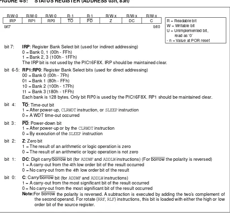
II.1.3 Register Fungsi Khusus………... 11
II.1.3.1 Register STATUS……….. 12
II.1.3.2 Register OPTION_REG………. 13
II.1.3.3 Register INTCON………...….14
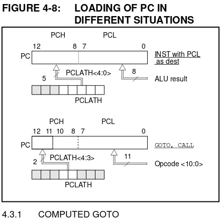
II.1.3.4 Program Counter, PCL, dan PCLATCH………… 15
II.1.3.5 Stack………... 15
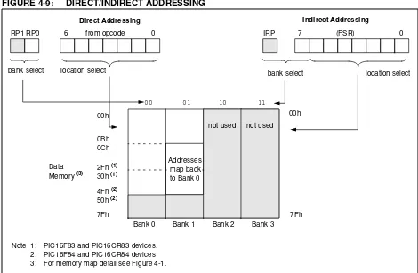
II.1.3.6 Pengalamatan Tak Langsung………... 16
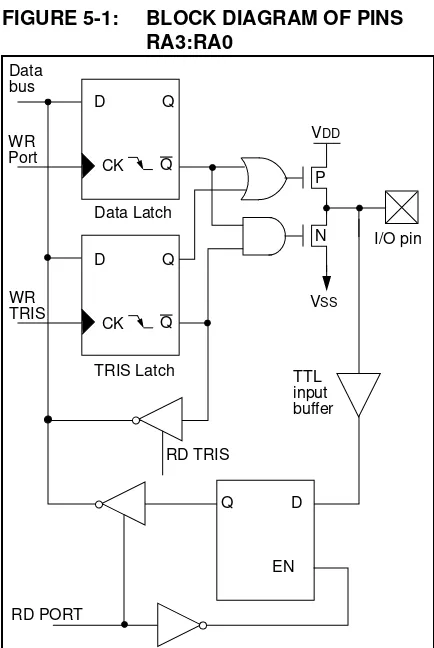
II.1.5 Port Masukan/Keluaran………... 18
II.1.5.1 Register PORTA dan TRISA………. 18
II.1.5.2 Register PORTB dan TRISB………..19
II.1.6 Pewaktu………... 21
II.1.6.1 Modul TIMER0 dan Register TMR0………. 22
II.1.6.2 Pewaktu Power-up………..22
II.1.6.3 Pewaktu Start-up Osilator (OST)………... 23
II.1.6.4 Pewaktu Watchdog (WDT)……… 23
II.1.6.5 Penyekala………24
II.1.7 Memori Data EEPROM……….. 24
II.1.7.1 Register EECON1 dan EECON2………... 24
II.1.7.2 Register EEDATA dan EEADR……….25
II.1.8 Reset……… 25
II.1.9 Interupsi………..…….26
II.1.9.1 Interupsi Eksternal RB0/INT………..……..27
II.1.9.2 Interupsi TMR0……….. 27
II.1.9.3 Interupsi PORTB……… 27
II.1.10 Set Instruksi………... 27
II.1.11 Format Instruksi……… 29
II.1.12 Register Fungsi Khusus sebagai Sumber/Tujuan……….. 31
II.2 Pengendali Motor DC………….………..33
II.3 Modul Sensor Inframerah GP2D02………. 35
BAB III PERANCANGAN DAN REALISASI
III.1 Diagram Kerja dan Cara Kerja…..………. 39
III.2 Sistem Mekanik……….. 41
III.3 Perancangan Perangkat keras Internal……… 42
III.3.1 Rangkaian Antarmuka PIC16F84 dengan Modul
Sensor Inframerah ………..…. 42
III.3.2 Rangkaian Secara Keseluruhan………..…. 43
III.4 Perancangan Perangkat Keras Eksternal……….44
III.4.2 Perancangan Rangkaian Pengatur Kecepatan
Motor DC………... 45
III.4.3 Perancangan Rangkaian Penggerak Relai…………..…. 46
III.5 Perancangan Perangkat Lunak……… 47
III.5.1 Subprogram untuk Pembacaan Modul Sensor
Inframerah ……….. 47
III.5.2 Program Keseluruhan………... 47
BAB IV PENGUJIAN DAN ANALISA KINERJA ALAT
IV.1 Pengujian Rangkaian Antarmuka PIC16F84 dengan
Modul Sensor Inframerah………...…… 51
IV.2 Pengujian Rangkaian Catu Daya……… 61
IV.3 Pengujian Alat Secara Keseluruhan………... 62
IV.3.1 Pengujian Terhadap Kayu Lunak (Borneo)…………
62
IV.3.1.1 Pengujian dengan Panjang Mata Bor 10 cm….. 62
IV.3.1.2 Pengujian dengan Panjang Mata Bor 8 cm…… 62
IV.3.1.3 Pengujian dengan Panjang Mata Bor 6 cm…… 63
IV.3.2 Pengujian Terhadap Kayu Keras (Kayu Kamper)……... 63
IV.3.1.1 Pengujian dengan Panjang Mata Bor 10 cm….. 63
IV.3.1.2 Pengujian dengan Panjang Mata Bor 8 cm…… 63
IV.3.1.3 Pengujian dengan Panjang Mata Bor 6 cm…… 63
BAB V KESIMPULAN DAN SARAN
V.1 Kesimpulan………...72
V.2 Saran……….73
DAFTAR PUSTAKA
LAMPIRAN A. Foto Alat
B. Rangkaian Keseluruhan
C. Perangkat Lunak
DAFTAR GAMBAR
Gambar 2.1
Pin-pin Mikrokontroler PIC16F84
Gambar 2.2
Peta Memori Program dan Stack PIC16F83/CR83
Gambar 2.3
Peta Memori Program dan Stack PIC16F84/CR84
Gambar 2.4
Peta File Register PIC16F83/CR83
Gambar 2.5
Peta File Register PIC16F84/CR84
Gambar 2.6
Pengoperasian Osilator Kristal (Konfigurasi LP, XT, HS)
Gambar 2.7
Tegangan Keluaran Multivibrator Astabil
Gambar 2.8
Rangkaian Multivibrator Astabil
Gambar 2.9
LED Pemancar Inframerah
Gambar 2.10
Position Sensitive Detector (PSD)
Gambar 2.11
Struktur Position Sensitive Photodioda
Gambar 2.12
Cara Kerja Modul Sensor GP2D02
Gambar 2.13
Diagram Pewaktuan Pengukuran dan Keluaran Data
Gambar 3.1
Diagram Kerja Alat Pemboran Kedalaman
Gambar 3.2
Rancangan Alat Pemboran Kedalaman
Gambar 3.3
Rangkaian Antarmuka PIC16F84 dengan Modul Sensor
Gambar 3.4
Rangkaian Catu Daya 5 Volt
Gambar 3.5
Rangkaian Catu Daya 12 Volt
Gambar 3.6
Rangkaian Pengaturan Kecepatan Motor DC
Gambar 3.7
Flowchart Subprogram untuk Pembacaan Sensor
DAFTAR TABEL
Tabel 2.1
Fungsi Pin-pin pada PIC16X8X
Tabel 2.2
Perbandingan Keluarga PIC16X8X
Tabel 2.3
Piranti Keluarga PIC16X8X
Tabel 2.4
Register STATUS (Alamat 03h, 83h)
Tabel 2.5
Register OPTION_REG (Alamat 81h)
Tabel 2.6
Register INTCON (Alamat 0Bh, 8Bh)
Tabel 2.7
Tipikal Pemilihan Nilai Kapasitor untuk Osilator Kristal
Tabel 2.8
Fungsi Port A
Tabel 2.9
Fungsi Port B
Tabel 2.10
Uraian Bidang Opcode
Tabel 2.11
Format Umum untuk Instruksi
Tabel 2.12
Set Instruksi PIC16F8X
Tabel 4.1
Hasil Pembacaan Modul Sensor Inframerah
Tabel 4.2
Hasil Pengukuran Tegangan Keluaran Catu Daya
Tabel 4.3
Hasil Pengujian Terhadap Kayu Borneo dengan Panjang
Mata
Bor
10
cm
Tabel 4.4
Hasil Pengujian Terhadap Kayu Borneo dengan Panjang
Mata
Bor
8
cm
Tabel 4.5
Hasil Pengujian Terhadap Kayu Borneo dengan Panjang
Mata
Bor
6
cm
Tabel 4.6
Hasil Pengujian Terhadap Kayu Kamper dengan Panjang
Mata
Bor
10
cm
Tabel 4.7
Hasil Pengujian Terhadap Kayu Kamper dengan Panjang
Mata
Bor
8
cm
Tabel 4.8
Hasil Pengujian Terhadap Kayu Kamper dengan Panjang
Mata
Bor
6
cm
Tabel 4.9
Persentase Kesalahan Rata-Rata Hasil Pemboran
DATA SHEET
Product specification
Supersedes data of 1998 Jun 04
2003 Jun 25
INTEGRATED CIRCUITS
74HC595; 74HCT595
Philips Semiconductors Product specification
8-bit serial-in, serial or parallel-out shift
register with output latches; 3-state
74HC595; 74HCT595
FEATURES
• 8-bit serial input
• 8-bit serial or parallel output
• Storage register with 3-state outputs
• Shift register with direct clear
• 100 MHz (typical) shift out frequency
• ESD protection:
HBM EIA/JESD22-A114-A exceeds 2000 V MM EIA/JESD22-A115-A exceeds 200 V.
APPLICATIONS
• Serial-to-parallel data conversion
• Remote control holding register.
DESCRIPTION
The 74HC/HCT595 are high-speed Si-gate CMOS devices and are pin compatible with low power Schottky TTL (LSTTL). They are specified in compliance with JEDEC standard no. 7A.
The 74HC/HCT595 is an 8-stage serial shift register with a storage register and 3-state outputs. The shift register and storage register have separate clocks.
Data is shifted on the positive-going transitions of the SH_CP input. The data in each register is transferred to the storage register on a positive-going transition of the ST_CP input. If both clocks are connected together, the shift register will always be one clock pulse ahead of the storage register.
The shift register has a serial input (DS) and a serial standard output (Q7’) for cascading. It is also provided with asynchronous reset (active LOW) for all 8 shift register stages. The storage register has 8 parallel 3-state bus driver outputs. Data in the storage register appears at the output whenever the output enable input (OE) is LOW.
QUICK REFERENCE DATA
GND = 0 V; Tamb= 25°C; tr= tf= 6 ns.
Notes
1. CPD is used to determine the dynamic power dissipation (PDinµW). PD= CPD×VCC2×fi×N +Σ(CL×VCC2×fo) where:
fi= input frequency in MHz; fo= output frequency in MHz; CL= output load capacitance in pF; VCC= supply voltage in Volts; N = total load switching outputs;
Σ(CL×VCC2×fo) = sum of the outputs.
2. For 74HC595 the condition is VI= GND to VCC.
−
SYMBOL PARAMETER CONDITIONS TYPICAL UNIT
74HC 74HCT
tPHL/tPLH propagation delay CL= 50 pF; VCC= 4.5 V
SH_CP to Q7’ 19 25 ns
SH_CP to Qn 20 24 ns
MR to Q7’ 100 52 ns
fmax maximum clock frequency SH_CP and ST_CP 100 57 MHz
CI input capacitance 3.5 3.5 pF
2003 Jun 25 3
8-bit serial-in, serial or parallel-out shift
register with output latches; 3-state
74HC595; 74HCT595
FUNCTION TABLE
See note 1.
Note
1. H = HIGH voltage level; L = LOW voltage level;
↑= LOW-to-HIGH transition;
↓= HIGH-to-LOW transition; Z = high-impedance OFF-state; n.c. = no change;
X = don’t care.
ORDERING INFORMATION
INPUT OUTPUT
FUNCTION SH_CP ST_CP OE MR DS Q7’ Qn
X X L L X L n.c. a LOW level on MR only affects the shift registers
X ↑ L L X L L empty shift register loaded into storage register
X X H L X L Z shift register clear; parallel outputs in high-impedance
OFF-state
↑ X L H H Q6’ n.c. logic high level shifted into shift register stage 0;
contents of all shift register stages shifted through, e.g. previous state of stage 6 (internal Q6’) appears on the serial output (Q7’)
X ↑ L H X n.c. Qn’ contents of shift register stages (internal Qn’) are
transferred to the storage register and parallel output stages
↑ ↑ L H X Q6’ Qn’ contents of shift register shifted through; previous
contents of the shift register is transferred to the storage register and the parallel output stages
TYPE NUMBER
PACKAGE
TEMPERATURE
RANGE PINS PACKAGE MATERIAL CODE
74HC595N −40 to +125°C 16 DIP16 plastic SOT38-4
74HCT595N −40 to +125°C 16 DIP16 plastic SOT38-4
74HC595D −40 to +125°C 16 SO16 plastic SOT109-1
74HCT595D −40 to +125°C 16 SO16 plastic SOT109-1
74HC595DB −40 to +125°C 16 SSOP16 plastic SOT338-1
74HCT595DB −40 to +125°C 16 SSOP16 plastic SOT338-1
74HC595PW −40 to +125°C 16 TSSOP16 plastic SOT403-1
74HCT595PW −40 to +125°C 16 TSSOP16 plastic SOT403-1
74HC595BQ −40 to +125°C 16 DHVQFN16 plastic SOT763-1
Philips Semiconductors Product specification
8-bit serial-in, serial or parallel-out shift
register with output latches; 3-state
74HC595; 74HCT595
PINNING
PIN SYMBOL DESCRIPTION
1 Q1 parallel data output
2 Q2 parallel data output
3 Q3 parallel data output
4 Q4 parallel data output
5 Q5 parallel data output
6 Q6 parallel data output
7 Q7 parallel data output
8 GND ground (0 V)
9 Q7’ serial data output
10 MR master reset (active LOW)
11 SH_CP shift register clock input
12 ST_CP storage register clock input
13 OE output enable (active LOW)
14 DS serial data input
15 Q0 parallel data output
16 VCC positive supply voltage
handbook, halfpage Q1 Q2 Q3 Q4 Q5 Q6 Q7 Q7' Q0 DS GND ST_CP SH_CP VCC OE 1 2 3 4 5 6 7 8 16 15 14 13 12 11 10 9 595 MLA001 MR
Fig.1 Pin configuration DIP16, SO16 and (T)SSOP16. handbook, halfpage 1 16 GND(1) Q1 VCC 8 2 3 4 5 7 Q2 Q3 Q4 Q5 Q6 15 14 13 12 10 6 11 9 GND
Top view MBL893
Q7 Q7' MR SH_CP ST_CP OE DS Q0
Fig.2 Pin configuration DHVQFN16. (1) The die substrate is attached to this pad using conductive die
2003 Jun 25 5
8-bit serial-in, serial or parallel-out shift
register with output latches; 3-state
74HC595; 74HCT595
handbook, halfpage OE MR 9 15 1 2 3 4 5 6 7 13 10 14 11 12 MLA002 Q1 Q0 Q2 Q3 Q4 Q5 Q6 Q7 Q7' DS ST_CP SH_CP
Fig.3 Logic symbol.
handbook, halfpage MSA698 15 9 1 2 3 4 5 6 7 1D 2D C1/ 10 11 14 C2 12 13 EN3 SRG8 R 3 OE MR Q1 Q0 Q2 Q3 Q4 Q5 Q6 Q7 Q7' DS ST_CP SH_CP
Fig.4 IEC logic symbol.
handbook, full pagewidth
ST_CP DS SH_CP
MR
Q7' 8-STAGE SHIFT REGISTER
8-BIT STORAGE REGISTER 14 11 10 12 9 OE 3-STATE OUTPUTS Q1 Q2 Q3 Q5 Q6 Q7 Q4 Q0 15 1 2 3 4 5 6 7 13 MLA003
Philips Semiconductors Product specification
8-bit serial-in, serial or parallel-out shift
register with output latches; 3-state
74HC595; 74HCT595
handbook, full pagewidth
STAGE 0 STAGES 1 to 6 STAGE 7
FF0 D
CP Q
R
LATCH D
CP Q
FF7 D
CP Q
R
LATCH D
CP Q
MLA010
D Q
Q1 Q2 Q3 Q4 Q5 Q6 Q7
Q7'
Q0 DS
ST_CP SH_CP
OE MR
2003 Jun 25 7
8-bit serial-in, serial or parallel-out shift
register with output latches; 3-state
74HC595; 74HCT595
handbook, full pagewidth
high-impedance OFF-state ST_CP
DS SH_CP
MR
OE
Q1 Q0
Q7' Q6
Q7
MLA005-1
Philips Semiconductors Product specification
8-bit serial-in, serial or parallel-out shift
register with output latches; 3-state
74HC595; 74HCT595
RECOMMENDED OPERATING CONDITIONS
LIMITED VALUES
In accordance with the Absolute Maximum Rating System (IEC 60134); voltages are referenced to GND (ground = 0 V).
Note
1. For DIP16 packages: above 70°C derate linearly with 12 mW/K. For SO16 packages: above 70°C derate linearly with 8 mW/K. For SSOP16 packages: above 60°C derate linearly with 5.5 mW/K. For TSSOP16 packages: above 60°C derate linearly with 5.5 mW/K. For DHVQFN16 packages: above 60°C derate linearly with 4.5 mW/K.
SYMBOL PARAMETER CONDITIONS 74HC 74HCT UNIT
MIN. TYP. MAX. MIN. TYP. MAX.
VCC supply voltage 2.0 5.0 6.0 4.5 5.0 5.5 V
VI input voltage 0 − VCC 0 − VCC V
VO output voltage 0 − VCC 0 − VCC V
Tamb ambient temperature −40 − +125 −40 − +125 °C
tr, tf input rise and fall time VCC= 2.0 V − − 1000 − − − ns
VCC= 4.5 V − 6.0 500 − 6.0 500 ns
VCC= 6.0 V − − 400 − − − ns
SYMBOL PARAMETER CONDITIONS MIN. MAX. UNIT
VCC supply voltage −0.5 +7.0 V
IIK input diode current VI<−0.5 V to VI> VCC+ 0.5 V − ±20 mA
IOK output diode current VO<−0.5 V to VO> VCC+ 0.5 V − ±20 mA
IO output source or sink current VO=−0.5 V to VCC+ 0.5 V
Q7’ standard output − ±25 mA
Qn bus driver outputs − ±35 mA
ICC, IGND VCC or GND current − ±70 mA
Tstg storage temperature −65 +150 °C
2003 Jun 25 9
8-bit serial-in, serial or parallel-out shift
register with output latches; 3-state
74HC595; 74HCT595
DC CHARACTERISTICS Type 74HC
At recommended operating conditions; voltages are referenced to GND (ground = 0 V).
SYMBOL PARAMETER TEST CONDITIONS MIN. TYP. MAX. UNIT OTHER VCC (V)
Tamb=−40 to +85°C; note 1
VIH HIGH-level input
voltage
2.0 1.5 1.2 − V
4.5 3.15 2.4 − V
6.0 4.2 3.2 − V
VIL LOW-level input
voltage
2.0 − 0.8 0.5 V
4.5 − 2.1 1.35 V
6.0 − 2.8 1.8 V
VOH HIGH-level output
voltage
VI= VIH or VIL all outputs
IO=−20µA 2.0 1.9 2.0 − V
4.5 4.4 4.5 − V
6.0 5.9 6.0 − V
Q7’ standard output
IO=−4.0 mA 4.5 3.84 4.32 − V
IO=−5.2 mA 6.0 5.34 5.81 − V
Qn bus driver outputs
IO=−6.0 mA 4.5 3.84 4.32 − V
IO=−7.8 mA 6.0 5.34 5.81 − V
VOL LOW-level output
voltage
VI= VIH or VIL all outputs
IO= 20µA 2.0 − 0 0.1 V
4.5 − 0 0.1 V
6.0 − 0 0.1 V
Q7’ standard output
IO= 4.0 mA 4.5 − 0.15 0.33 V
IO= 5.2 mA 6.0 − 0.16 0.33 V
Qn bus driver outputs
IO= 6.0 mA 4.5 − 0.16 0.33 V
IO= 7.8 mA 6.0 − 0.16 0.33 V
ILI input leakage current VI= VCCor GND 6.0 − − ±1.0 µA
IOZ 3-state output
OFF-state current
VI= VIHor VIL; VO= VCCor GND
6.0 − − ±5.0 µA
ICC quiescent supply
current
VI= VCCor GND; IO= 0
Philips Semiconductors Product specification
8-bit serial-in, serial or parallel-out shift
register with output latches; 3-state
74HC595; 74HCT595
Note
1. All typical values are measured at Tamb= 25°C.
Tamb=−40 to +125°C
VIH HIGH-level input
voltage
2.0 1.5 − − V
4.5 3.15 − − V
6.0 4.2 − − V
VIL LOW-level input
voltage
2.0 − − 0.5 V
4.5 − − 1.35 V
6.0 − − 1.8 V
VOH HIGH-level output
voltage
VI= VIH or VIL all outputs
IO=−20µA 2.0 1.9 − − V
4.5 4.4 − − V
6.0 5.9 − − V
Q7’ standard output
IO=−4.0 mA 4.5 3.7 − − V
IO=−5.2 mA 6.0 5.2 − − V
Qn bus driver outputs
IO=−6.0 mA 4.5 3.7 − − V
IO=−7.8 mA 6.0 5.2 − − V
VOL LOW-level output
voltage
VI= VIH or VIL all outputs
IO= 20µA 4.5 − − 0.1 V
Q7’ standard output
IO= 4.0 mA 4.5 − − 0.4 V
Qn bus driver outputs
IO= 6.0 mA 4.5 − − 0.4 V
ILI input leakage current VI= VCCor GND 5.5 − − ±1.0 µA
IOZ 3-state output
OFF-state current
VI= VIHor VIL; VO= VCCor GND
5.5 − − ±10.0 µA
ICC quiescent supply
current
VI= VCCor GND; IO= 0
5.5 − − 160 µA
2003 Jun 25 11
8-bit serial-in, serial or parallel-out shift
register with output latches; 3-state
74HC595; 74HCT595
Type 74HCT
At recommended operating conditions; voltages are referenced to GND (ground = 0 V); tr= tf= 6 ns; CL= 50 pF.
SYMBOL PARAMETER TEST CONDITIONS MIN. TYP. MAX. UNIT OTHER VCC (V)
Tamb=−40 to +85°C;note 1
VIH HIGH-level input
voltage
4.5 to 5.5 2.0 1.6 − V
VIL LOW-level input
voltage
4.5 to 5.5 − 1.2 0.8 V
VOH HIGH-level output
voltage
VI= VIHor VIL all outputs
IO=−20µA 4.5 4.4 4.5 − V
Q7’ standard output
IO=−4.0 mA 4.5 3.84 4.32 − V
Qn bus driver outputs
IO=−6.0 mA 4.5 3.7 4.32 − V
VOL LOW-level output
voltage
VI= VIHor VIL all outputs
IO= 20µA 4.5 − 0 0.33 V
Q7’ standard output
IO= 4.0 mA 4.5 − 0.15 0.33 V
Qn bus driver outputs
IO= 6.0 mA 4.5 − 0.16 0.33 V
ILI input leakage current VI= VCCor GND 5.5 − − ±1.0 µA
IOZ 3-state output
OFF-state current
VI= VIHor VIL; VO= VCCor GND
5.5 − − ±5.0 µA
ICC quiescent supply
current
VI= VCCor GND; IO= 0
5.5 − − 80 µA
∆ICC additional supply
current per input
VI= VCC−2.1 V; IO= 0; note 2
Philips Semiconductors Product specification
8-bit serial-in, serial or parallel-out shift
register with output latches; 3-state
74HC595; 74HCT595
Notes
1. All typical values are measured at Tamb= 25°C.
2. The value of additional quiescent supply current (∆ICC) for a unit load of 1 is given here. To determine∆ICCper input, multiply this value by the unit load coefficient per input pin:
a. pin DS: 0.25
b. pins MR, SH_CP, ST_CP and OE: 1.50.
Tamb=−40 to +125°C
VIH HIGH-level input
voltage
4.5 to 5.5 2.0 − − V
VIL LOW-level input
voltage
4.5 to 5.5 − − 0.8 V
VOH HIGH-level output
voltage
VI= VIHor VIL all outputs
IO=−20µA 4.5 4.4 − − V
Q7’ standard output
IO=−4.0 mA 4.5 3.7 − − V
Qn bus driver outputs
IO=−6.0 mA 4.5 3.7 − − V
VOL LOW-level output
voltage
VI= VIHor VIL all outputs
IO= 20µA 4.5 − − 0.1 V
Q7’ standard output
IO= 4.0 mA 4.5 − − 0.4 V
Qn bus driver outputs
IO= 6.0 mA 4.5 − − 0.4 V
ILI input leakage current VI= VCCor GND 5.5 − − ±1.0 µA
IOZ 3-state output
OFF-state current
VI= VIHor VIL; VO= VCCor GND
5.5 − − ±10.0 µA
ICC quiescent supply
current
VI= VCCor GND; IO= 0
5.5 − − 160 µA
∆ICC additional supply
current per input
VI= VCC−2.1 V; IO= 0; note 2
4.5 to 5.5 − − 490 µA
2003 Jun 25 13
8-bit serial-in, serial or parallel-out shift
register with output latches; 3-state
74HC595; 74HCT595
AC CHARACTERISTICS Family 74HC
GND = 0 V; tr= tf= 6 ns; CL= 50 pF.
SYMBOL PARAMETER TEST CONDITIONS MIN. TYP. MAX. UNIT WAVEFORMS VCC (V)
Tamb= 25°C
tPHL/tPLH propagation delay SH_CP to Q7’
see Fig.7 2.0 − 52 160 ns
4.5 − 19 32 ns
6.0 − 15 27 ns
propagation delay ST_CP to Qn
see Fig.8 2.0 − 55 175 ns
4.5 − 20 35 ns
6.0 − 16 30 ns
tPHL propagation delay
MR to Q7’
see Fig.10 2.0 − 47 175 ns
4.5 − 17 35 ns
6.0 − 14 30 ns
tPZH/tPZL 3-state output enable time OE to Qn
see Fig.11 2.0 − 47 150 ns
4.5 − 17 30 ns
6.0 − 14 26 ns
tPHZ/tPLZ 3-state output disable time OE to Qn
see Fig.11 2.0 − 41 150 ns
4.5 − 15 30 ns
6.0 − 12 26 ns
tW shift clock pulse width
HIGH or LOW
see Fig.7 2.0 75 17 − ns
4.5 15 6 − ns
6.0 13 5 − ns
storage clock pulse width HIGH or LOW
see Fig.8 2.0 75 11 − ns
4.5 15 4 − ns
6.0 13 3 − ns
master reset pulse width LOW
see Fig.10 2.0 75 17 − ns
4.5 15 6.0 − ns
6.0 13 5.0 − ns
tsu set-up time DS to SH_CP see Fig.9 2.0 50 11 − ns
4.5 10 4.0 − ns
6.0 9.0 3.0 − ns
set-up time SH_CP to ST_CP
see Fig.8 2.0 75 22 − ns
4.5 15 8 − ns
6.0 13 7 − ns
th hold time DS to SH_CP see Fig.9 2.0 +3 −6 − ns
4.5 +3 −2 − ns
Philips Semiconductors Product specification
8-bit serial-in, serial or parallel-out shift
register with output latches; 3-state
74HC595; 74HCT595
trem removal time MR to SH_CP see Fig.10 2.0 +50 −19 − ns
4.5 +10 −7 − ns
6.0 +9 −6 − ns
fmax maximum clock
pulse frequency SH_CP or ST_CP
see Figs 7 and 8 2.0 9 30 − MHz
4.5 30 91 − MHz
6.0 35 108 − MHz
Tamb=−40 to +85°C
tPHL/tPLH propagation delay SH_CP to Q7’
see Fig.7 2.0 − − 200 ns
4.5 − − 40 ns
6.0 − − 34 ns
propagation delay ST_CP to An
see Fig.8 2.0 − − 220 ns
4.5 − − 44 ns
6.0 − − 37 ns
tPHL propagation delay
MR to Q7’
see Fig.10 2.0 − − 220 ns
4.5 − − 44 ns
6.0 − − 37 ns
tPZH/tPZL 3-state output enable time OE to Qn
see Fig.11 2.0 − − 190 ns
4.5 − − 38 ns
6.0 − − 33 ns
tPHZ/tPLZ 3-state output disable time OE to Qn
see Fig.11 2.0 − − 190 ns
4.5 − − 38 ns
6.0 − − 33 ns
tW shift clock pulse width
HIGH or LOW
see Fig.7 2.0 95 − − ns
4.5 19 − − ns
6.0 16 − − ns
storage clock pulse width HIGH or LOW
see Fig.8 2.0 95 − − ns
4.5 19 − − ns
6.0 16 − − ns
master reset pulse width LOW
see Fig.10 2.0 95 − − ns
4.5 19 − − ns
6.0 16 − − ns
tsu set-up time DS to SH_CP see Fig.9 2.0 65 − − ns
4.5 13 − − ns
6.0 11 − − ns
set-up time SH_CP to ST_CP
see Fig.8 2.0 95 − − ns
4.5 19 − − ns
6.0 16 − − ns
2003 Jun 25 15
8-bit serial-in, serial or parallel-out shift
register with output latches; 3-state
74HC595; 74HCT595
th hold time DS to SH_CP see Fig.9 2.0 3 − − ns
4.5 3 − − ns
6.0 3 − − ns
trem removal time MR to SH_CP see Fig.10 2.0 65 − − ns
4.5 13 − − ns
6.0 11 − − ns
fmax maximum clock
pulse frequency SH_CP or ST_CP
see Figs 7 and 8 2.0 4.8 − − MHz
4.5 24 − − MHz
6.0 28 − − MHz
Tamb=−40 to +125°C
tPHL/tPLH propagation delay SH_CP to Q7’
see Fig.7 2.0 − − 240 ns
4.5 − − 48 ns
6.0 − − 41 ns
propagation delay ST_CP to Qn
see Fig.8 2.0 − − 265 ns
4.5 − − 53 ns
6.0 − − 45 ns
tPHL propagation delay
MR to Q7’
see Fig.10 2.0 − − 265 ns
4.5 − − 53 ns
6.0 − − 45 ns
tPZH/tPZL 3-state output enable time OE to Qn
see Fig.11 2.0 − − 225 ns
4.5 − − 45 ns
6.0 − − 38 ns
tPHZ/tPLZ 3-state output disable time OE to Qn
see Fig.11 2.0 − − 225 ns
4.5 − − 45 ns
6.0 − − 38 ns
tW shift clock pulse width
HIGH or LOW
see Fig.7 2.0 110 − − ns
4.5 22 − − ns
6.0 19 − − ns
storage clock pulse width HIGH or LOW
see Fig.8 2.0 110 − − ns
4.5 22 − − ns
6.0 19 − − ns
master reset pulse width LOW
see Fig.10 2.0 110 − − ns
4.5 22 − − ns
6.0 19 − − ns
Philips Semiconductors Product specification
8-bit serial-in, serial or parallel-out shift
register with output latches; 3-state
74HC595; 74HCT595
tsu set-up time DS to SH_CP see Fig.9 2.0 75 − − ns
4.5 15 − − ns
6.0 13 − − ns
set-up time SH_CP to ST_CP
see Fig.8 2.0 110 − − ns
4.5 22 − − ns
6.0 19 − − ns
th hold time DS to SH_CP see Fig.9 2.0 3 − − ns
4.5 3 − − ns
6.0 3 − − ns
trem removal time MR to SH_CP see Fig.10 2.0 75 − − ns
4.5 15 − − ns
6.0 13 − − ns
fmax maximum clock
pulse frequency SH_CP or ST_CP
see Figs 7 and 8 2.0 4 − − MHz
4.5 20 − − MHz
6.0 24 − − MHz
2003 Jun 25 17
8-bit serial-in, serial or parallel-out shift
register with output latches; 3-state
74HC595; 74HCT595
Family 74HCT
GND = 0 V; tr= tf= 6 ns; CL= 50 pF.
SYMBOL PARAMETER TEST CONDITIONS MIN. TYP. MAX. UNIT WAVEFORMS VCC (V)
Tamb= 25°C
tPHL/tPLH propagation delay SH_CP to Q7’
see Fig.7 4.5 − 25 42 ns
propagation delay ST_CP to Qn
see Fig.8 4.5 − 24 40 ns
tPHL propagation delay
MR to Q7’
see Fig.10 4.5 − 23 40 ns
tPZH/tPZL 3-state output enable time OE to Qn
see Fig.11 4.5 − 21 35 ns
tPHZ/tPLZ 3-state output disable time OE to Qn
see Fig.11 4.5 − 18 30 ns
tW shift clock pulse width
HIGH or LOW
see Fig.7 4.5 16 6 − ns
storage clock pulse width HIGH or LOW
see Fig.8 4.5 16 5 − ns
master reset pulse width LOW
see Fig.10 4.5 20 8 − ns
tsu set-up time DS to SH_CP see Fig.9 4.5 16 5 − ns
set-up time SH_CP to ST_CP
see Fig.8 4.5 16 8 − ns
th hold time DS to SH_CP see Fig.9 4.5 +3 −2 − ns
trem removal time
MR to SH_CP
see Fig.10 4.5 +10 −7 − ns
fmax maximum clock
pulse frequency SH_CP or ST_CP
see Figs 7 and 8 4.5 30 52 − MHz
Tamb=−40 to +85°C
tPHL/tPLH propagation delay SH_CP to Q7’
see Fig.7 4.5 − − 53 ns
propagation delay ST_CP to Qn
see Fig.8 4.5 − − 50 ns
tPHL propagation delay
MR to Q7’
see Fig.10 4.5 − − 50 ns
tPZH/tPZL 3-state output enable time OE to Qn
see Fig.11 4.5 − − 44 ns
tPHZ/tPLZ 3-state output disable time OE to Qn
Philips Semiconductors Product specification
8-bit serial-in, serial or parallel-out shift
register with output latches; 3-state
74HC595; 74HCT595
tW shift clock pulse width
HIGH or LOW
see Fig.7 4.5 20 − − ns
storage clock pulse width HIGH or LOW
see Fig.8 4.5 20 − − ns
master reset pulse width LOW
see Fig.10 4.5 25 − − ns
tsu set-up time DS to SH_CP see Fig.9 4.5 20 − − ns
set-up time SH_CP to ST_CP
see Fig.8 4.5 20 − − ns
th hold time DS to SH_CP see Fig.9 4.5 3 − − ns
trem removal time
MR to SH_CP
see Fig.10 4.5 13 − − ns
fmax maximum clock
pulse frequency SH_CP or ST_CP
see Figs 7 and 8 4.5 24 − − MHz
Tamb=−40 to +125°C
tPHL/tPLH propagation delay SH_CP to Q7’
see Fig.7 4.5 − − 63 ns
propagation delay ST_CP to Qn
see Fig.8 4.5 − − 60 ns
tPHL propagation delay
MR to Q7’
see Fig.10 4.5 − − 60 ns
tPZH/tPZL 3-state output enable time OE to Qn
see Fig.11 4.5 − − 53 ns
tPHZ/tPLZ 3-state output disable time OE to Qn
see Fig.11 4.5 − − 45 ns
tW shift clock pulse width
HIGH or LOW
see Fig.7 4.5 24 − − ns
storage clock pulse width HIGH or LOW
see Fig.8 4.5 24 − − ns
master reset pulse width LOW
see Fig.10 4.5 30 − − ns
tsu set-up time DS to SH_CP see Fig.9 4.5 24 − − ns
set-up time SH_CP to ST_CP
see Fig.8 4.5 24 − − ns
th hold time DS to SH_CP see Fig.9 4.5 3 − − ns
trem removal time
MR to SH_CP
see Fig.10 4.5 15 − − ns
fmax maximum clock
pulse frequency SH_CP or ST_CP
see Figs 7 and 8 4.5 20 − − MHz
2003 Jun 25 19
8-bit serial-in, serial or parallel-out shift
register with output latches; 3-state
74HC595; 74HCT595
AC WAVEFORMS
handbook, full pagewidth
MSA699
tPLH tPHL
tW 1/fmax
VM VM
SH_CP input
Q7' output
tTHL tTLH
90%
10%
Fig.7 Waveforms showing the clock (SH_CP) to output (Q7’) propagation delays, the shift clock pulse width and maximum shift clock frequency.
74HC595: VM= 50%; VI= GND to VCC.
74HCT595: VM= 1.3 V; VI= GND to 3 V.
handbook, full pagewidth
MSA700
tPLH tPHL
tW
1/fmax
VM VM
VM
ST_CP input
tsu SH_CP input
Qn output
Fig.8 Waveforms showing the storage clock (ST_CP) to output (Qn) propagation delays, the storage clock pulse width and the shift clock to storage clock set-up time.
74HC595: VM= 50%; VI= GND to VCC.
Philips Semiconductors Product specification
8-bit serial-in, serial or parallel-out shift
register with output latches; 3-state
74HC595; 74HCT595
handbook, full pagewidth
MLB196 th
tsu
th tsu
Q7' output SH_CP input
DS input
VM
VM
VM
Fig.9 Waveforms showing the data set-up and hold times for the DS input. 74HC595: VM= 50%; VI= GND to VCC.
74HCT595: VM= 1.3 V; VI= GND to 3 V.
The shaded areas indicate when the input is permitted to change for predictable output performance.
handbook, full pagewidth
MLB197 tPHL
tW
VM VM VM
SH_CP input
trem MR input
Q7' output
Fig.10 Waveforms showing the Master Reset (MR) pulse width, the master reset to output (Q7’) propagation delay and the master reset to shift clock (SH_CP) removal time.
74HC595: VM= 50%; VI= GND to VCC.
2003 Jun 25 21
8-bit serial-in, serial or parallel-out shift
register with output latches; 3-state
74HC595; 74HCT595
handbook, full pagewidth
MSA697 tPLZ
tPHZ
outputs disabled
outputs enabled 90%
10%
outputs enabled
OE input VM
tPZL
tPZH VM
VM Qn output
LOW-to-OFF OFF-to-LOW
Qn output HIGH-to-OFF OFF-to-HIGH
tr tf
90%
10%
Fig.11 Waveforms showing the 3-state enable and disable times for input OE. 74HC595: VM= 50%; VI= GND to VCC.
74HCT595: VM= 1.3 V; VI= GND to 3 V.
handbook, full pagewidth
MGK563 D.U.T
VCC VCC
VI VO
RT
RL = 1 kΩ
CL 50 pF PULSE
GENERATOR
Fig.12 Test circuit for 3-state outputs. Definitions for test circuit:
RL= Load resistor.
CL= Load capacitance including jig and probe capacitance.
RT= Termination resistance should be equal to the output impedance Zo of the pulse generator.
TEST SWITCH
tPLH/tPHL open
tPLZ/tPZL VCC
Philips Semiconductors Product specification
8-bit serial-in, serial or parallel-out shift
register with output latches; 3-state
74HC595; 74HCT595
PACKAGE OUTLINES
REFERENCES OUTLINE
VERSION
EUROPEAN
PROJECTION ISSUE DATE
IEC JEDEC JEITA
SOT38-4 95-01-14
MH c
(e )1 ME A L seating plane A1 wM b1 b2 e D A2 Z 16 1 9 8 E pin 1 index
b
0 5 10 mm
scale
Note
1. Plastic or metal protrusions of 0.25 mm (0.01 inch) maximum per side are not included.
UNIT max.A 1 2 b
1 (1) (1)
(1)
b2 c D E e L MH Z
mm
DIMENSIONS (inch dimensions are derived from the original mm dimensions)
A min.
A
max. b e1 ME w max.
1.73 1.30 0.53 0.38 0.36 0.23 19.50 18.55 6.48 6.20 3.60 3.05 0.254
2.54 7.62 8.25
7.80 10.0
8.3 0.76
4.2 0.51 3.2
inches 0.068 0.051 0.021 0.015 0.014 0.009 1.25 0.85 0.049 0.033 0.77 0.73 0.26 0.24 0.14 0.12 0.01
0.1 0.3 0.32
0.31 0.39
0.33 0.03
0.17 0.02 0.13
2003 Jun 25 23
8-bit serial-in, serial or parallel-out shift
register with output latches; 3-state
74HC595; 74HCT595
X w M θ A A1 A2 bp D HE Lp Q detail X E Z e c L
v M A
(A )3 A 8 9 1 16 y
pin 1 index
UNIT max.A A1 A2 A3 bp c D(1) E(1) e HE L Lp Q v w y Z(1) θ
REFERENCES OUTLINE
VERSION
EUROPEAN
PROJECTION ISSUE DATE
IEC JEDEC JEITA
mm inches 1.75 0.25 0.10 1.45 1.25 0.25 0.49 0.36 0.25 0.19 10.0 9.8 4.0 3.8 1.27 6.2 5.8 0.7 0.6 0.7 0.3 8 0 o o 0.25 0.1
DIMENSIONS (inch dimensions are derived from the original mm dimensions)
Note
1. Plastic or metal protrusions of 0.15 mm (0.006 inch) maximum per side are not included. 1.0 0.4
SOT109-1 076E07 MS-012 99-12-2703-02-19
0.069 0.010 0.004 0.057 0.049 0.01 0.019 0.014 0.0100 0.0075 0.39 0.38 0.16 0.15 0.05 1.05 0.041 0.244 0.228 0.028 0.020 0.028 0.012 0.01 0.25 0.01 0.004 0.039 0.016
0 2.5 5 mm
scale
Philips Semiconductors Product specification
8-bit serial-in, serial or parallel-out shift
register with output latches; 3-state
74HC595; 74HCT595
UNIT A1 A2 A3 bp c D(1) E(1) e HE L Lp Q v w y Z θ
REFERENCES OUTLINE
VERSION
EUROPEAN
PROJECTION ISSUE DATE
IEC JEDEC JEITA
mm 0.21
0.05 1.80 1.65 0.25
0.38 0.25
0.20 0.09
6.4 6.0
5.4
5.2 0.65 1.25
7.9 7.6
1.03 0.63
0.9 0.7
1.00 0.55
8 0
o o
0.13
0.2 0.1
DIMENSIONS (mm are the original dimensions)
Note
1. Plastic or metal protrusions of 0.25 mm maximum per side are not included.
SOT338-1 99-12-27
(1)
wM bp
D
HE E
Z
e
c
v M A X A
y
1 8
16 9
θ
A A1
A2
Lp Q
detail X L
(A )3
MO-150 pin 1 index
0 2.5 5 mm
scale
SSOP16: plastic shrink small outline package; 16 leads; body width 5.3 mm SOT338-1
A max.
2003 Jun 25 25
8-bit serial-in, serial or parallel-out shift
register with output latches; 3-state
74HC595; 74HCT595
UNIT A1 A2 A3 bp c D(1) E(2) e H (1)
E L Lp Q v w y Z θ
REFERENCES OUTLINE
VERSION
EUROPEAN
PROJECTION ISSUE DATE
IEC JEDEC JEITA
mm 0.15
0.05 0.95 0.80
0.30 0.19
0.2 0.1
5.1 4.9
4.5 4.3 0.65
6.6 6.2
0.4 0.3
0.40 0.06
8 0
o o
0.13 0.1 0.2
1
DIMENSIONS (mm are the original dimensions)
Notes
1. Plastic or metal protrusions of 0.15 mm maximum per side are not included. 2. Plastic interlead protrusions of 0.25 mm maximum per side are not included.
0.75 0.50
SOT403-1 MO-153 99-12-27
03-02-18 wM
bp D
Z
e
0.25
1 8
16 9
θ
A A1
A2
Lp Q
detail X L
(A )3 HE
E
c
v M A X A
y
0 2.5 5 mm
scale
TSSOP16: plastic thin shrink small outline package; 16 leads; body width 4.4 mm SOT403-1
A max.
1.1
Philips Semiconductors Product specification
8-bit serial-in, serial or parallel-out shift
register with output latches; 3-state
74HC595; 74HCT595
terminal 1 index area
0.5 1
A1 b Eh
UNIT e y
0.2 c REFERENCES OUTLINE VERSION EUROPEAN
PROJECTION ISSUE DATE
IEC JEDEC JEITA
mm 3.6 3.4 Dh 2.15 1.85 y1 2.6 2.4 1.15 0.85 e1 2.5 0.30 0.18 0.05
0.00 0.05 0.1
DIMENSIONS (mm are the original dimensions)
SOT763-1 - - - MO-241
-0.5 0.3 L 0.1 v 0.05 w
0 2.5 5 mm
scale
SOT763-1 DHVQFN16: plastic dual in-line compatible thermal enhanced very thin quad flat package; no leads;
16 terminals; body 2.5 x 3.5 x 0.85 mm
A(1) max. A A1 c detail X y y1 C e L Eh Dh e e1 b 2 7 15 10 9 8 1 16 X D E C B A terminal 1 index area A C C B v M wM E(1) Note
1. Plastic or metal protrusions of 0.075 mm maximum per side are not included.
D(1)
2003 Jun 25 27
8-bit serial-in, serial or parallel-out shift
register with output latches; 3-state
74HC595; 74HCT595
DATA SHEET STATUS
Notes
1. Please consult the most recently issued data sheet before initiating or completing a design.
2. The product status of the device(s) described in this data sheet may have changed since this data sheet was published. The latest information is available on the Internet at URL http://www.semiconductors.philips.com. 3. For data sheets describing multiple type numbers, the highest-level product status determines the data sheet status.
LEVEL DATA SHEET STATUS(1)
PRODUCT
STATUS(2)(3) DEFINITION
I Objective data Development This data sheet contains data from the objective specification for product development. Philips Semiconductors reserves the right to change the specification in any manner without notice.
II Preliminary data Qualification This data sheet contains data from the preliminary specification. Supplementary data will be published at a later date. Philips
Semiconductors reserves the right to change the specification without notice, in order to improve the design and supply the best possible product.
III Product data Production This data sheet contains data from the product specification. Philips
Semiconductors reserves the right to make changes at any time in order to improve the design, manufacturing and supply. Relevant changes will be communicated via a Customer Product/Process Change Notification (CPCN).
DEFINITIONS
Short-form specification The data in a short-form specification is extracted from a full data sheet with the same type number and title. For detailed information see the relevant data sheet or data handbook.
Limiting values definitionLimiting values given are in accordance with the Absolute Maximum Rating System (IEC 60134). Stress above one or more of the limiting values may cause permanent damage to the device. These are stress ratings only and operation of the device at these or at any other conditions above those given in the Characteristics sections of the specification is not implied. Exposure to limiting values for extended periods may affect device reliability.
Application information Applications that are described herein for any of these products are for illustrative purposes only. Philips Semiconductors make no representation or warranty that such applications will be suitable for the specified use without further testing or modification.
DISCLAIMERS
Life support applications These products are not designed for use in life support appliances, devices, or systems where malfunction of these products can reasonably be expected to result in personal injury. Philips Semiconductors customers using or selling these products for use in such applications do so at their own risk and agree to fully indemnify Philips Semiconductors for any damages resulting from such application.
Right to make changes Philips Semiconductors reserves the right to make changes in the products including circuits, standard cells, and/or software -described or contained herein in order to improve design and/or performance. When the product is in full production (status ‘Production’), relevant changes will be
© Koninklijke Philips Electronics N.V. 2003 SCA75 All rights are reserved. Reproduction in whole or in part is prohibited without the prior written consent of the copyright owner.
The information presented in this document does not form part of any quotation or contract, is believed to be accurate and reliable and may be changed without notice. No liability will be accepted by the publisher for any consequence of its use. Publication thereof does not convey nor imply any license under patent- or other industrial or intellectual property rights.
Philips Semiconductors – a worldwide company
Contact information
For additional information please visit http://www.semiconductors.philips.com. Fax:+31 40 27 24825
For sales offices addresses send e-mail to:[email protected].
GP2D02
VCC 4.4 to 7 V
2.7
14.4
1 :GND
2 :Vin
Reg
2 :Vin
1 :GND
29
12 14
1 4
VCC - 0.3 to + 10 V
Vin - 0.3 to + 3 V
- 0.3 to + 10 V Topr - 10 to + 60 ˚C
Tstg - 40 to + 70 ˚C
MAX.0.8
❈20±0.2
❈4.5±0.2
37 4 2 -15.4 2 -1.5 2 -1 2 -φ3.2 ±0.15
2-R4
2
-8
12kΩ
3 :VCC
4 :Vout
3 :VCC
VCC
VCC
4 :Vout
VCC
Compact, High Sensitive Distance
Measuring Sensor
(Unit : mm)
Features
Applications
Absolute Maximum Ratings
Parameter Symbol Rating Unit
Symbol Rating Unit
Operating Supply Voltage
Outline Dimensions
Emitting portion Detecting portion
JAPAN SOLDERLESS TERMINAL MSG. CO.
made connector (S4B-ZR) The dimensions marked withas the dimensions of lens center position.❈ are described
Block Diagram
Signal processing circuit
LED drive circuit Control circuit
Reflective object
IR LED (Control signal
input)
*1
*1 Open drain operation input
Supply voltage Input terminal voltage Output terminal voltage Operating temperature Storage temperature
1. Impervious to color and reflectivity of reflective object 2. High precision distance measurement output for direct
connection to microcomputer
4. Capable of changing of distance measuring range through change the optical portion (lens)
1. Sanitary sensors
2. Human body sensors for consumer products such as electric fans and air conditioners
3. Garage sensors
* PSD : Position Sensitive Detector
Light detector (PSD*)
BVO
3. Low dissipation current at OFF-state
(dissipation current at OFF-state : TYP. 3µA)
CC
(Ta=25˚C, V =5V)
■ ■
■
■
GP2D02
70ms
0.1ms 0.1ms
1.6ms 2ms
(Ta=25˚C,Vcc=5V)
Electro-optical Characteristics
Note) L : Distance to reflective object
*1 Reflective object : White paper (reflectivity : 90%)
*3 Vin terminal : Open drain drive input.
Conditions : Vin terminal current at Vin OFF-state : -1µA Vin terminal current at Vin ON-state : 0.3V
*2 Average dissipation current value during distance measuring operation when detecting of input signal, Vin as shown in the timing chart
Test Circuit
1. Test circuit
2. Vin input signal for measurement
1
2 3
4
Distance measuring sensor
8-bit serial output read
V signal inputin
DEC : Decimalized value of sensor output (8-bit serial)
Parameter Symbol Conditions MIN. TYP. MAX. Unit
Distance measuring range ∆L *1 10 - 80 cm
Output terminal voltage VOH Output voltage at High L = 20cm
*1
VCC- 0.3 - - V
VOL Output voltage at Low - - 0.3 V
Distance characteristics of output D L = 80cm, *1 - 75 - DEC
∆D Output change at L=80 cm to 20 cm, *1 48 58 68 DEC
Dissipation current at operating ICC L = 20cm, *1, *2 - 22 35 mA
at OFF-state Ioff L = 20cm, *1 - 3 8 µA
Vin terminal current Ivin Vin = 0V - - 170 - 280 µA
■
Fig. 1 Distance Measuring Output vs. Distance to Reflective Object Timing Chart
0 20 40 60 80 100 120 160 180 200 220
140
Gray White
Distance measuring output (DEC)
White paper : KODAK made gray chart R-27, white surface (reflectivity : 90%) Gray paper : KODAK made gray chart R-27,
gray surface (reflectivity : 18%)
MSB LSB LSB
70ms or more 0.2ms or less1ms or more
1.5ms or more 1.5ms or more
Power OFF Vin
Output
GP2D02
Fig. 3 Detection Distance vs. Illuminance
Detection distance L (cm)
Illuminance (lx)
Test Method for Anti External Disturbing Light Characteristics
Test Method for Sensing Range Characteristics
Reflective object
Distance to reflective object
Sensor
Sunlight Illuminance meter
Fig. 2 Detection Distance vs. Sensing Range
Detection distance L (cm)
Sensing range X (mm)
KODAK made white paper (reflectivity : 90%)
Sensor Emitting portion
Detecting portion White paper (reflectivity : 90%)
Reflective object
Sensing distance
- X +X
0 5000 10000 15000 20000 25000 30000 0
10 20 30 40 50 60 70 80 90 100
50cm
30cm
15cm
- 100 - 50 0 50 100 0
10 20 30 40 50 60 70 80 90 100
Sensing distance : 80 cm
Sensing distance : 50 cm
[image:39.466.263.372.64.190.2]LM555
Timer
General Description
The LM555 is a highly stable device for generating accurate time delays or oscillation. Additional terminals are provided for triggering or resetting if desired. In the time delay mode of operation, the time is precisely controlled by one external re-sistor and capacitor. For astable operation as an oscillator, the free running frequency and duty cycle are accurately controlled with two external resistors and one capacitor. The circuit may be triggered and reset on falling waveforms, and the output circuit can source or sink up to 200mA or drive TTL circuits.
Features
n Direct replacement for SE555/NE555
n Timing from microseconds through hours
n Operates in both astable and monostable modes
n Adjustable duty cycle
n Output can source or sink 200 mA
n Output and supply TTL compatible
n Temperature stability better than 0.005% per ˚C
n Normally on and normally off output
n Available in 8-pin MSOP package
Applications
n Precision timing
n Pulse generation
n Sequential timing
n Time delay generation
n Pulse width modulation
n Pulse position modulation
n Linear ramp generator
Schematic Diagram
DS007851-1
February 2000
LM555
T
Connection Diagram
Ordering Information
Package Part Number Package Marking Media Transport NSC Drawing
8-Pin SOIC LM555CM LM555CM Rails
M08A
LM555CMX LM555CM 2.5k Units Tape and Reel
8-Pin MSOP LM555CMM Z55 1k Units Tape and Reel
MUA08A
LM555CMMX Z55 3.5k Units Tape and Reel
8-Pin MDIP LM555CN LM555CN Rails N08E
Dual-In-Line, Small Outline and Molded Mini Small Outline Packages
DS007851-3
Top View
Absolute Maximum Ratings
(Note 2) If Military/Aerospace specified devices are required, please contact the National Semiconductor Sales Office/ Distributors for availability and specifications.Supply Voltage +18V
Power Dissipation (Note 3)
LM555CM, LM555CN 1180 mW
LM555CMM 613 mW
Operating Temperature Ranges
LM555C 0˚C to +70˚C
Storage Temperature Range −65˚C to +150˚C
Soldering Information Dual-In-Line Package
Soldering (10 Seconds) 260˚C
Small Outline Packages (SOIC and MSOP)
Vapor Phase (60 Seconds) 215˚C
Infrared (15 Seconds) 220˚C
See AN-450 “Surface Mounting Methods and Their Effect on Product Reliability” for other methods of soldering surface mount devices.
Electrical Characteristics
(Notes 1, 2)(TA= 25˚C, VCC= +5V to +15V, unless othewise specified)
Parameter Conditions Limits Units
LM555C
Min Typ Max
Supply Voltage 4.5 16 V
Supply Current VCC= 5V, RL=∞
VCC= 15V, RL=∞
(Low State) (Note 4)
3 10
6
15 mA
Timing Error, Monostable
Initial Accuracy 1 %
Drift with Temperature RA= 1k to 100kΩ, 50 ppm/˚C
C = 0.1µF, (Note 5)
Accuracy over Temperature 1.5 %
Drift with Supply 0.1 %/V
Timing Error, Astable
Initial Accuracy 2.25 %
Drift with Temperature RA, RB= 1k to 100kΩ, 150 ppm/˚C
C = 0.1µF, (Note 5)
Accuracy over Temperature 3.0 %
Drift with Supply 0.30 %/V
Threshold Voltage 0.667 x VCC
Trigger Voltage VCC= 15V 5 V
VCC= 5V 1.67 V
Trigger Current 0.5 0.9 µA
Reset Voltage 0.4 0.5 1 V
Reset Current 0.1 0.4 mA
Threshold Current (Note 6) 0.1 0.25 µA
Control Voltage Level VCC= 15V
VCC= 5V
9 2.6
10 3.33
11
4 V
Pin 7 Leakage Output High 1 100 nA
Pin 7 Sat (Note 7)
Output Low VCC= 15V, I7= 15mA 180 mV
Electrical Characteristics
(Notes 1, 2) (Continued)(TA= 25˚C, VCC = +5V to +15V, unless othewise specified)
Parameter Conditions Limits Units
LM555C
Min Typ Max
Output Voltage Drop (Low) VCC= 15V
ISINK= 10mA 0.1 0.25 V
ISINK= 50mA 0.4 0.75 V
ISINK= 100mA 2 2.5 V
ISINK= 200mA 2.5 V
VCC= 5V
ISINK= 8mA V
ISINK= 5mA 0.25 0.35 V
Output Voltage Drop (High) ISOURCE= 200mA, VCC= 15V 12.5 V
ISOURCE= 100mA, VCC= 15V 12.75 13.3 V
VCC= 5V 2.75 3.3 V
Rise Time of Output 100 ns
Fall Time of Output 100 ns
Note 1: All voltages are measured with respect to the ground pin, unless otherwise specified.
Note 2: Absolute Maximum Ratings indicate limits beyond which damage to the device may occur. Operating Ratings indicate conditions for which the device is func-tional, but do not guarantee specific performance limits. Electrical Characteristics state DC and AC electrical specifications under particular test conditions which guar-antee specific performance limits. This assumes that the device is within the Operating Ratings. Specifications are not guarguar-anteed for parameters where no limit is given, however, the typical value is a good indication of device performance.
Note 3: For operating at elevated temperatures the device must be derated above 25˚C based on a +150˚C maximum junction temperature and a thermal resistance of 106˚C/W (DIP), 170˚C/W (S0-8), and 204˚C/W (MSOP) junction to ambient.
Note 4: Supply current when output high typically 1 mA less at VCC= 5V.
Note 5: Tested at VCC= 5V and VCC= 15V.
Note 6: This will determine the maximum value of RA+ RBfor 15V operation. The maximum total (RA+ RB) is 20MΩ.
Note 7: No protection against excessive pin 7 current is necessary providing the package dissipation rating will not be exceeded.
Note 8: Refer to RETS555X drawing of military LM555H and LM555J versions for specifications.
Typical Performance Characteristics
Minimuim Pulse Width Required for Triggering
DS007851-4
Supply Current vs. Supply Voltage
DS007851-19
High Output Voltage vs. Output Source Current
DS007851-20
Low Output Voltage vs. Output Sink Current
DS007851-21
Low Output Voltage vs. Output Sink Current
DS007851-22
Low Output Voltage vs. Output Sink Current
Typical Performance Characteristics
(Continued)Output Propagation Delay vs. Voltage Level of Trigger Pulse
DS007851-24
Output Propagation Delay vs. Voltage Level of Trigger Pulse
DS007851-25
Discharge Transistor (Pin 7) Voltage vs. Sink Current
DS007851-26
Discharge Transistor (Pin 7) Voltage vs. Sink Current
DS007851-27
Applications Information
MONOSTABLE OPERATIONIn this mode of operation, the timer functions as a one-shot (Figure 1). The external capacitor is initially held discharged by a transistor inside the timer. Upon application of a
nega-tive trigger pulse of less than 1/3 VCCto pin 2, the flip-flop is
set which both releases the short circuit across the capacitor and drives the output high.
The voltage across the capacitor then increases
exponen-tially for a period of t = 1.1 RAC, at the end of which time the
voltage equals 2/3 VCC. The comparator then resets the
flip-flop which in turn discharges the capacitor and drives the
output to its low state.Figure 2 shows the waveforms
gener-ated in this mode of operation. Since the charge and the threshold level of the comparator are both directly propor-tional to supply voltage, the timing internal is independent of supply.
During the timing cycle when the output is high, the further application of a trigger pulse will not effect the circuit so long as the trigger input is returned high at least 10µs before the end of the timing interval. However the circuit can be reset during this time by the application of a negative pulse to the reset terminal (pin 4). The output will then remain in the low state until a trigger pulse is again applied.
When the reset function is not in use, it is recommended that
it be connected to VCCto avoid any possibility of false
trig-gering.
Figure 3 is a nomograph for easy determination of R, C val-ues for various time delays.
NOTE:In monostable operation, the trigger should be driven high before the end of timing cycle.
ASTABLE OPERATION
If the circuit is connected as shown inFigure 4 (pins 2 and 6
connected) it will trigger itself and free run as a multivibrator.
The external capacitor charges through RA+ RBand
dis-charges through RB. Thus the duty cycle may be precisely
set by the ratio of these two resistors.
In this mode of operation, the capacitor charges and
dis-charges between 1/3 VCCand 2/3 VCC. As in the triggered
mode, the charge and discharge times, and therefore the fre-quency are independent of the supply voltage.
DS007851-5
FIGURE 1. Monostable
DS007851-6
VCC= 5V Top Trace: Input 5V/Div.
TIME = 0.1 ms/DIV. Middle Trace: Output 5V/Div.
RA= 9.1kΩ Bottom Trace: Capacitor Voltage 2V/Div.
[image:46.612.335.521.91.255.2]C = 0.01µF
FIGURE 2. Monostable Waveforms
DS007851-7
FIGURE 3. Time Delay
DS007851-8
[image:46.612.44.234.425.575.2]Applications Information
(Continued) Figure 5 shows the waveforms generated in this mode of operation.The charge time (output high) is given by:
t1= 0.693 (RA+ RB) C
And the discharge time (output low) by:
t2= 0.693 (RB) C
Thus the total period is:
T = t1+ t2= 0.693 (RA+2RB) C
The frequency of oscillation is:
Figure 6 may be used for quick determination of these RC values.
The duty cycle is:
FREQUENCY DIVIDER
The monostable circuit ofFigure 1 can be used as a fre-quency divider by adjusting the length of the timing cycle. Figure 7 shows the waveforms generated in a divide by three circuit.
PULSE WIDTH MODULATOR
When the timer is connected in the monostable mode and triggered with a continuous pulse train, the output pulse width can be modulated by a signal applied to pin 5.Figure 8 shows the circuit, and in Figure 9 are some waveform examples.
DS007851-9
VCC= 5V Top Trace: Output 5V/Div.
TIME = 20µs/DIV. Bottom Trace: Capacitor Voltage 1V/Div.
RA= 3.9kΩ
RB= 3kΩ
C = 0.01µF
FIGURE 5. Astable Waveforms
DS007851-10
FIGURE 6. Free Running Frequency
DS007851-11
VCC= 5V Top Trace: Input 4V/Div.
TIME = 20µs/DIV. Middle Trace: Output 2V/Div.
RA= 9.1kΩ Bottom Trace: Capacitor 2V/Div.
C = 0.01µF
FIGURE 7. Frequency Divider
DS007851-12
FIGURE 8. Pulse Width Modulator
DS007851-13
VCC= 5V Top Trace: Modulation 1V/Div.
TIME = 0.2 ms/DIV. Bottom Trace: Output Voltage 2V/Div.
RA= 9.1kΩ
C = 0.01µF
FIGURE 9. Pulse Width Modulator
Applications Information
(Continued) PULSE POSITION MODULATORThis application uses the timer connected for astable
opera-tion, as inFigure 10, with a modulating signal again applied
to the control voltage terminal. The pulse position varies with the modulating signal, since the threshold voltage and hence
the time delay is varied. Figure 11 shows the waveforms
generated for a triangle wave modulation signal.
LINEAR RAMP
When the pullup resistor, RA, in the monostable circuit is
re-placed by a constant current source, a linear ramp is
gener-ated.Figure 12 shows a circuit configuration that will perform
[image:48.612.45.532.40.748.2]this function.
Figure 13 shows waveforms generated by the linear ramp. The time interval is given by:
VBE.0.6V
DS007851-14
FIGURE 10. Pulse Position Modulator
DS007851-15
VCC= 5V Top Trace: Modulation Input 1V/Div.
TIME = 0.1 ms/DIV. Bottom Trace: Output 2V/Div.
RA= 3.9kΩ
RB= 3kΩ
C = 0.01µF
FIGURE 11. Pulse Position Modulator
DS007851-16
FIGURE 12.
DS007851-17
VCC= 5V Top Trace: Input 3V/Div.
TIME = 20µs/DIV. Middle Trace: Output 5V/Div.
R1= 47kΩ Bottom Trace: Capacitor Voltage 1V/Div.
R2= 100kΩ
RE= 2.7 kΩ
C = 0.01 µF
Applications Information
(Continued) 50% DUTY CYCLE OSCILLATORFor a 50% duty cycle, the resistors RAand RBmay be
con-nected as inFigure 14. The time period for the output high is
the same as previous, t1= 0.693 RAC. For the output low it
is t2 =
Thus the frequency of oscillation is
Note that this circuit will not oscillate if RBis greater than 1/2 RAbecause the junction of RAand RBcannot bring pin 2 down to 1/3 VCCand trigger the lower comparator.
ADDITIONAL INFORMATION
Adequate power supply bypassing is necessary to protect associated circuitry. Minimum recommended is 0.1µF in par-allel with 1µF electrolytic.
Lower comparator storage time can be as long as 10µs when pin 2 is driven fully to ground for triggering. This limits the monostable pulse width to 10µs minimum.
Delay time reset to output is 0.47µs typical. Minimum reset pulse width must be 0.3µs, typical.
Pin 7 current switches within 30ns of the output (pin 3) volt-age.
DS007851-18
FIGURE 14. 50% Duty Cycle Oscillator
Physical Dimensions
inches (millimeters) unless otherwise notedSmall Outline Package (M) NS Package Number M08A
Physical Dimensions
inches (millimeters) unless otherwise noted (Continued)LIFE SUPPORT POLICY
NATIONAL’S PRODUCTS ARE NOT AUTHORIZED FOR USE AS CRITICAL COMPONENTS IN LIFE SUPPORT DEVICES OR SYSTEMS WITHOUT THE EXPRESS WRITTEN APPROVAL OF THE PRESIDENT AND GENERAL COUNSEL OF NATIONAL SEMICONDUCTOR CORPORATION. As used herein:
1. Life support devices or systems are devices or systems which, (a) are intended for surgical implant into the body, or (b) support or sustain life, and whose failure to perform when properly used in accordance with instructions for use provided in the labeling, can be reasonably expected to result in a significant injury to the user.
2. A critical component is any component of a life support device or system whose failure to perform can be reasonably expected to cause the failure of the life support device or system, or to affect its safety or effectiveness.
National Semiconductor Corporation
Americas
National Semiconductor Europe
Fax: +49 (0) 180-530 85 86
National Semiconductor Asia Pacific Customer Response Group
National Semiconductor Japan Ltd.
Tel: 81-3-5639-7560 Molded Dual-In-Line Package (N)
NS Package Number N08E
LM555
T
1996 Microchip Technology Inc. DS30430B-page 1
Devices Included in this Data Sheet:
• PIC16F83 • PIC16CR83 • PIC16F84 • PIC16CR84
• Extended voltage range devices available (PIC16LF8X, PIC16LCR8X)
High Performance RISC CPU Features:
• Only 35 single word instructions to learn • All instructions single cycle (400 ns @ 10 MHz)
except for program branches which are two-cycle • Operating speed: DC - 10 MHz clock input
DC - 400 ns instruction cycle
• 14-bit wide instructions • 8-bit wide data path
• 15 special function hardware registers • Eight-level deep hardware stack
• Direct, indirect and relative addressing modes • Four interrupt sources:
- External RB0/INT pin - TMR0 timer overflow
- PORTB<7:4> interrupt on change - Data EEPROM write complete • 1,000,000 data memory EEPROM
ERASE/WRITE cycles
• EEPROM Data Retention > 40 years
Peripheral Features:
• 13 I/O pins with individual direction control • High current sink/source for direct LED drive
- 25 mA sink max. per pin - 20 mA source max. per pin • TMR0: 8-bit timer/counter with 8-bit
programmable prescaler Device Memory Freq Max. Data
Flash RAM EEPROM
PIC16F83 512 words 36 64 10 MHz PIC16CR83 512 words 36 64 10 MHz PIC16F84 1 K-words 68 64 10 MHz PIC16CR84 1 K-words 68 64 10 MHz
F = Flash; CR = ROM
Pin Diagram
Special Microcontroller Features:
• Power-on Reset (POR) • Power-up Timer (PWRT) • Oscillator Start-up Timer (OST)
• Watchdog Timer (WDT) with its own on-chip RC oscillator for reliable operation
• Code-protection
• Power saving SLEEP mode • Selectable oscillator options
• Serial In-System Programming - via two pins (ROM devices support only Data EEPROM programming)
CMOS Technology:
• Low-power, high-speed CMOS Flash/EEPROM technology
• Fully static design
• Wide operating voltage range: - Commercial: 2.0V to 6.0V - Industrial: 2.0V to 6.0V • Low power consumption:
- < 2 mA typical @ 5V, 4 MHz - 15 µA typical @ 2V, 32 kHz
PIC16F8X
Table of Contents
1.0 General Description ... 3 2.0 PIC16F8X Device Varieties .