Lat. Am. J. Phys. Educ. Vol. 11, No. 1, March 2017 1304-1 http://www.lajpe.org
Development and assembly of Radio
Frequency Module using components
with SMD technology for educational purposes
Rodrigo Luiz Ximenes
1, Gabriel Duarte Meceneiro
1, Bruno Tavares de Souza
Conrado
2, Leonardo Lorenzo Bravo Roger
1, Talía Simões dos Santos
11Telecommunications Division, School of Technology, University of Campinas, Paschoal Marmo Street, 1888. Jardim Nova Itália, CEP. 13484-332. Limeira, SP - Brazil.
2Academic Department of Mathematics, University of Campinas, Sérgio Buarque de Holanda Street, 651. Cidade Universitária, CEP. 13083-859. Campinas, SP – Brazil.
E-mail: [email protected]
(Received 24 March 2017, accepted 31 March 2017)
Abstract
Wireless communications devices such as mobile phones, tablets, laptops, routers, wireless sensor networking modules, etc. that are subject to a dynamic market that increasingly requires miniaturization. One of the strategies followed by technology to respond to this requirement, has been operating on increasingly radio frequencies, but higher the operating frequency, greater the complexity, not only the theoretical project, but especially the assembly of circuit boards of such devices. Expensive and complex robotic machines are used in industry for soldering components on the boards of the radio frequency circuit. This paper shows the step-by-step development of a radiofrequency module for assembly using an inexpensive soldering furnace developed for such. The experience is described in order to disclose a solution that can be useful for carrying out practical projects in university teaching laboratories, unable to acquire professional assembly machines, due to its high cost.
Keywords:Radio frequency module, SMD components, printed antenna, microcontroller, Printed Circuit Board.
PACS:84.40.-x, 84.40.Ba, 85.40.-e ISSN 1870-9095
I. INTRODUCTION
Among telecommunications areas with the highest market dynamics, we find wireless devices, whose technology is based on radio frequency circuits (RF) and microwave printed antennas integrated on the same board. These technologies due to high frequencies in which they operate, have stringent requirements in the assembly of the components on the printed circuit board, as they are very sensitive to parasitic inductances and capacitances present in the welds, the terminals of the components and including within the tracks of the printed circuit.Incorrect installation can cause malfunction or even the non-operation of the device. There are so many challenges in mounting a radio frequency and microwave module that there are specialized companies just to make the installation of RF cards, and the cost of such services is extremely high.
On university places where you have to perform practical demonstrations laboratories, these difficulties can affect the quality of education.As a possible solution to this problem, we shown the sequence of steps for the complete development of a RF module operating in 2.4 GHz, from a theoretical design, simulation, and finally the assembly of all circuit components. The success of the practical
realization of this project was due to the use of a solder oven designed for that purpose.
II. SMD COMPONENTS
The SMD (Surface Mount Devices) technology is one of the latest electronic devices technology developments. As its name indicates, it is designed to make the mounting of components on the surface of printed circuit boards. Nowadays, with this technology, called are produced, SMD components, among which are integrated circuits, resistors, capacitors, inductors, diodes, etc. Are components with their reduced wrappers and their specific welding process does not require the drilling of the board as in previous conventional components of THT technology (Through Hole Technology). The SMD technology increases the mounting reliability considerably reduces the circuit size [1], the parasitic inductances and capacitances present at the terminals of the components and the holes of the plates, but welding of such components becomes a technological challenge often solved with the use of high-cost robotized machines.
Rodrigo Luiz Ximenes et al.
Lat. Am. J. Phys. Educ. Vol.11, No. 1, March 2017 1304-2 http://www.lajpe.org QNF (Quad Flat No-Lead), Figure 1 (b). The chips are
commonly built into small cubic bodies. Its two terminals are plated by thick film deposition [2]. The QNFs have IC housings of the flat type with connections on its four sides. The terminals are below the component [3]. Notice in Figure 1 the small dimensions between the terminals of the SMD type components and the reduced size of the tunnels, is evident that it is impossible to perform with conventional soldering irons.
FIGURE 1. Size and dimensions of the components. (a) Rectangular chip and (b) QFN package.
III. RF MODULE
For the RF module used was the nRF24L01, whose functional diagram is shown in Figure 2. This IC (integrated circuit) can be divided into two large blocks. One RF block, which includes a modulator to a demodulator, filters and amplifiers, other baseband block where the data packets received and / or transmitted are processed. This block has a recorder and an external SPI communication output (Serial Peripheral Interface).
FIGURE 2. Integrated circuit diagram in block nRF24L01
adapted from [3].
This component was chosen for its wide use in many applications of wireless devices because their facilities to
implement functions such as remote control RF, voice transmission over IP (VoIP), low-power sensor networks, active label RFID, among others [3].This paper proves its use coupled to different embedded systems: one 16F628A microcontroller, one Arduino board and a Freedom kl25z. All cases are suggested practices and educational applications that are detailed in Section V.
The RF board proposed in this paper is designed to use a microstrip antenna implemented on a dielectric substrate and coupled to the nRF24L01. This technique allowed the antenna itself to be printed on the circuit board where the IC is mounted. Figure 3 shows the photo card designed to operate at a frequency of 2.4 GHz.
The III-A section provides the details of the developed antenna and its electrical characteristics.
FIGURE 3. Trails RF module board connections.
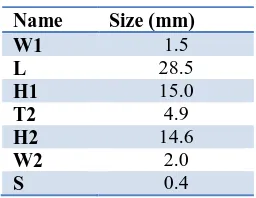
Table I show the antenna dimensions, and Table II are detailed all components used for the project, including its physical dimensions. The abbreviations Ci, with i = 1,2,3 ... 9, refers to capacitors, Li, with i = 1,2,3 are chip inductors, resistors R1 and R2 are chips U1 is the integrated circuit, and X1 is a piezoelectric crystal. The size 0402 is a code commonly used for chips, the dimensions of which are set out in Figure 1 (a) and QNF20 4X4 size is a package type whose dimensions appear in Figure 1 (b).
TABLE I. Antenna Dimensions.
Name Size (mm)
W1 1.5
L 28.5
H1 15.0
T2 4.9
H2 14.6
W2 2.0
Development and assembly of Radio Frequency Module using components with SMD technology for educational purposes
Lat. Am. J. Phys. Educ. Vol. 11, No. 1, March 2017 1304-3 http://www.lajpe.org
TABLE II. List of components.
Component Name Size Description
22pF C1 0402 NPO, +/- 2%
22pF C2 0402 NPO, +/- 2%
2.2nF C3 0402 X7R, +/- 10%
4.7pF C4 0402 NPO, +/- 0.25pF
1.5pF C5 0402 NPO, +/- 0.1pF
1pF C6 0402 NPO, +/- 0.1pF
33nF C7 0402 X7R, +/- 10%
1nF C8 0402 X7R, +/- 10%
10nF C9 0402 X7R, +/- 10%
8.2nH L1 0402 Chip indutor +/-5%
2.7nH L2 0402 Chip indutor +/-5%
3.9nH L3 0402 Chip indutor +/-5%
1MΩ R1 0402 +/-10% 22MΩ R2 0402 +/- 1%
nRF24L01 U1 QFN20
4X4
16MHz X1 +/-60ppm,
CL=12pF
It is important to note that to build this RF module, all steps have been fulfilled: Design, simulation, assembly and operation tests in three practical applications.
A. ANTENNA
The inverted V antenna was chosen because it is widely used in wireless devices. The HFSS software was used to perform the antenna design. With an iterative analysis was possible to find the best dimensions and geometries in order to improve its operation. The radiation pattern in the 2.4 GHz operating frequency can be seen in Figure 4 in 3D and 2D in Figure 5, it is possible to observe good radiation coverage.
FIGURE 4. Three-dimensional radiation pattern of the antenna
printed on 2.4 GHz.
FIGURE 5. Simulation of the electric field at 2.4 GHz.
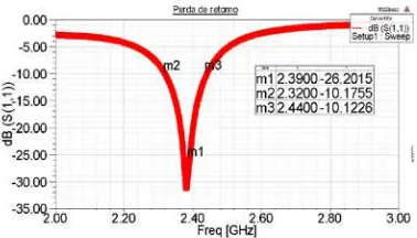
One important aspect to be considered on the integration of the antenna with the card is the impedance matching between the IC and the antenna input. The project is designed in such a way that the antenna has at its entrance, an impedance of 50 Ω. To evaluate the matching impedance of the antenna with the rest of the circuit we used the S11 parameter that represents the return loss in the antenna input. For practical purposes it is considered that a value of less than -10dB for S11 parameter ensures proper matching to the input impedance , this means a level of reflection at the entrance smaller antenna than 10 times the level of incident signal. Taking into account these criteria, in Figure 6 it can be seen the excellent matching of the antenna in the project's frequency 2.4 GHz.
FIGURE 6. Return Loss graph in dB and Frequency in GHz.
IV. ASSEMBLY
Rodrigo Luiz Ximenes et al.
Lat. Am. J. Phys. Educ. Vol.11, No. 1, March 2017 1304-4 http://www.lajpe.org
A. MATERIALS
For the construction of the module with SMD technology, the following tools were used: tweezers, solder paste 63% tin and 37% lead, bracelet / anti-static mat, bench microscope, drill 0.6mm and varnish.
B. TECHNICAL ASSEMBLY
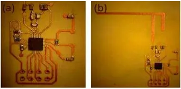
The tracks of connections shown in Figure 3 were printed on the PCB (Printed Circuit Board) using thermal transfer technique and chemical corrosion of copper [4]. A PCB with dielectric constant, εr = 2.2, loss tangent in the amount of 0.0009, copper thickness of 1/2 oz, height of substrate, H = 30 mil, was used. With the board already created, it started the manual assembly process of the components, using solder paste, tweezers and other tools. The Figure 7 (a) the material for the plate assembly are shown. In Figure 7 (b), there is highlighted in red, one SMD component superimposed above the plate even without soldering. Similarly, in Figure 7 (c) the other components were placed in positions where they should be soldered, as shown in Figure 8 (a). Importantly, prior to placement of the components was deposited solder paste to secure them in their respective above board positions.
FIGURE 7. (a) Materials used, (b) with the first overlapping plate
component even without soldering above the PCB (c)component zoom.
After this process, the plate is brought to a low cost reflow oven, specially designed and constructed in this design to accomplish the welding of SMD components on the board. For the heating furnace developed can choose one of two possible different temperature patterns, as suggested in [5]. Using this technique by reflow soldering furnace, all parts are welded at once. This technique takes advantage of the welding technique with hot air station also used for mounting SMD components, in which components are welded one at a time. For this reason, the hot-air technique is used for maintenance, i.e. in cases where they need to weld component isolated over an existing plate. The RF module already completed all welded components and including the built-in antenna is shown in Figure 8 (b).
FIGURE 8. (a) RF module with the components fixed only with
solder paste (b) RF module to the built-in antenna and welded components.
C. TECHNICAL WELDING
Figure 9 shows the block diagram oven for soldering the SMD electronic components developed in the laboratory.
FIGURE 9. Diagram welding oven block.
In the oven are used two halogen lamps for heating, installed in a metal box. The temperature is checked by a K-type thermocouple, and converted through an AD595 circuit [5] which is connected to the microcontroller PIC18F4550 [6] by analog reading pin. The microcontroller is responsible for processing information received from the sensor (thermocouple) and control the PWM (Pulse Width Modulation). The power system consists of the transistor BTA16 [7] and the integrated circuit MOC3011 [8], which was directly linked to the oven lights. A user interface was designed to display on a display welding process from the preheating furnace to the completed weld. The buttons allow you to choose the pattern of temperature with the oven will operate.
Development and assembly of Radio Frequency Module using components with SMD technology for educational purposes
Lat. Am. J. Phys. Educ. Vol. 11, No. 1, March 2017 1304-5 http://www.lajpe.org seconds one obtains the highest heating furnace. From that
moment halogen lamps are switched off and the oven begins to cool slowly without accompanying theoretical curve of cooling. It is important to note that even if the actual curve does not follow the theoretical curve of cooling, the furnace is developed within the range specified in [9] establishing a cooling rate of at most 6 °C/s. A faster cooling can lead to cracking of the welds.
FIGURE 10. Welding curve based on standards.
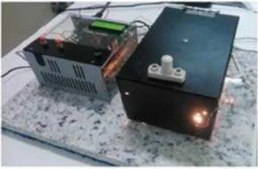
Figure 11 shows the furnace built in operation.
FIGURE 11. Oven operation.
Visual inspection of welds performed on the card in question was satisfactory, and the integrity of the components was verified with functional tests.
V. RESULTS
In order to validate the mounting, soldering and operation of the RF module made and still show its capability in achieving learning experiments were implemented three different applications. Three types of microcontrollers are the key components that make this distinction between applications. Importantly, the projected module is intended to be a management device and it has no additional feature. Therefore, it is evident the need to use the microcontroller receiving the sensor readings and send via SPI (to set up as
a receiver or transmitter) of the nRF24L01 integrated circuit component. The microcontroller has the function to access the modes of operation, it has the characteristic FIFO (First In First Out) and may access the register maps by 1 byte commands.
For this function and tests, the different microcontrollers used were: PIC16F628A [10] Arduino Uno [11] and a board FRDMKL25Z Freedom [12].
A. TEST 1 - PIC16F628A
Using the RF module developed with a microcontroller coupled to indoor object monitoring applications, connected to the project on a scheduled PIC16F628A to send an object identification code every 15 seconds. In Figure 12 there is the block diagram of the operation of the experiment.
FIGURE 12. Block diagram of operation to monitor indoor
objects.
The PIC16F628A not have the peripheral (physical layer) SPI. However, in the software by means of a simple configuration, the SPI protocol is emulated using functions in the firmware.
The microcontroller is connected to the transmitter / receiver module, as shown in Table III.
TABLE III. List of pin connections PIC16F628.
Pin Name Funtion PIC
1 GND Terra GND
2 VCC Power Supply 3.3V
3 CE Chip Enable RX/TX Pin 1
4 CSN SPI Chip Clock Pin 17
5 SCK SPI Clock Pin 18
6 MOSI SPI Slave Data Input Pin 2
7 MISO SPI Slave Data Output Pin 15
8 IRQ Interruption Pin 16
Rodrigo Luiz Ximenes et al.
Lat. Am. J. Phys. Educ. Vol.11, No. 1, March 2017 1304-6 http://www.lajpe.org
FIGURE 13. Graphic monitoring of two objects in indoor room.
A. TEST 2 - Arduino UNO
The main idea is to test two monitoring the temperature of a site as a supervisory system. For real-time monitoring temperature used the LM35 sensor with a UNO Arduino the transmitter / receiver. The module connections are shown in Table IV.
Table IV. Pin connections list Arduino UNO.
Pin Name Funçtion Arduino
1 GND Terra GND
2 VCC Power Supply 3.3V
3 CE Chip Enable RX/TX Pin 9
4 CSN SPI Chip Clock Pin 10
5 SCK SPI Clock Pin 13
6 MOSI SPI Slave Data Input Pin 11
7 MISO SPI Slave Data Output Pin 12
8 IRQ Interruption -NC-
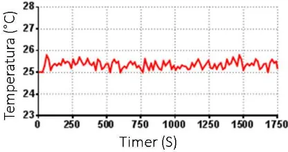
The LM35 sensor sending information over the analog input of the Arduino, which in turn treats this information, converts the voltage sensor to degrees celsius, stores the maximum and minimum values, and sends this information by SPI through the RF module. The receiving module receives the information and stores on a database. In Figure 14 there is the diagram of complete design. In Figure 15 the graph monitoring real time temperature is shown.
FIGURE 14. Diagram of the functioning blocks to monitor
temperature.
FIGURE 15. Temperature monitoring chart in an air-conditioned
environment.
A. TEST 3 - Freedom KL25Z
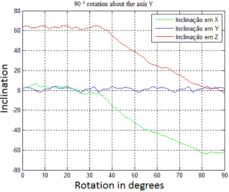
Another application was held the real-time monitoring of the accelerometer. Connected to a development board Freedom board, which already has the accelerometer sensor coupled MMA8451Q [13].
The accelerometer has the function of recognizing the projection gravity vector in each axis (x, y, z).
In Figure 16 there is the circuit block diagram mounted surrounding the transmitter and receiver modules.
In experiment was monitored in a short period of time at 90° rotation around some axis. Figures 17 and 18 show the rotations of 90 ° about the X axis and around the Y axis, respectively.
FIGURE 16. Block diagram of operation to monitoring
accelerometer.
VI. CONCLUSION
Development and assembly of Radio Frequency Module using components with SMD technology for educational purposes
Lat. Am. J. Phys. Educ. Vol. 11, No. 1, March 2017 1304-7 http://www.lajpe.org
FIGURE 17. 90 ° rotation about the axis X.
FIGURE 18. 90 ° rotation about axis Y.
REFERENCES
[1] Fratassi, S. R., Reparos em placas com Componentes SMD (Antenna Edições Técnicas, São Paulo, 2007). [2] Panasonic, Thick Film Chip Resistors, <
http://industrial.panasonic.com/www-data/pdf/AOA0000/AOA0000CE1.pdf>, visited on August 5, 2015.
[3] Sparkfun, Single Chip 2.4GHz Transceiver nRF24L01 <https://www.sparkfun.com/datasheets/Components/SMD/ nRF24L01Pluss_Preliminary_Product_Specification_v1_0. pdf>, visited on August 5, 2015.
[4] Fazendo suas placas de circuito impresso Tecnica de corosão,
<http://www.ppgel.ufsj.edu.br/uaisoccer/downloads/127206 1971.pdf>, visited on August 5, 2015.
[5] Analog Devices. Monolitic Thermocouple Amplifers with Cold Junction Compensation, AD594/AD59, <
http://html.alldatasheet.com/html-pdf/48077/AD/AD595/19/1/AD595.html>, visited on August 5, 2015.
[6] Microchip. High-Performance, Enhanced Flash, USB Microcontrollers with nanoWatt Technology-18f4550, <http://ww1.microchip.com/downloads/en/DeviceDoc/3963 2e.pd>, visited on August 5, 2015.
[7] On Semiconductor. Triacs Silicon Bidirectional Thyristors -BTA16-600BW3G,
< http://www.onsemi.com/pub_link/Collateral/BTA16-600BW3-D.PDF>, visited on August 5, 2015. [8] Texas Instruments. OPTOCOUPLERS / OPTOISOLATORS – MOC3011,
<http://www.ti.com/lit/ds/symlink/moc3011.pdf>, visited on August 5, 2015.
[9] Joint Industry Standard (USA). Norma IPC/JEDEC J-STD-020D. 1 de agosto de 2007 com revisão março 2008, (JEDEC, Arlington VA, 2008).
[10] Microchip.Flash-Based, 8-Bit CMOS Microcontrollers with nanoWatt Technology-16f628a. Available in: <http://ww1.microchip.com/downloads/en/DeviceDoc/4004 4F.pdf>, visited on August 5, 2015.
[11] Atmel. Flash-Based, 8-Bit CMOS Microcontrollers with nanoWatt Technology-arduino UNO, <http://www.atmel.com/Images/doc8161.pdf>, visited on August 5, 2015.
[12] Microchip. 48 MHz Cortex-M0+ Based Microcontroller with USB-Freedom kl25Z. Available in: <http://ww1.microchip.com/downloads/en/DeviceDoc/4004 4F.pdf>, visited on August 5, 2015.
[13] Freescale Semiconductor MMA8451Q, 3-Axis, 14-bit/8-bit Digital Accelerometer,