Layer 2 And Layer 3 Usage
Choosing Between Single And Dual Stripline Useful RF And Mixed Technology Stackups 4 Layer RF Only Design Stackup
6 Layer RF Only Design Stackup
8 Layer XYZ Mixed RF - Digital Design Stackup – Low Density Digital
10 Layer Mixed RF - Digital Design Stackup – Low To Medium Density Digital 12 Layer Mixed RF - Digital Design Stackup – Medium To High Density Digital 14 Layer Mixed RF - Digital Design Stackup – High Density Digital
Coplanar Waveguide (CPW)
Flooding Unused Areas With Ground Adding Ground Vias
Ground Shielding Vias Ground Stitching Vias Ground Transition Vias EMI Shielding Vias Shielding
Table of Figures
Figure 1. Cross Section Of Current Flow At low And High Frequencies Showing Skin Effect. Figure 2. Voltage Reflection Where Load Impedance Is Higher Than Line Impedance.
Figure 3. Voltage Reflection Where Load Impedance Is Lower Than Line Impedance. Figure 4. Power Implemented As A Wide Trace.
Figure 5. Power Implemented As A Local Plane - Potential Patch Antenna.
Figure 6. Example Of When An Impedance Mismatch Becomes An Issue - @ f = 5GHz Figure 7. Floorplan View Of X/Y Axis RF And Digital Zone Isolation.
Figure 8. Cross Section View X/Y Axis Only RF And Digital Zone Isolation. Figure 9. Z Axis Isolation Of RF And Digital Circuitry.
Figure 10. Floorplan View X/Y And Z Axis RF And Digital Zone Isolation. Figure 11. Cross Section View X/Y And Z Axis RF And Digital Zone Isolation.
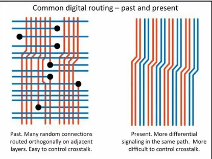
Figure 12. Layer 3 As Reference Ground For Microstrip Allows Wider Transmission Line. Figure 13. Difference Between Past And Present Typical Digital Routing.
Figure 14. Typical 4 Layer RF Only Stackup Cross Section. Figure 15. Typical 6 Layer RF Only Stackup Cross Section.
Figure 16. Typical 8 Layer Mixed RF/Digital Stackup Cross Section. Figure 17. Typical 10 Layer Mixed RF/Digital Stackup Cross Section. Figure 18. Typical 12 Layer Mixed RF/Digital Stackup Cross Section. Figure 19. Typical 14 Layer Mixed RF/Digital Stackup Cross Section. Figure 20. Typical 16 Layer Mixed RF/Digital Stackup Cross Section. Figure 21. Differences In Fiber Density With Different Weave Styles. Figure 22. Advantages And Examples Of Via In Pad Technology.
Figure 23. Resistive Model Of A DC Or Low Speed Transmission Line.
Figure 24. Complete Model Of A High Speed Transmission Line Showing Parasitic Elements. Figure 25. Microstrip Transmission Line Construction.
Figure 28. Coplanar Waveguide Transmission Line Construction.
Figure 29. Example Of Keeping Input And Output Of A Circuit Block Well Distanced. Figure 30. Amplifier And Filter With Overlapping Loop Areas.
Figure 31. Modified Amplifier Bypassing To Reduce Loop Area.
Figure 32. Floorplan Of Typical RF Modem Design With Baseband Processing And Power Supplies.
Figure 33. Noise Transients Can Travel Anywhere On The Board.
Figure 34. Well Selected And Placed Decoupling Capacitors Can Keep Power Planes Much Cleaner.
Figure 35. Bypass Capacitors On Analog Device Can Remove Noise Already Existing On Power Connections.
Figure 36. Bypass Network Frequency Response With All Low ESR Capacitors.
Figure 37. Bypass Network Frequency Response May Improve If One Or More Capacitors Have Higher ESR.
Figure 38. General Placement Of Discrete Parts Around Large Integrated Devices. Figure 39. Placement And Via Usage For BGA Bypassing.
Figure 40. Placement And Connections For Bypassing QFP With Thermal Pad. Figure 41. Placement And Connections For Bypassing QFP Without Thermal Pad.
Figure 42. Connections To Power Plane For Decoupling Capacitors Around High Density Digital Devices.
Figure 43. Connections To Plane With Bypass Capacitors ‘On The Way’ For An Analog Amplifier. Figure 44. Slot In Ground Plane Causes Long Ground Return Path.
Figure 45. Example Placement With Resulting Return Paths And Loop Areas. Figure 46. Adding A Ground Plane Split To Restrict Ground Current Paths.
Figure 47. Stub Caused By A Through Via Being Accessed On An Internal Layer.
Figure 48. Back-drill Eliminates Most Of The Stub, Blind Via Or Microvia Eliminates The Stub. Figure 49. Routing The Same Connection With And Without Stubs.
Figure 50. Improved Placement And Via-In-Pad Technology Can Easily Remove Stubs In RF Design. Figure 51. Offset Pad Origin Can Resolve DRC Errors On Small Components.
Figure 52. Footprint Based Rule Area Can Resolve DRC Errors On Small Components.
Figure 54. The 90 Degree Corner - Worst Case Method And Best Case Method.
Figure 55. Different Ways To Implement 90 Degree Bends in RF Transmission Lines. Figure 56. Impedance Mismatch Area With Simple T-Junction.
Figure 57. T-Junction Impedance Mismatch And Commonly Used Compensations. Figure 58. Transmission Line Geometry Does Not Match Component Pad Geometry. Figure 59. Removing Planes Copper Beneath Large Component Pads.
Figure 60. Stepped And Tapered Matching Of Transmission Line To Pad Geometry. Figure 61. Ground Stitching Along RF Signal Paths - Maintain 3H Spacing To Traces. Figure 62. Ground Stitching Along RF Traces And Under Perimeter Shield Walls. Figure 63. Ground Stitching Vias Added Where Space Permits Around The Design. Figure 64. Effect On Ground Return Current If There Are No Ground Vias Nearby Figure 65. Ground Vias And Antipad At Differential Pair Layer Transition.
Figure 66. Some Typical Perimeter EMI Shielding Via Patterns.
Figure 67. An Example Of Standard Off The Shelf Shielding Products.
List Of Tables
Table 1. Common Circuit Board Materials Of Different Compositions With Loss And Dielectric Constant.
Table 2. Suggested Layer Usage For Typical 4 Layer RF Only Stackup. Table 3. Suggested Layer Usage For Typical 6 Layer RF Only Stackup.
Table 4. Suggested Layer Usage For Typical 8 Layer Mixed Technology Stackup. Table 5. Suggested Layer Usage For Typical 10 Layer Mixed Technology Stackup. Table 6. Suggested Layer Usage For Typical 12 Layer Mixed Technology Stackup. Table 7. Suggested Layer Usage For Typical 14 Layer Mixed Technology Stackup. Table 8. Suggested Layer Usage For Typical 16 Layer Mixed Technology Stackup.
Acknowledgements
The author would like to express thanks and appreciation to the following people, without whom it would not have been possible to put this guideline together.
Nick Barbin. President - Optimum Design Associates. For providing the idea, encouragement, patience, and the time to compile and present the guideline. This guideline took many hours to produce and would not have been possible if the time was not proved to do so.
Scott Nance. Senior Designer - Optimum Design Associates. For his invaluable assistance in so many ways. Scott spent many hours reading word by word, providing extremely useful content, corrections, feedback and suggestions for improvement. Scott has also presented this guideline in slide
show/discussion form at trade shows and at specific customer sites.
Rick Hartley. Industry recognized consultant on the topic of High Speed and Mixed Technology Design. Rick was kind enough to volunteer his time to read the guideline completely and provided much extremely useful feedback and some very critical and needed corrections to the content.
Robert Frank. Marketing Manager - Optimum Design Associates. For many hours of proof-reading, grammar correction and for getting this book published.
Forward
This guideline is presented as a practical guide to the physical layout design of RF and, in particular, mixed technology circuit boards. Mixed technology refers to the combination of low frequency
analog, high frequency RF, power supplies, digital circuitry and even motor drivers, all in a single design. The guideline does not present pages of RF theory and formulae, those are for the electrical engineer and the engineering design has already been done by the time the circuit board layout process is started. Some formulae and theory are presented however, not for the day to day design process but more as an aid to understanding some of the things layout designers need to consider more for mixed technology design than would be the case in a purely digital design. One of the main aims of this guideline is to use plain words wherever possible to present information that is normally presented with a lot of formulae, numbers and theory and which is, quite frankly, lost on most layout designers. What the layout designer needs is information on what to do at the circuit board level when designing the physical layout, not the engineering circuit. The circuit board layout process is the last real design phase in the product development cycle, and it is certainly the phase that is normally placed under the most pressure in terms of time to complete, because everything that comes before it always takes longer than the time budgeted. As a result, the layout designer needs to be as efficient as possible and make use of proven methods and techniques to complete the task in as timely a manner as possible while still being technically correct. The issues faced when designing circuit boards for RF and mixed technology applications that are not usually considered so critically in designs for only digital applications will be described. Techniques and methods will be presented that have been used consistently over many years of designing circuit boards for all types of applications, many of which were for radar systems, RF modems and satellite payload systems.
Some of these methods and techniques may be considered technically unnecessary or may well conflict with what some designers currently do or are advised to do by their peers, but everything presented in this guideline has been used very successfully over a long period of time designing mixed technology circuit boards. There is no ‘one size fits all’ solution to the challenge of mixed technology design. There are many different views and approaches to the problem. Electrical
engineers, layout designers, actual designs, constraints and CAD tools each differ greatly and yet we are still able to produce designs that work well despite all these variations, so there are clearly many methods that do work well. Although this guideline is much more for layout designers rather than the electrical engineers, there is also much useful information for electrical engineers which will help them to understand some of the real world design, fabrication and assembly issues that layout
So What’s The Difference Between Analog And
Digital?
Understanding the main differences between these two design types is a key part of understanding why some things the layout designer does will have a more significant effect in one design type versus the other. In truth, the more challenging design is still the analog one, because the big difference is that in analog design some things need to be considered a lot more carefully than they would be when doing a purely digital design. A layout designer still needs to consider the same things in digital design, but often to a significantly lesser degree because digital designs can be reasonably tolerant to many of these issues. Having said that, as operating frequencies increase and logic voltage levels decrease in digital circuits, layout designers are finding that issues traditionally more important in analog circuits are becoming just as important in digital circuit layouts. The differences between digital and analog domains are, with respect to circuit board layout, becoming less and less obvious.
Information Integrity.
Just as in a digital design, the critical issue in an analog design can be thought of as being ‘information integrity’. In a digital design the information is being conveyed by means of ‘ones and zeros’, the circuits generate and respond to discrete voltage levels representing a binary 1 or 0. Typically a high voltage represents a 1, and a low or zero voltage represents a 0. There is usually no information conveyed by voltage levels other than those. In an analog design, information is conveyed, in different ways, by voltage levels continuously variable from microvolts to tens or even hundreds of volts. Similarly, the frequency in a digital system, with few exceptions, simply controls how fast the data is conveyed or processed, while in an analog system the frequency of a signal often IS the information content of the signal. The phase of an analog signal and its relationship to the phase of another signal is often the information content of an analog system as well.
Amplitude, frequency and phase are also extremely important in a digital design, but digital systems are usually more tolerant to some degradation in all of these, some to a lesser extent than others. However, in an analog system, there can be very little tolerance to degradation in any of these parameters because they ARE the information being processed.
Do We Still Use Analog?
While we may be living in the digital age, analog circuits are still prevalent, and we use them every day. Equipment with significant analog circuit content includes things like cell phones, audio
amplifiers, instrumentation amplifiers, radio receivers, data acquisition and measurement circuits, medical imaging, monitoring and treatment equipment, power supplies and, of course, RF and microwave circuits used in satellite and radar systems. Most equipment using analog circuits today also includes some digital circuitry. For example, an audio amplifier/receiver contains a lot of
What’s The Frequency?
With analog and RF systems, signals tend to consist of a single or small number of fundamental frequencies. There are usually multiple signals of interest, but it is a smaller number of different frequencies or a specific range of frequencies that the layout designer is concerned with. All other frequencies present would be considered as noise or interference signals which need to be controlled or filtered out so that only the frequencies of interest are processed as effectively as possible. There will, of course, be some harmonics of these intended frequencies present but typical RF designs utilize many filters in the signal path to ensure that only signals of the frequencies of interest are passed to or from circuit blocks. In digital designs, signals are what we call square waves. A square wave is actually the sum of a sine wave of the same (fundamental) frequency, plus all the odd
When Does Analog Become RF?
Traditionally, analog circuits were low frequency systems for supply of power and for voice and audio signal processing, because that’s what we developed electronics for first – the telephone for example. RF circuits were developed for long distance real time communication, where we could now transmit our voices over long distance through Radio Frequency waves rather than having to have a solid wire between two or more points. These systems produced, transmitted and received radio frequency signals ranging from hundreds of KHz to hundreds of MHz.
It has become normal to think of RF as being in the 3 MHz – 300 MHz range. Analog circuits operating in the 300 MHz – 300 GHz range were traditionally referred to as microwave circuits. There are many opinions on when an RF signal becomes microwave, with above 300 MHz is the generally accepted point. Between 30 GHz and 300 GHz is often referred to as Millimeter Wave because the wavelength in this band ranges from 10mm to 1mm, but generally microwave refers to everything above 300 MHz.
Converging Domains
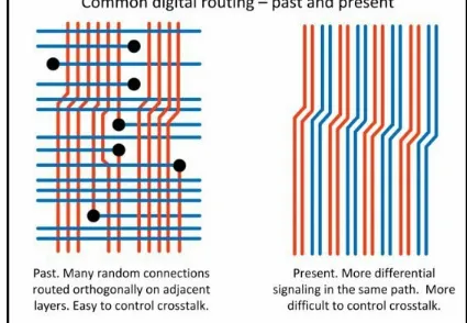
Much of what is presented in this guideline will use terms most layout designers have already heard in reference to digital designs. Impedance matching, transmission lines, return loss, coupling, noise and interference, crosstalk, delay tuning, signal integrity etc. are all terms layout designers have become familiar with over the last decades. That is because these are predominantly high frequency related terms describing phenomena that layout designers need to be aware of, and are becoming more prevalent because digital designs are operating at higher and higher frequencies all the time. Well, it is not new terminology by any means. These are things that have been the concern of RF and analog electrical engineers and layout designers for the last 50 years or more. In the early days of digital systems, voltage levels were 5 Volts, 10 Volts or even higher. Frequencies were in the hundreds of KHz and very low MHz ranges with much longer rise times than is the case today. At these low frequencies, and with these voltage levels (the voltage levels required to cause a change from a 0 to a 1 were in the order of 3 volts or more) there was an inherent immunity to noise virtually built in. There was much less noise to consider anyway, because such slow circuits did not cause much significant radiation. Today, some digital circuits are operating at sub 1 Volt levels, with the logic thresholds diving into the hundreds of millivolts range, and with frequencies into the GHz ranges with sub-nanosecond edge rates, so the high frequency content and EMI radiation are much increased. Today’s high speed digital designs really do need to be treated as low level high
Loss
One of the primary concerns in analog and RF systems is the efficient transfer of power. All of the signal power present at the output of any circuit block should ideally be transferred to the next stage of the circuit. When a signal needs to be attenuated, it should be done in a controlled manner using an attenuator device that will produce predictable and repeatable results. Signal power losses due to non-circuit elements like impedance mismatch, incorrect transmission line design or material selection issues are potentially detrimental to the functioning of the circuit. Some losses are
Dielectric Loss
Dielectric loss, specified as dissipation factor (Df) on a vendor’s datasheet, (which will never be zero), is inherent in the laminate and prepreg materials used to fabricate the board. It is the loss of energy that goes to heating a dielectric material in a changing electromagnetic field and, in circuit board laminates, is a function of the materials’ molecular structure and resin type and content. There are a very wide range of materials available, some of which exhibit dielectric loss orders of
magnitude lower than others. Dielectric loss is proportional to frequency, and is therefore more critical to consider with higher frequency lower power designs.
Material Composition Df@10GHz Dk@10GHz Tg Relative PCBcost/Mfg Tier ISOLA
370HR Epoxy/Woven Glass 0.025 3.92 180 1-FR-4
ISOLA
FR408HR Epoxy/Woven Glass 0.0095 3.65 190 2-LowLoss
NELCO
N4000-13 EP
SI Epoxy/Cyanate Ester/WovenGlass 0.007 3.2 210 2-LowLoss PANASONIC
MEGTRON 6 Epoxy/PPE/Woven Glass 0.004 3.3 185 3-UltraLowLoss ROGERS
RO4350B Hydrocarbon/Ceramic/WovenGlass 0.0037 3.48 280 3-UltraLowLoss NELCO
7000-2 V0 Polyimide/Woven Glass 0.010 3.8 250 4-Performance ARLON
CLTE XT PTFE/Ceramic/Woven Glass 0.0012 2.94 230 4-Performance TACONIC
TacLamplus PTFE/Metal Backed 0.0004 2.1 230 5-Custom
Formulae and equations can be found that will translate this information into dB loss values at particular frequencies. That level of detail is not presented here because, as a layout designer, the main concern is, “What am I contributing to loss?” Dielectric loss is beyond the control of a layout designer unless the layout designer is also entirely responsible for material selection. Lower loss materials are more expensive, so, in many cases, they are not even a consideration. The layout designer needs to be aware of the phenomena and which materials are better for a particular design, in order to make valid recommendations regarding material selection.
In an analog design, when a signal is injected into a transmission line, the frequency of the propagated wave will be unchanged, but the amplitude will be decreased due to dielectric loss. The amount of loss will be dependent on the length of the transmission line, and the frequency of the signal (because dielectric loss is proportional to frequency). This is one of the reasons we always strive to keep higher frequency connections as short as possible. Extremely low level analog circuits, such as instrumentation amplifiers or low power receiver front ends, require consideration of dielectric loss because of the intolerance of these circuits to amplitude loss.
Digital signals are square waves, which consist of the fundamental frequency plus an infinite number of embedded sine waves at odd harmonics (odd multiples of the fundamental frequency) and at
diminishing amplitudes. Digital signals generally have very strong amplitude at the fundamental and lower harmonic frequencies up to an approximate frequency as determined by the equation:
f = 0.35 / T
rwhere f = frequency in GHz and Tr = Signal Rise Time in nanoseconds.
Skin Effect
Conductor loss is related to the way current flows in a conductor. At low frequencies, current in a conductor will flow in the entire cross section of the conductor. At higher frequencies, current tends to concentrate in the thin outer portion of the trace. (See Figure 1) This is known as Skin Effect. This phenomena effectively reduces the cross sectional area of the conduction path, making it more
resistive. This can be offset to a certain extent by using wider traces where impedance modelling allows. Wider traces will exhibit less variation in resistance with frequency so the trace will be less lossy. Because it increases the effective resistance of the signal path, skin effect also has an effect on transmission line impedance, making selection of the correct termination resistor values more
complex.
Smooth surface is better.
Copper surface roughness contributes to increased loss due to skin effect because the overall resistance of the path is a function of the path length. At higher frequencies, the skin effect causes the current to flow in a much thinner region of the trace, at or near the surface. The rougher the surface is, the longer and therefore more resistive will be the signal path.
The approximate skin depth of copper is:
Skin Depth (cm) =
or Skin Depth (inch) =
It is also known that there will be considerably more current flow in the surface closest to the
Return Loss Or VSWR
A full discussion of return loss and Voltage Standing Wave Ratio (VSWR) would easily be the subject of an entire book by itself. A detailed examination would involve a large amount of very complex mathematics to explain what becomes quite a dynamic issue, when changing signal
frequencies and amplitudes, along with transmission line characteristics, variable source and load impedances and skin effect are all combined. Such a discussion is beyond the scope of this guideline, and is actually more in the engineering domain than in the circuit board design domain. Usually the most significant contributor to loss in an RF design is return loss. This is the loss caused by mismatch between the output impedance of a driving source, the characteristic impedance of the connecting transmission line, and the input impedance of the receiving load. This discussion assumes a voltage source with a purely resistive output impedance providing a single frequency sine wave into a purely resistive line and load. There are a limited number of things that a layout designer can do to either cause or help resolve return loss and VSWR issues.
Impedance is a frequency dependent quantity. This means the characteristic impedance of the
transmission line and the source and load impedances will vary with frequency. When a signal travels along a transmission line and then arrives at the load, if there is a mismatch between the characteristic impedance of the transmission line and the impedance of the load, then a portion of the signal will be reflected back along the transmission line towards the source. The polarity and magnitude of the reflected signal depends on whether the load impedance is higher or lower than the line impedance: (assume that the source and line impedances are perfectly matched.)
If the load impedance exactly matches the line impedance then there is maximum power transfer to the load and there is zero reflection. (Ideal situation that virtually never happens).
If the load is an open circuit, there will be a voltage reflection of equal amplitude from the open circuit end of the line reflected back towards the source, and this voltage will be in phase with the incident wave. This reflected voltage will add to the incident wave originally propagated on the line, effectively doubling the voltage on the line. When the reflected voltage reaches the source it will be absorbed by the source impedance and the whole line will settle at the source voltage.
If the load is a short circuit there will be a voltage reflection of equal amplitude from the short circuit end of the line reflected back towards the source, and this voltage will be opposite phase to the
incident wave. This reflected voltage will subtract from the incident wave originally propagated on the line and, when the reflected wave reaches the source, the voltage at the output of the source will be zero (and the source generator device will likely be broken!).
Figure 2. Voltage Reflection Where Load Impedance Is Higher Than Line Impedance.
Figure 3. Voltage Reflection Where Load Impedance Is Lower Than Line Impedance.
The amplitude of the reflected wave relative to the incident wave is known as the Reflection Coefficient. ( )
And is calculated as:
Where = reflected voltage and = incident voltage
This is equivalent to
Where = load impedance and = transmission line characteristic impedance.
Now, assume a transmission line with non-matched load impedance is being driven with a continuous single frequency sine wave and the line is of such length that the signal takes many full cycles to reach the end of the line:
Since any transmission line has an associated propagation delay, the phase of the reflected wave with respect to the incident wave is continually changing. The total amount of initial phase change relative to the incident wave will be dependent on the length of the transmission line and the frequency of the wave. Because of this, there will be some points along the line where the incident wave and the
wave will subtract from the incident wave. The points where the incident and reflected waves are in phase and opposite phase are the points where maximum and minimum amplitude will appear on the line. The maximum and minimum amplitude points will alternate along the line. If the frequency stays constant, then this condition will become stable and the combined wave, the incident wave plus the reflected wave, will appear to be stationary on the line. This is known as a Standing Wave.
Of course, in the real world the frequency and amplitude of the incident wave and the reflected wave is continuously changing, as is the phase relationship between them. The resulting incident plus/minus reflected wave at any given point along the line is still known as the standing wave. The relationship between the standing wave and the incident wave is known as the Standing Wave Ratio (SWR), or commonly the Voltage Standing Wave Ratio (VSWR), given as:
Where = reflection coefficient.
If the source impedance and the line impedance are not matched, then the reflected wave will not be completely absorbed by the source impedance and there will be another reflection generated in the forward direction from the source towards the load. This is essentially what causes ringing.
There are two issues of major significance caused by high return loss.
The reflections, and likely ringing, add noise to the system. This degrades the quality of the original signals and can make it harder for the receiving device to distinguish the intended signal from the noise. This can significantly reduce system performance while at the same time increasing system EMI issues.
Reflected power does not get absorbed in the load. This loss in power reduces system efficiency and performance. If the load is an antenna then the output power delivered to the antenna will be less than intended
Where does the lost energy go.
Noise / Coupling / EMI / Shielding
Analog and RF circuitry is particularly sensitive to noise and this needs to be managed by controlling coupling and EMI as much as possible. Within the RF circuit, keeping the physical loop areas of both signal and power circuitry as small as possible will certainly help with this. Large loop areas are antennae and will radiate much more than small loop area circuits. This is usually fairly easy to control with a number of methods: giving more attention to component orientation and placement in the signal path, carefully and deliberately dividing the analog circuit into separate functional blocks, keeping power supply bypassing as close as possible to the device, and using wider, lower
inductance traces for power connections. One of the most effective ways to reduce EMI and EMC issues is by adding shields around sensitive circuits to help keep noise out, or around noisy circuits to help contain radiated noise emissions.
With digital designs, the faster the rise time of the digital signals, the more harmonic frequencies are present. If noise at these frequencies finds its way into analog and RF circuits on the same board, or in the same system, then the results can be disastrous for the RF circuits. Digital noise can be induced in an analog circuit either by conductive coupling or electromagnetic coupling.
Conductive coupling occurs most often by way of shared power supplies where digital noise is present on the power rail, and then that same power is used to supply an analog circuit without the necessary amount of filtering or isolation. Digital noise can also be conductively coupled by means of digital signals that are used to control some of the RF devices. These signals, often derived from FPGA and other high speed digital processing devices, will often have unnecessarily fast edge rates. Such signals, (Enable, Select, MUX Addresses, etc.) are for mode and configuration changes and are fairly static in nature, and the RF device does not normally need these to be fast edge rate signals. It is always good to isolate these with opto-electronics or buffers with the RF device side having as slow a rise time as allowed by the RF device. Another method of slowing the edge rate on otherwise static signals is to add a very high value resistor to the driver output (hundreds of Ohms up to 1k Ohm).
Electromagnetic coupling is usually in the form of radiated emissions from the high speed digital circuits which finds its way into the analog circuits by way of proximity. This is most easily controlled by maximizing the distance between the two circuit domains, and the use of grounded shielding boxes around the sensitive analog circuitry.
radiate a lot more and that can cause EMC issues.
Clean Power Delivery
Providing clean power to an RF circuit is extremely important because noise on the power supplies of an amplifier, for example, may be amplified and appear at a considerably higher level at the output. It may also cause circuits to resonate if the noise is of just the right frequency. Clean power includes clean ground, and in analog designs this is particularly important. Many analog and RF circuits are very sensitive to the absolute voltage of a signal relative to zero, and if ground is offset due to noise or excessive inductance in the ground path then circuits may behave in an incorrect manner as a result.
Most designs today will have one or more main switching regulators very near the power input connectors, and these regulators will provide the main, board-wide input voltage to other regulators and usually the global digital power supply. For example, the main input power may be 24 Volts --usually filtered right at the input connector. There may be a high current switching regulator to provide maybe 12 Volts for distribution around the board, where it is used as the input to multiple regulators providing various voltages for use at each specific circuit. Also located near the power input there will often be another high current switching regulator to provide the global digital voltage for the board, typically 3.3 Volts or 5.0 Volts. The outputs of both these, and possibly other global voltage regulators located at the power input area, need to be thoroughly filtered before these voltages are distributed around the board. There should be a range of different value capacitors at the outputs of these power supply circuits to remove any switching spikes caused by the regulators themselves. Then these clean global voltages can be safely distributed around the board to local regulators and filters.
also be the source of serious EMI issues either by themselves or when included on a circuit board with many other circuits of different technologies. Complete understanding of the circuit and the critical current paths allows layout designers to produce at least as good, usually better results, both in terms of individual circuit functionality and the entire design which may be made up of many different circuits operating together on the same board.
It is also unlikely that the manufacturer’s recommended layout will fit in a particular design exactly the same way it appears in the layout guideline, typically due to physical area constraints or different component selections, or both. This is not usually an issue as long as the key principles and written recommendations are followed. Layout designers would be better served by reading and
understanding the device functional descriptions in the manufacturer’s datasheets and then applying that knowledge, along with the understanding of where the energy in the circuit is, and referencing the sample layout in the guidelines, when implementing the printed circuit board layout. Most any circuit can be placed in a different manner and still meet all the specified guidelines.
There may very well be other high current low voltage switching regulators in the design, typically for FPGA and microprocessor core voltages of around 0.9 Volts – 1.2 Volts and maybe for DDR memory at 1.2 Volts or 1.8 Volts. It is best to locate these device specific switching regulators as close to the load circuits as reasonable, making it less likely you will be carrying switching regulator noise over larger areas of the design unnecessarily. It also makes the plane areas for these voltages smaller and therefore less resistive and less inductive. The design of split planes is also simplified, because these localized individual planes use less space, leaving more usable space for other voltage planes on the same layer(s). Care must be taken in doing this though, it is much more important to keep these switching regulators for digital circuitry physically away from analog circuits than it is to have them close to the digital circuit that uses them.
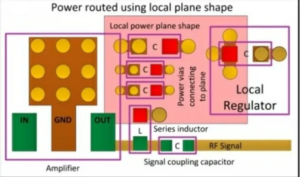
right size and shape. This small plane shape could easily resonate and cause significant EMI radiation. When there is a global or reasonably large power plane this is not an issue because the plane area is too large. Very small plane shapes used for a single device though, may be of a small enough size to be an issue. The presence of a large global ground plane on the adjacent layer can make the patch antenna issue even worse, as the size of the ground plane relative to the small power shape (patch area) will considerably alter the effective resonant frequency and gain of the patch antenna. When a local regulator is used to supply power to a single device in an RF circuit ‘room’, it is usually better to use a wide, low inductance trace to route the power rather than a very small shape on a plane layer.
This is quite different to the situation in a digital design where power/ground plane pairs with increased inter-plane capacitance, along with a good distribution of multiple values of decoupling capacitors, are required to deliver energy across the broad range of harmonic frequencies commonly found in digital circuits.
The Schematic And Mechanical Drawings
The Circuit Blocks
The next step, and a very important one, is to group all the parts based on schematic circuit blocks. This is done on all design types, but for RF designs it can be even more useful. Some of the parts in an RF circuit can be very large, devices such as filters, splitters, mixers etc. can often be inches in size. The RF part of the design is very likely going to be broken into multiple smaller circuit blocks with each one placed in an isolated room with shield walls around them, so the layout designer needs to see just what components are in each circuit block to have a good appreciation of how much space that block is going to require.
Using blocks to visualize circuit flow.
Remember, any given block will need to take input from and provide output to other associated blocks so it is important to be able to visualize this signal flow as clearly as possible before starting the component placement.
During this stage the layout designer should also be doing a mental review of the schematic. For example, one useful technique is to color unconnected pins and nets in the CAD tool white, because this makes it very obvious when some errors or omissions exist in the schematic. If there is a large white copper area under one of the RF filter parts, or the large thermal pad of a QFP device, or one of the pins of a resistor, capacitor, inductor or diode for example, then it is immediately obvious that this is a schematic omission which should reported back to the electrical engineer.
Designing The Z Axis Stackup
The next step is usually the layer stackup definition. This is also an important piece of information to have before placement starts in an RF circuit board design. Most importantly, determining the trace width to be used for the RF transmission lines and which layer in the stackup is going to be the reference plane for these RF transmission lines is needed prior to placement. It is preferable to use a wider trace for RF transmission lines for a number of reasons.
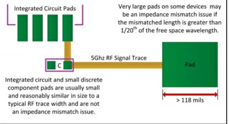
- A trace width that is as close as reasonable to the width of the majority of discrete and
integrated component pads used in the RF path is preferred, and is usually not too difficult to achieve for the majority of small chip components and integrated circuits. This helps to maintain constant impedance in the signal path. Return loss is one of the most critical issues in RF and high speed digital design, and this is affected by impedance mismatch more than anything else. If a narrow trace is used, say 6 mils wide, for the RF transmission lines, with most of the component pads being 30 mils or more in width, then there can be a significant change in impedance when the transmission line enters the pad, and this can possibly cause reflections. With that said, component pad to trace width differences are not really a serious issue in terms of impedance mismatch as long as the length of the width ‘discontinuity’ (usually the component pad) can be termed a ‘lumped distance’. That is, the length of the discontinuity is less than 1/20th of the rise time
wavelength in digital circuits or less than 1/20th of the free space wavelength of the signal
- Skin effect is another issue in RF design because of the high frequencies involved. Narrower traces exhibit higher loss due to skin effect. Narrower traces also exhibit higher resistance and inductance, both of which are undesirable attributes in an RF trace. Wider traces, however, have higher capacitance due to their larger surface area, but this would have been considered in the impedance modelling process and usually does not cause a problem. Referencing a plane further away in the Z axis is a good method of increasing the trace width for critical impedance controlled signals. Doing so, however, requires increasing the trace to trace spacing in order to keep crosstalk under control, but this is not generally an issue in RF designs because there are much fewer connections to consider than there are in a digital design.
that the best solution can be arrived at for a particular design.
Layout designers will often request material stackup and impedance model specifications from different fabrication vendors and possibly be confused with the variations found in the results, not so much in the material stackup although there will likely be some differences there, but particularly with variations in impedance models. This is certainly not unusual. Different vendors will have differences in the many processes involved in the creation of a multilayer circuit board, and each vendor is experienced with their own tolerances and processes. There are also many different software tools used for modelling the impedances, and they do not all yield exactly the same results for the same inputs. The stackup provided by the fabrication vendor can usually be accepted unless there is a large difference, more than 10 – 15%, in the impedance models from what was expected. Variations of less than 10% are to be expected and are acceptable because, after fabrication, the vendor is still responsible for certifying the characteristic impedance meets the specified values and tolerances. This acceptance allows the vendor to produce the circuit board with their processes and tools and be able to meet the specifications provided. When the material stackup and trace widths are not to deviate from what has been specifically defined by the layout designer or the electrical engineer, then notes must be added to the fabrication drawings to prevent the fabrication vendor from making changes to the tooling that would normally be made in order to meet the defined impedance specifications. Doing so, however, also means that the fabrication vendor cannot reasonably be held responsible for the measured impedances, as long as the trace widths are within tolerance, because they were prevented from doing their normal process which includes adapting the models to fit their fabrication processes and capabilities.
top side. The digital and power circuit boards were separate to this and contained only the digital or power circuits using stackups suitable for those circuits. Those were the days, simple designs with only a single technology to consider on a single board. A simple four layer design doesn’t often do it any more though, we need to put all these technologies on the same board now. We still want to have the RF circuit path on the top side, and ground on layer 2, but from there down the stackup may be very different. This is driven both by component selection in the case of BGA devices and other high density device packages, and by the amount of non-RF routing and power supply routing for the multiple different voltages needed in today’s designs.
The most common stackups used for these mixed technology designs are 8 - 16 layers. Occasionally stackups with even higher layer counts are needed, but that is driven almost entirely by the need for more route layers to escape larger BGA packages, and for additional power planes since today’s digital circuits use higher pin density components and many more different power voltages then previously. Typically though, 8 – 16 layers is enough for most mixed technology designs because the BGA devices found in these designs are not usually very large, maybe 256 – 600 pin devices and these are usually quite easily routed on 2 or 4 internal route layers.
Authors note: - Different Grounds:
Slots And Splits In Power And Ground Planes
The information presented in the following sections is about defining isolation areas and printed circuit board stackups for RF/analog and digital circuit zones on a single printed circuit board. Before that, however, it is necessary to discuss the often divisive topic of whether or not to use slots or splits in power and ground planes to isolate analog and digital return currents and noise. The discussion is primarily focused on Ground planes. This is the subject of much discussion in the industry, and will continue to be so for a long time to come. Many mixed technology printed circuit boards have been successfully designed employing solid, slotted and split ground planes without issue. The use of splits in planes, like many issues faced by layout designers, is often dictated by others and the decision about whether to use solid or split planes may not be left to the layout designer. Using and routing with solid, slotted or split planes is mentioned in multiple sections in this guideline.
High speed return current
Most layout designers involved in mixed technology printed circuit board design today will still use either slotted or split ground planes in an effort to isolate digital return currents from analog circuit areas of the board. This is mainly because it has –“always been done that way”-. There are those however, who prefer to use solid ground planes whenever possible, and believe that nothing beneficial can be gained by using slotted or split ground planes. This is based on the understanding that a high speed return current flows in the path of least impedance, not the path of least resistance, and the least impedance path is in the plane directly adjacent to the signal itself. With a solid ground plane, the high speed return current does not spread out across the plane.
Fringe fields
benefit in pulling back the power planes unless the power plane is sandwiched between two ground planes and that is not normally the case in most stackups. It is becoming more common to use a 3H rule for power plane pullback, and that is often a distance of around 10-15 mils.
A common method employed to eliminate fringe fields radiating at the edges of the board is to place a ground via fence around the perimeter of the board. These vias are placed closely together, relative to the wavelength of the highest operational frequency used in the design, and provide an extremely effective barrier to radiation. The vias are always connected either to the main board Ground or to a Chassis Ground which may in turn be connected at one or more locations through ferrite beads to the main board Ground.
That said, the fringe fields issue is not restricted to the edges of the printed circuit board. If layout designers use heavily split planes then the result is a lot more plane edges and therefore potentially more thin wire antennae distributed around the board and an increased risk of EMI.
Some exceptions
There are some situations where a split or slotted plane, or a void in a plane is required.
- At very low frequencies ( < 25 – 50kHz, there are differing opinions on where the threshold of ‘low frequency’ is. ) often in audio, motor control and switched mode power supply circuitry for example. In these designs the frequencies are so slow that the return current does often spread over the ground plane, taking the path of least resistance instead of the path of least impedance. Slots are often employed to restrict the path of return currents in these circuits.
- Safety isolation requirements where ESD or lightning suppression is needed. These designs often use splits to isolate grounds or even voids to remove all copper under certain areas of the design.
Power planes
Successfully splitting power planes is dependent on the stackup. Consider the following 10 layer stackups:
Isolate In X/Y Axis
Because we are doing mixed technology design, we will need to pay careful attention to how we will isolate these different circuit types from each other. The easiest way is to do the simple X/Y axis isolation, by defining different areas of the board for different circuit types. This works well when the density, particularly in digital circuits, is low enough and the separation between circuit types is very clearly defined. When this method of isolation is used it is common, although seen by some as unnecessary, to have a slot in the ground and power planes with a bridge area where the zones are joined and all digital control signals for the RF circuitry must be routed over this bridge. Many electrical engineers and layout designers, prefer to never use slotted or isolated ground planes though. It can be argued that, if the design is placed and routed in the proper manner, then slots in the planes have no beneficial effect. This is because the high speed signal return currents will flow in the ground plane adjacent to the signal path and will be directly under or over the signal path itself, (the path of least impedance) and will therefore not be circulating in other areas. When a board is designed without slotted or isolated planes, then the slot areas shown in Figure 7 are seen simply as ‘borders’ or ‘no go zones’ for routing. When slotted or split planes are used, all connections between the digital and RF zones must be routed over the ‘bridge’. There will be times when the electrical engineer or customer demands that the planes be slotted. This should not present a problem as split, slotted and solid planes can be used effectively so long as the solid plane methodology still essentially respects the no go zone where the slot would be. This means that different circuit areas should be visualized as being separated by slots or splits, even when a solid plane is used, and those visualized separations are seen as no go zones for routing. This methodology helps to contain digital and analog routing in their own respective zones which is more than enough to ensure proper isolation.
The following stackups and descriptions are based on the presence of slots or splits in planes to isolate analog and digital zones, since it is recognized that this is still the method used by most layout designers. The same information holds true for layout designers who do not use slots or splits in planes as long as the above visualization is employed.
Figure 8. Cross Section View X/Y Axis Only RF And Digital Zone Isolation. Notes X/Y axis isolation:
- The slot area in Figure 7 and Figure 8 does not have to be a physical slot cut out of the board, it may also be a copper layer slot, or moat, used to divide the RF and digital ground zones. The slot is generally bridged on a ground plane in a single location, and this is where the digital signals cross into the RF zone, they must be routed over the ground bridge so the return current for these signals will flow back to the digital ground zone via this ground bridge. With careful design the slot can simply be a no go zone for anything other than ground between the two circuit types and the planes can be solid.
- When X/Y only isolation is used, it is best to try to organize the placement such that any low speed digital control signals that transition between digital and RF zones actually route as little as possible into the RF zone. Try to locate components in such a way that the digital control pins are close to the bridge between the zones. This will minimize digital return currents in the RF zone. Layer 6 in Figure 8 above shows digital signal routes in the RF zone. In practice, these should penetrate the RF zone little as possible and the remainder of layer 6 should be a ground flood in the RF zone. When the ground flood is applied, the coplanar distance to any digital signals should be defined as 10H or more, where H is the smaller of the dielectric thicknesses between layer 5 and layer 6 and between layer 6 and layer7. This flood serves to improve noise suppression in the RF zone and also to ensure copper balance in the design all through the Z axis, empty layers or large void areas will tend to cause warping in the final circuit board.
Isolate In Z Axis
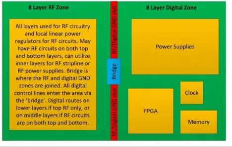
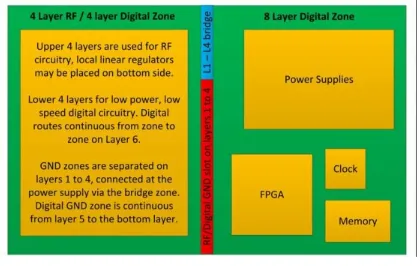
There are many times however, when the separation between circuit types is not so clear. There may be many digital control signals that require buffers, level converters or latches that need to be located close to the RF components. There may be multiple analog to digital and digital to analog converter circuits as well, and these will make the separation between domains less clear. There will even be times, quite common actually, where the RF and digital domains NEED to overlap. This is where the Z axis becomes so important. A method often used is to place RF circuitry on the top side of the board and digital circuitry on the bottom side. When this method is used, the board is divided into different zones in the Z axis, with the top four to six layers being the RF domain and the lower layers being the digital domain. Let’s say the top four layers per the 8 layer stack presented in Figure 9 below are used. Layer 1 is for RF components and signals, often with a coplanar ground flood. Layer 2 is a solid ground only. Layer 3 is power, possibly some RF stripline routes and a ground flood. Layer 4 is ground with possibly some more analog power routing. This is very often enough for the RF circuitry. So there is no reason why some digital components cannot be placed on the bottom side directly under all the RF circuitry. Digital routing and power planes can exist between layer 5 and the bottom layer, with layer 5 itself as a digital ground reference plane.
A common technique in mixed technology designs using Z axis isolation is to maximize, ( 8 mils or more ), the Z axis spacing between analog and digital ground zones, (layer 4 and layer 5 in the example stackup in figure 8), or else there may be potential for noise on the digital ground plane finding its way into the RF circuits by way of the analog ground plane. Due to the behavior of skin effect, this is not technically necessary as the energy in a properly constructed transmission line is in the dielectric between the transmission line signal trace and the reference plane, and therefore the adjacent ground planes could be as little as 3 or 4 mils apart and complete isolation in the Z axis can still be achieved. Increasing the spacing between adjacent grounds is done simply because it usually can be in the available thickness of the board, and most electrical engineers always prefer the different ground zones to be separated by as much as possible.
Notes on 8 layer Z axis isolation:
- It is common to maximize the spacing in the Z axis between the last RF ground reference plane (probably layer 4), and the first digital ground reference plane (probably layer 5). When there is a very high layer count, say 16 – 20 layers, then it is highly unlikely all those layers will be needed for digital routing directly under the RF section and it may be possible to keep one or two blank layers in the RF area under layer 4. This would make the first digital ground reference plane on layer 7 instead of layer 5, with a resulting increase in the spacing between the RF and digital ground planes.
- Consider the use of blind or buried vias to help routing digital signals on multiple layers under the RF circuitry while not allowing the vias used in the digital routing to extend above layer 5 unless those signals are needed for controlling RF devices on the top layer. This keeps the digital signals out of the RF domain and also prevents the surface ground flood and the internal ground planes for the RF circuitry from being broken unnecessarily. Energy from a digital circuit can be coupled into the RF domain through vias which penetrate the RF domain if the via stub length is long enough to resonate at one of the harmonic frequencies of the digital signals. This resonance is highest at ¼ wavelength, (in the dielectric medium), of the rise time frequency of the digital signal, and decreases significantly as the stub length decreases to a point where, at approximately 1/10th wavelength there will be virtually no
coupling into the RF domain. With typical board thickness in use there is little real chance of digital noise coupling into the RF domain through via stubs unless frequencies are well in excess of 10GHz. The use of blind and buried vias will, however, increase routing possibilities and density on the lower layers because the layout designer will not be prevented from placing a via underneath where a component pad is located on the top surface. Of course, this increases the cost of the board. There will be many times where increased density and functionality of a smaller board with blind and buried vias will outweigh the additional cost impact.
these vias makes it less likely that high speed digital noise that may be present on these signals could find its way on to the analog ground and power planes as they pass through these layers.
When Z axis isolation is used, either wholly Z axis or in combination with X/Y axis isolation, it is still possible to place some analog circuitry on the bottom layer. For example, when the design is very dense, the bottom layer may be used for placement of local linear regulators that are needed for analog and RF circuits on the top layer. This can only be done when the density of digital componentry on the bottom side is low enough to allow space for these regulators. When this bottom side analog component placement is used it is recommended that the digital power and ground planes in the lower layers of the stackup are actually used for analog power and ground in these specific areas.
This 8 layer example works well for low density digital circuitry placed behind top layer RF circuitry, where the design uses SOIC or SOT type IC buffers or other low density digital components. This type of circuitry is usually slow and low power, so the power routing for these devices can easily be accommodated on the digital routes layer (Layer 6) or the bottom layer. When there are higher density digital components and interconnect, higher layer counts will become necessary because more signal routing channels and more power planes will be required. See
Choosing Between Single And Dual Stripline
Useful RF And Mixed Technology Stackups
Isolate In X/Y Axis And Z Axis
X/Y/Z axis isolation notes:
- Blind vias may be used when making digital interconnect transitions from layer 6 to layer 8 under the RF zone, in order to keep all digital routing and noise out of the RF layers if that is seen as a requirement. (See Notes on 8 layer Z axis isolation above to determine if this is necessary). When a digital control signal needs to connect to one of the RF devices on the top side, and these are usually very slow digital signals, then a through hole via would be used to get into the RF layers above layer 4.
- Increase the distance between the RF and digital ground plane layers. – (In these examples that is layer 4 to layer 5). This stackup and isolation technique can be used for much higher speed digital circuitry if the layer 4 to layer 5 distance is large (8 mils, or more), and blind vias are used to make connections from layer 6 to layer 8. In the RF zone, the layer 4 ground and the layers above it should be drilled through only when it is necessary to connect to top side components. Many circuit boards are 62 mils thick by default, but can often be thicker. Mechanical engineering should be consulted to determine board thickness allowance as part of the process of increasing the distance between layer 4 and layer 5 in this 8 layer or any other stackup where the Z axis is used for RF to digital isolation. Fabrication must also be considered because increasing the thickness too much may cause issues with the maximum aspect ratio allowable for via holes. With higher layer count designs it may well be possible to leave one or more layers below the RF ground layer empty in the RF zone, which will effectively increase the distance between the RF and digital ground planes.
Layer 2 And Layer 3 Usage
Choosing Between Single And Dual Stripline
Useful RF And Mixed Technology Stackups
- Layers 1 through 4 are the same for all these stackups. These are where the Analog/RF circuitry is. The full use of these layers depends on how the circuitry is partitioned for isolation, in the X/Y axes, X/Y/Z axes, or Z axis only. In some cases all of the top four layers will be for Analog/RF circuitry, while in other cases they will be used partially for Analog/RF circuits and partially for digital or power supply circuits.
- The RF circuit is almost always placed and routed on layer 1 using microstrip transmission lines. No vias in the signal path. There should really be no reason why this cannot be achieved. The stackup examples show wider traces on layer 1 in the RF area. Wider traces help to reduce skin effect issues. Layer 1 is flooded with ground, and stitched to the other RF layer ground planes, wherever possible. When the surface ground flood is implemented, to avoid unwanted coplanar waveguide effects, ensure that the coplanar ground flood distance to RF traces is 3H or greater, where H is the Z axis distance to the reference ground.
- Assuming RF circuitry is placed on the top surface, then layer 2 is ground – always. - The higher layer count stackups simply allow for denser and more complex digital circuitry. Everything described above still applies. Higher layer counts simply provide more digital power and routing layers.
- Always work closely with the electrical and mechanical engineers and the fabrication vendor to determine the best way to partition and isolate different circuit zones.
- There is virtually unlimited variation in what each layer of a circuit board can be used for. The important issue with mixed technology designs is the isolation of the circuit zones, and this isolation must be taken care of at all times. This is still most commonly in X/Y axes only, but more and more in the Z axis as well, driven by the continuing need for miniaturization.
- The following stackup examples are just that, examples. Layout designers can adjust layer usage to suit their specific design needs and manufacturing processes. Stackups and layer usage are purely design dependent, and every design is different. Be creative and experiment with the use of the layers in the stackup to provide more design flexibility and better electrical results.
- Any layer can be used for any copper requirement in any area of the board. Just because layer 1 is microstrip for RF connections and layer 2 is ground in the RF zone does not mean these layers could not be used entirely differently in another area of the board.
be adapted as described above for other isolation techniques.
- It is very important to balance the stackup in the Z axis to prevent warping of the board during fabrication. This means keeping the dielectric and copper thicknesses the same from the center of the stackup to the bottom layer as they are from the center of the stackup to the top layer.
- Digital or analog components, or both, may be placed on the bottom side of the board. It is not uncommon to place the local analog power regulators below the RF circuitry on the bottom side. In some areas of the board the entire stackup may be analog/RF based regardless of how many layers are used.
- Be sure to take care in the use of vias in the digital area below the RF circuits when Z axis isolation is used. Use through vias to connect to the RF components on the surface layers but it may be better to use blind or buried vias in a digital area underneath an RF area for purely digital routes so that the digital currents can be confined to the lower half of the stackup. The same applies for any vias used to connect stripline traces in the RF zone to the surface layer, blind vias may be better because they do not penetrate into the digital layers below.
- In all cases where the top four layers are defined for RF circuitry, these can be either substituted with the bottom four layers if the RF circuitry is on the bottom side, or could be duplicated in higher layer count stackups where there may be different RF circuits on the top and bottom sides. It is even possible to build four top layers and four bottom layers for different RF circuits and four, six or eight layers in the middle for digital routing.
- In all of the following higher layer count examples, the layout designer should note that the layer usage below the RF portion, the top four layers, is entirely flexible. Layer usage presented is example usage only.
- In all of the stackup examples the analog/RF specific areas are outlined.
Routing on layers between power and ground planes:
4 Layer RF Only Design Stackup
Lyr Usage Notes
1 Analog
RF components and microstrip transmission lines. No vias in the RF signal path. With X/Y axis isolation, part of this layer is used for digital circuitry all the way through from top to bottom layers. 2 Analog Ground, always ground - except NEVER.
3 Analog
Often used for internal stripline for LO and IF signals but rarely for actual RF signal path routing. Use this layer for power distribution as well. This could also be the ground reference for layer 1 RF signals where layer 2 is too close to layer 1, which would result in thinner traces than desired.
4 Analog Contains miscellaneous non-critical signals, some power routing ifneeded and then flooded with ground.
6 Layer RF Only Design Stackup
Lyr Usage Notes
1 Analog
RF components and microstrip transmission lines. No vias in the RF signal path. With X/Y axis isolation, part of this layer is used for digital circuitry all the way through from top to bottom layers. 2 Analog Ground, always ground - except NEVER.
3 Analog
This layer would be defined for stripline RF routing with ground flood. It could still also be the ground reference for layer 1 RF
signals where layer 2 is too close to layer 1, if needed in some areas. 4 Analog RF ground plane to provide the cleanest possible striplineenvironment for layer 3.
5 Analog Power plane.
6 Analog Contains miscellaneous non-critical signals, some power routing ifneeded and flooded with ground
8 Layer XYZ Mixed RF - Digital Design Stackup – Low Density
Digital
Lyr Usage Notes
1 Mixed
RF components and microstrip transmission lines. No vias in the RF signal path. With X/Y axis isolation, part of this layer is used for digital circuitry all the way through from top to bottom layers. 2 Mixed Ground, always ground - except NEVER.
3 Mixed
Often used for internal stripline for LO and IF signals but rarely for actual RF signal path routing. Probably some local filtered power planes or power routing for RF circuit blocks.
May be the ground reference for RF signals if layer 2 is too close to layer 1 for the impedance model.
4 Mixed Ground plane. Reference for layer 3 RF traces in the RF zone anddigital ground in the digital zone.
5 Digital
Digital ground. Usually only the top four layers are needed for the RF circuitry. Increase the space in the Z axis between RF/analog ground and digital ground (layer 4 to layer 5).
6 Digital Digital control signals routing and some local digital power. 7 Digital Digital ground plane, may be entirely or partially used for digitalpower in some designs. 8 Digital Components and digital routing and some local digital power.