Ranging, and Sensing
Thesis by
Seyed Mohammadreza Fatemi
In Partial Fulfillment of the Requirements for the Degree of
Doctor of Philosophy
CALIFORNIA INSTITUTE OF TECHNOLOGY Pasadena, California
2020
Defended August 18, 2020
© 2020
Seyed Mohammadreza Fatemi ORCID: 0000-0001-9081-2608
All rights reserved
To the love of my life,
my wife Nassrin.
ACKNOWLEDGEMENTS
My first gratitude always goes to my parents who devoted their time, energy, and lives and provided me with an infinite source of guidance and love throughout my life. Every achievement I had in life was a seed they planted and nurtured. The support of my parents, my sister, and my brother gave me the courage for every step for which I am always thankful to them. I also owe a debt of gratitude to my wife, Nassrin, who stood next to me for every moment of my Ph.D. studies and was a persisting support to me. I hope that I can reciprocate at least a small fraction of the happiness and joy she brings to me.
The most precious gift in my life, that I could never appreciate enough, was being surrounded by smart people. Caltech is, of course, a unique place to pursue higher education and work towards Ph.D., but what makes it special is the people including all the faculties, students, and staff. During my years at Caltech, I had the privilege of being a member of the CHIC lab, and work with an insightful advisor, Professor Ali Hajimiri. He is not only creative, innovative, masters several subject matters, and academically brilliant, but more importantly a close friend to his students who cares about them on a personal level. I am deeply appreciative of him for everything I learned over the course of my Ph.D. as well as the friendly and warm atmosphere he created within the group.
I would like to thank all the members of the CHIC lab, in particular Aroutin Khachaturian, who is a dear friend, a great partner in technical discussions and developments, and a resourceful scientist in practice. Also, Parham Khial, who aside from being a collaborator on some adventurous project ideas was a close friend and the company of conversations about deep and fundamental research subjects.
Every member of the CHIC lab that I had the chance to be labmate with, Amirreza Safaripour, Alex Pai, Behrooz Abiri, Constantine Sideris, Aroutin Khachaturian, Brian Hong, Matan Gal-Katziri, Parham Khial, Austin Fikes, Elliott Williams, Craig Ives, Samir Nooshabadi, Oren Mizrahi, Armina Khakpour, and Ailec Wu, is a bright and unique person who contributed to my research and personal developments. I would like to express my appreciation to Professors Changhuei Yang, Kerry Vahala, Azita Emami, and Andrei Faraon for serving on my thesis committee and providing me with great feedback. There are many others to whom I owe thanks and gratitude.
While I do not have enough space to mention everyone, I will always remember them and wish them the best wherever they are.
ABSTRACT
The emergence and maturity of integrated photonic platforms over the past decade allowed for reliable integration of a large number of photonic components on a single substrate. This ability to process and control coherent light on a chip is a potential pathway for the realization of novel low-cost systems capable of non-conventional functionalities for optical wavefront engineering. In this thesis, integrated active flat optics architectures for generation, manipulation, and reception of optical wave- fronts are investigated. In particular, the application of such systems for imaging, ranging, and sensing are studied and multiple photonic systems including a large scale transmitter, a high-sensitivity receiver, and a high-resolution transceiver are demonstrated.
For generation of optical wavefronts, solutions for engineering a radiative optical waveform via emission by an array of nano-photonic antennas are studied and a chip- scale photonic transmitter is implemented. The transmitter forms an optical phased array with a novel architecture in a CMOS compatible silicon photonics process which not only dispenses with the limitations of previously demonstrated systems but also yields a narrower beamwidth leading to a higher resolution. Moreover, an integrated adaptive flat optical receiver architecture that collects samples of the incident light and processes it on-chip with high detection sensitivity is implemented.
To detect the optical samples with a high signal to noise ratio, an optoelectronic mixer is proposed and designed that down-converts the optical signals received by each antenna to a radio frequency signal in the electronic domain, provides conversion gain, and rejects interferers. This system allows arbitrary wavefront manipulation of the received signal by adapting itself to new conditions — a capability that does not exist in conventional cameras. Using this system, we realized the first high- sensitivity optical phased array receivers with one-dimensional and two-dimensional apertures and the functionality of the chips as ultra-thin lens-less cameras were demonstrated. To achieve a high-resolution integrated photonic 3D imager with low system complexity, a double spectral sampling method is developed through a special wavefront sampling arrangement on the transmitter and receiver apertures.
This transceiver architecture includes a multi-beam transmitter and a high-sensitivity receiver that can distinguish the illuminated points separately and process them simultaneously using a digital signal processor.
Moreover, novel ultra-low power architectures for generation and reception of short
RF/microwave pulses are explored. Such systems have a broad range of applications including imaging and ranging. In this study, the capability of generating and receiving orthogonal Hermite pulses of various orders using a capacitor-only time- varying network is demonstrated.
PUBLISHED CONTENT AND CONTRIBUTIONS
R. Fatemi, A. Khachaturian, and A. Hajimiri, “A nonuniform sparse 2-D large-FOV optical phased array with a low-power PWM drive,”IEEE Journal of Solid-State Circuits, vol. 54, no. 5, pp. 1200–1215, 2019. Available: https://ieeexplore.
ieee.org/document/8649827.
https://doi.org/10.1109/JSSC.2019.2896767. I designed, measured, and wrote the paper.
R. Fatemi, P.Khial, A. Khachaturian, and A. Hajimiri, “Breaking FOV-aperture trade- off with multi-mode nano-photonic antennas,” IEEE Journal of Selected Topics in Quantum Electronics, 2021. [Accepted]
I performed the theoretical developments, simulated, and wrote the paper.
R. Fatemi, B. Abiri, A. Khachaturian, and A. Hajimiri, “High sensitivity active flat optics optical phased array receiver with a two-dimensional aperture,” Opt. Express, vol. 26, no. 23, pp. 29 983–29 999, Nov. 2018. Available: http://www.
opticsexpress.org/abstract.cfm?URI=oe-26-23-29983. https://doi.org/10.1364/OE.26.029983.
I modified the design, measured, and wrote the paper.
R. Fatemi, A. Khachaturian, and A. Hajimiri, “A low power PWM optical phased array transmitter with 16° field-of-view and 0.8° beamwidth,” in 2018 IEEE Radio Frequency Integrated Circuits Symposium (RFIC), 2018, pp. 28–31. Available:
https://ieeexplore.ieee.org/abstract/document/8428847. https://doi.org/10.1109/RFIC.2018.8428847.
I designed, measured, and wrote the paper.
R. Fatemi, A. Khachaturian, and A. Hajimiri, “Scalable optical phased array with sparse 2D aperture,” in Conference on Lasers and Electro-Optics,Optical Society of Amer- ica, 2018, STu4B.6. Available: http://www.osapublishing.org/abstract.
cfm?URI=CLEO_SI-2018-STu4B.6.
https://doi.org/10.1364/CLEO_SI.2018.STu4B.6. I designed, measured, and wrote the paper.
R. Fatemi, B. Abiri, and A. Hajimiri, “An 8×8 heterodyne lens-less OPA camera,”
in Conference on Lasers and Electro-Optics, Optical Society of America, 2017, JW2A.9. Available: http://www.osapublishing.org/abstract.cfm?URI=
CLEO_QELS-2017-JW2A.9.
https://doi.org/10.1364/CLEO_AT.2017.JW2A.9. I modified the design, measured, and wrote the paper.
R. Fatemi, B. Abiri, and A. Hajimiri, “A one-dimensional heterodyne lens-free OPA camera,” in Conferenceon Lasers and Electro-Optics, Optical Society of America, 2016, STu3G.3. Available: http://www.osapublishing.org/abstract.cfm?
URI=CLEO_SI-2016-STu3G.3.
https://doi.org/10.1364/CLEO_SI.2016.STu3G.3. I modified the design, measured, and wrote the paper.
B. Abiri, R. Fatemi, and A. Hajimiri, “A 1-D heterodyne lens-free optical phased array camera with reference phase shifting,”IEEE Photonics Journal, vol. 10, no. 5, pp.
1–12, 2018. Available: https://ieeexplore.ieee.org/document/8471238. https://doi.org/10.1109/JPHOT.2018.287182.
I modified the design, measured, and wrote the paper.
TABLE OF CONTENTS
Acknowledgements . . . iv
Abstract . . . v
Table of Contents . . . ix
List of Illustrations . . . xi
List of Tables . . . xix
Chapter I: Introduction . . . 1
1.1 Contributions . . . 3
1.2 Thesis outline . . . 5
Chapter II: Integrated photonic systems . . . 7
2.1 Wavefront generation and manipulation . . . 7
2.2 Integrated silicon photonic platform . . . 9
2.3 Integrated optical phased array . . . 19
Chapter III: Large-scale sparse 2D optical phased array . . . 27
3.1 Introduction . . . 27
3.2 Silicon photonics OPA with a sparse aperture . . . 29
3.3 Aperture design . . . 33
3.4 Phase shifter network . . . 40
3.5 Phase shifter network driver . . . 45
3.6 System design . . . 54
3.7 Measurement setup and results . . . 57
3.8 Conclusion . . . 63
Chapter IV: Optical phased array receiver . . . 64
4.1 Introduction . . . 64
4.2 The theory of operation . . . 66
4.3 2D Receiver Aperture . . . 69
4.4 Optoelectronic mixer . . . 71
4.5 Design and fabrication of the OPA receiver . . . 76
4.6 Characterization and Measurement . . . 78
4.7 Conclusion . . . 84
Chapter V: Optical phased array transceiver . . . 86
5.1 Introduction . . . 86
5.2 Challenges in implementing a large scale imager . . . 89
5.3 Double spectral sampling transceiver array . . . 93
5.4 Transmitter design . . . 98
5.5 Receiver design . . . 102
5.6 Conclusion . . . 104
Chapter VI: Breaking FOV-Aperture Trade-Off with Multi-Mode Nano-Photonic Antennas . . . 105
6.1 Introduction . . . 105
6.2 Receiving photonic antenna . . . 107
6.3 Fabrication imposed limitations . . . 110
6.4 Trade-off between effective aperture and FOV . . . 115
6.5 Designing antennas beyond conventional performance limits . . . 117
6.6 Conclusion . . . 127
Chapter VII: Low power RF pulse transceiver . . . 129
7.1 Introduction . . . 129
7.2 Theoretical development . . . 130
7.3 System implementation . . . 135
Bibliography . . . 140
LIST OF ILLUSTRATIONS
Number Page
2.1 (a) Simplified schematic of a typical silicon photonics platform con- sisting a bulk silicon substrate and a buried oxide layer (BOX). Optical components are fabricated using the silicon layer on the BOX. . . 10 2.2 Single mode dielectric waveguides for 𝜆 = 1,55𝑛𝑚 wavelength (a)
Channel waveguide (b) TE mode of the channel waveguide (c) TM mode of the channel waveguide (d) Rib waveguide (e) TE mode of the rib waveguide (f) TM mode of the rib waveguide (g) A channel waveguide on a SOI silicon photonic platform. . . 12 2.3 Diagram of a (a) Directional coupler (b) Y-Splitter (c) MMI splitter . 13 2.4 Diagram of a (a) focusing grating coupler for interfacing a fiber and
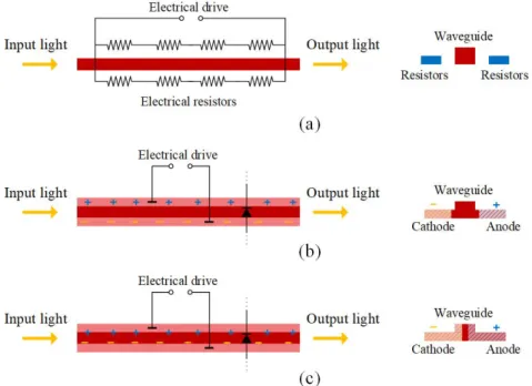
the chip (b) nano-photonic antenna with a 1D FOV (narrow in one direction and suitable for 1D OPAs )(c) nano-photonic antenna with a 2D FOV . . . 14 2.5 (a) Thermal phase shifter with electrical resistors controlling the
temperature through their power consumption. (b) PiN diode phase shifter operating in forward bias and controlling the phase shift by adjusting the current passing through the diode. (c) PN diode phase shifter operating in reverse bias and controlling the phase shift by changing the depletion region width of the diode. . . 16 2.6 (a) MZI amplitude modulator (b) Amplitude modulator without re-
flection loss (c) Ring resonator-based amplitude modulator. . . 18 2.7 (a) Cross-section of a Ge-photodiode with vertical electric field. (b)
and (c) Cross-section of Ge-photodiodes with lateral electric field. . . 19 2.8 Simplified diagram of an integrated silicon photonics OPA transmit-
ter including an input optical signal which is routed on-chip using dielectric waveguides, a power splitter tree, phase shifter network, and an array of radiating elements. . . 21
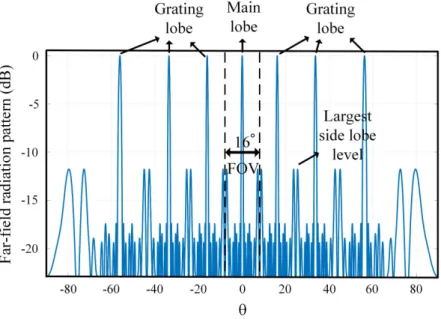
2.9 (a) An active electromagnetic surface with a continuous excitation 𝐸(𝑥 , 𝑦). The far-field radiation pattern can be calculated by breaking the surface into infinitesimal segments and count for the contribution of each segment considering its path length difference𝑙𝑥 𝑦for angles 𝜃and𝜙. (b) Far-field radiation pattern for a 4×4 uniform array with 𝑑 =1.5𝜆element spacing. . . 21 3.1 Illustration of the large inter-element spacing imposed by the optical
feed distribution as the array size scales. The excitation of the three different 2D arrays are modeled as windowed impulse trains. Fourier transform of the excitation yields the far-field pattern of the array. As the element spacing of the array increases and impulses are spaced further apart, grating lobes get more compact as the𝑠𝑐𝑎𝑙𝑖𝑛𝑔theorem predicts for Fourier transform. . . 29 3.2 (a) A 4×4 uniform array with element spacings 𝑑𝑥 and𝑑𝑦. The size
of the array with this spacing is limited to the optical feed distribution feasibility (b) A 41-element nonuniform sparse array on a 7×7 grid with the same grid spacing of𝑑𝑥and𝑑𝑦that results in the same grat- ing lobe-free steering range. Blue antennas show the non-occupied spaces on the grid. The sparse array achieves a larger scale and a better performance due to the larger number of elements. . . 32 3.3 (a) Structure of the designed compact nano-photonic antenna with
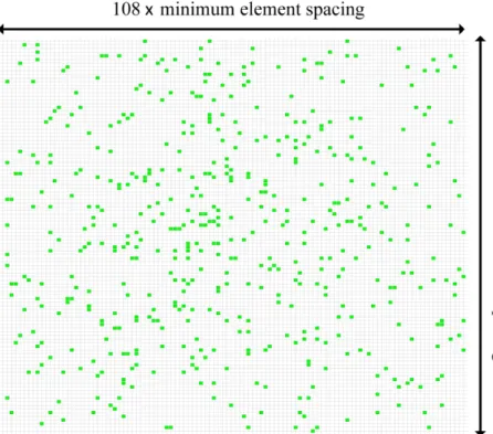
dielectric slabs as diffracting aperture (b) Far-field radiation pattern of the antenna. . . 35 3.4 Flowchart of the genetic algorithm used for sparse array design. . . . 37 3.5 The designed 128-element sparse aperture on a 729-spot grid. . . 38 3.6 The sparse aperture with embedded nano-photonic antennas and op-
tical feed distribution routing network. . . 39 3.7 Far-field radiation pattern of the designed sparse array for 𝜙=0. . . . 39 3.8 The designed 512-element sparse array aperture placed on a 11,664-
spot grid. . . 40
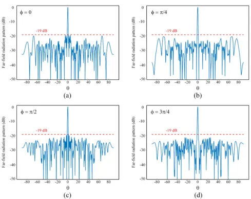
3.9 Simulated far-field radiation pattern of the 512-element sparse array with 𝜆/2 grid spacing for (a) 𝜙 = 0 (b) 𝜙 = 𝜋/4 (c) 𝜙 = 𝜋/2 (d) 𝜙 = 3𝜋/4. To illustrate more details of the pattern it is plotted for grid spacing𝜆/2 which contains all the information about the pattern, thus, including only a single lobe in the visible range. Increasing the grid spacing broadens the visible range and leads to the appearance of periodic repetition of the same pattern and grating lobes. . . 41 3.10 (a) Schematic of the designed compact spiral phase shifter (b) Ther-
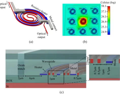
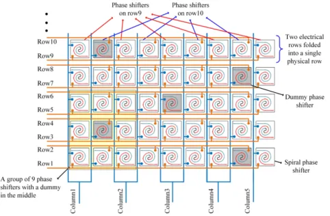
mal simulation of the phase shifter showing temperature change in and outside of the phase shifter structure (c) Cross section of the phase shifter (not to scale) showing the dimensions and sizes of the design. . . 43 3.11 The schematic of the designed folded row-column electrical access
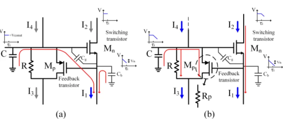
grid for the phase shifters. . . 44 3.12 (a) Schematic of a simplified PWM driver with only one transistor
switch (b) Simplified voltage drop on the switch versus time. . . 46 3.13 Stack of 5 transistors to form a high swing switch. (𝑊/𝐿)1−5 =
64𝜇𝑚/0.28𝜇𝑚, (𝑊/𝐿)6−8 = 4𝜇𝑚/0.28𝜇𝑚, 𝐶
1 = 364𝑓 𝐹, 𝐶
2 = 164𝑓 𝐹,𝐶
3=110𝑓 𝐹. . . 49 3.14 A single block of the stack (a) before activation (b) after activation. . 50 3.15 (a) Initial activation of the stack transistors through the fast path which
raises the output trigger voltage by𝑉𝑡 ℎ. (b) Full switching of the stack through the main path delivering a strong switching command after 14 ns of delay. . . 53 3.16 Simulation result for the generated PWM signals with soft turn-on
switching. The soft turn-on circuit delays the strong switching signal for 14 ns and pre-activates the stack. . . 54 3.17 Schematic diagram of the OPA chip-set and the die photos of the
fabricated chips. . . 55 3.18 (a) A single 3 dB splitter with a small footprint of the splitting region
(b) EM simulation of the 3 dB splitter showing a uniform power distribution and negligible input port mismatch (c) SEM image of the fabricated splitter (d) The 1-to-8 binary tree splitter network. . . 56
3.19 (a) Mach-Zehnder modulator for characterizing the phase shifter (b) Output power of the Mach-Zehnder modulator versus the applied voltage to the phase shifter and its corresponding phase shift. (c) Frequency response of the phase shifter. . . 58 3.20 Exemplary PWM signals generated for driving two of the rows with
two different duty cycles. . . 59 3.21 (a) Measurement setup (b) Radiation pattern of the formed beam
(the yellow spot) captured by the camera (c) Captured pattern by the camera (d) Simulated and measured results of the beam pattern for 𝜙 = 0 (e) Simulated and measured results of the beam pattern for 𝜙=𝜋/2. . . 61 3.22 (a) Illustration of the beam steering capability by forming a beam at
multiple angles (b) The letter “A” projected by beam steering. . . 62 4.1 (a) The general setting of the receiver operation (b) Free space travel-
ing distance difference between elements for a plane wave impinging at an angle(𝜃 , 𝜙). . . 67 4.2 (a) A single receiving element (b) cross section of the receiving el-
ement with detailed dimensions (c) Reception pattern of a single element,𝐺(𝜃 , 𝜙) (d) Effective aperture of the receiving element ver- sus𝜃𝑥(e) The 8-by-8 array of receiving elements. . . 70 4.3 (a) Array pattern of an 8-by-8 array with𝑑/𝜆=1.3 and(𝜃
0=0, 𝜙
0 = 0) (b) Array pattern of the designed OPA receiver for 𝜙 = 0 and (𝜃
0=0, 𝜙
0=0)(element spacing = 11.2𝜇𝑚). It is assumed that one side of the chip is blocked and light impinging on the aperture comes only from 0 ≤ 𝜃 ≤ 𝜋/2 . . . 71 4.4 (a) Block diagram of the optoelectronic mixer (b) simplified drawing
of the integrated optoelectronic mixer. . . 72 4.5 (a) Structure of the PiN diode phase shifter (b) Optical mode prop-
agating inside the phase shifter (the doped regions do not interfere with the optical mode, avoiding optical insertion loss). . . 73 4.6 (a) A simplified diagram of the receiver architecture with a 2-by-2
array aperture. (b) Photo of the fabricated chip and the building blocks. 77
4.7 (a) PiN diode phase shifter is placed in an MZI structure for charac- terizing the phase shift versus injected current (b) Output power of the MZI versus the electrical current passing through the diode, and the calculated associated phase shift of the PiN diode (c) Loss and power consumption of the PiN diode phase shifter versus electrical current passing through the diode. . . 79 4.8 Dark current of a single photodiode versus the applied reverse bias. . 80 4.9 (a) Diagram of the measurement setup (b) Measurement setup. . . 81 4.10 Measured reception pattern for various angles. . . 82 4.11 (a)-(c) Spectrum of the output signal with a 1Hz resolution bandwidth
for 20pW, 200fW, and 2fW of collected power respectively. Red curve shows the noise floor due to the shot noise of the reference signal which is adjusted to be well above the electronic noise floor to gain the maximum sensitivity (d) SNR of the detected signal versus collected incident power. . . 83 4.12 (a) Setup configuration for lens-less imaging (b) Images taken from
imaging subjects. . . 85 5.1 Conceptual schematic of 3D imaging with a LiDAR system. . . 87 5.2 (a) Fourier transform of the aperture excitation which is simplified to
one dimension (1D array)𝐸𝑓(𝑓𝑥, 𝑓𝑦) (b) . . . 95 5.3 (a) Undersampling an aperture which is tuned to form a beam does
not lead to aliasing. . . 95 5.4 Side lobe level of the transceiver with an 8-element array transmitter
and an 8-element array receiver with minimum side lobe level of
−17.85 dB . . . 97 5.5 Side lobe level of the transceiver with an 16-element array transmitter
and an 16-element array receiver with minimum side lobe level of
−24.3 dB . . . 98 5.6 A transceiver with 2-element arrays on both transmitter and receiver
sides (a) Transmitter pattern (b) Receiver pattern (c) Transceiver pattern which is the product of the transmitter and receiver patterns. . 99 5.7 A transceiver with 8-element arrays on both transmitter and receiver
sides (a) Transmitter pattern (b) Receiver pattern (c) Transceiver pattern which is the product of the transmitter and receiver patterns. . 99
5.8 (a) Schematic of the nano-photonic antenna with a 1D FOV. (b) Far- field radiation pattern of the antenna (c) The antennas are placed on a 1D array with d=15.5 µm=20λ/2 element spacing. (d) Array pattern with 21 total beams for which 10 beams fall inside the antenna FOV. . 100 5.9 (a) PiN diode phase shifter compatible with a polymer phase shifter
(b) Cross-section of the phase shifter operating in the PiN diode mode (c) Cross-section of the phase shifter after applying the polymer. . . . 102 5.10 (a) Schematic of the transmitter architecture with relative phase read-
out for the neighboring antennas (b) Die photo of the fabricated chip. 103 5.11 (a) The receiver antennas are placed on a 1D array with d=10.85 µm=20λ/2
element spacing. (b) Array pattern with 15 total beams for which 7 beams fall inside the antenna FOV. . . 103 5.12 (a) Schematic of the receiver architecture (b) Die photo of the receiver
chip. . . 104 6.1 Schematic of a standard SOI silicon photonics platform consisting a
bulk silicon substrate and a buried oxide layer (BOX). Optical com- ponents including transmit/receive photonic antennas are fabricated by patterning the silicon layer on the BOX. . . 106 6.2 Antenna setting for deriving radiation pattern in the transmit mode
and effective aperture pattern in the receive mode. Radiation pattern, 𝐷(𝜃 , 𝜙), and receiving pattern,𝐴(𝜃 , 𝜙), of an antenna in a reciprocal medium are linearly related. . . 109 6.3 (a) Radiation pattern of a transmitter antenna with−3 dB range FOV
(b) Conceptual schematic of the aperture electric field distribution, 𝐸(𝑥 , 𝑦), windowed by the aperture function,𝐴(𝑥 , 𝑦)(c)sincfunction far-field pattern of the aperture windowing effect which is equivalent to windowing a plane wave traveling in the z direction. . . 111 6.4 A conceptual side-view schematic of the transmitter antenna on a
silicon photonic platform with bottom reflections from the Box-Bulk interface and the bottom of the chip. . . 113 6.5 (a)&(b) 1D FOV antenna with 60% upward radiation efficiency
with its radiation pattern (c)&(d) Schematic of the 2D antenna with boosted asymmetry for improved performance and its radiation pat- tern achieving 80% upward radiation efficiecy. . . 114
6.6 Various forms of increasing the asymmetry to improve radiation ef- ficiency (a) using a thicker silicon layer (b) adding a specific silicon layer on the antenna (c) & (d) adding a bottom reflector. . . 115 6.7 (a) Idealized directivity pattern with FOV of𝜃 =2×𝜃𝐹 𝑂𝑉 (b)𝜂factor
versus𝜃𝐹 𝑂𝑉 that shows for an effective aperture of𝜆2, the maximum achievable FOV is 𝜃𝐹 𝑂𝑉 = 32.8◦, FOV achievable for 1D antennas in low-cost silicon photonics processes is 𝜃𝐹 𝑂𝑉 = 24.3◦ and FOV achievable for 2D antennas in low-cost silicon photonics processes is 𝜃𝐹 𝑂𝑉 =13.9◦. . . 117 6.8 (a) Multi-mode and single-mode waveguides (b) The two modes car-
ried by a multi-mode waveguide combined into a single mode. (c) Two super-modes supported by two single-mode waveguides com- bined into a single mode. (d) The power carried by a multi-mode waveguide input to a power detector that outputs the combined power.
(e) The two super-modes of the structure are input to two power de- tectors and power combining happens after down-conversion to DC.
(f) A multi-mode to multi-mode is used before feeding the power into the photodetector. . . 119 6.9 (a) Dual-mode antenna which uses two single mode waveguides to
form two super-modes carrying the optical power output by the an- tenna (b) Cross-section of the supper-modes of the antenna propa- gating in the waveguides (c) Total FOV and effective aperture of the antenna versus azimuth and elevation angles. . . 120 6.10 (a) Design parameters of the dual-mode antenna with a monotonic
FOV (b) Total FOV and effective aperture of the antenna versus azimuth, 𝜙, and elevation,𝜃, angles (c) Effective area of the antenna versus𝜃 for𝜙=0 which shows a 40° of FOV. . . 121 6.11 (a) Schematic of the designed 3-mode antenna which uses three sin-
gle mode waveguides to form the super-modes carrying the optical power output by the antenna(b) Design details of the antenna aper- ture formed by etching a binary pattern of 150 nm squares (c) Total effective aperture and individual effective aperture provided by each supported mode versus elevation angle. . . 122 6.12 A single pillar as a non-planar antenna that supports 4 mode pairs
that each pair collect power from two orthogonal polarization. . . 123
6.13 The graphs are normalized and the color bar shows the relative in- tensity (a)-(d) Modes of the polarization set 1 (e)-(h) modes of the polarization set 2 (i)-(l) Effective area of the polarization set 1 modes (effective area for the set 2 is counterpart of these graphs) (m) Col- lective effective area of set 1 (n) collective area of set 2. . . 124 6.14 (a) Dense array of pillar antennas (b) top view of the array with
dimensions of each unit cell (c)&(d) power collection efficiency of the nit cell versus azimuth angles 0° and 45° . . . 126 6.15 Power collection efficiency of the array in a 0.6 µm by 0.6 µm window
around the pillar antenna (a) azimuth angle = 0° (b) azimuth angle = 45° . . . 127 7.1 Schematic of a time-varying system and its impulse response. . . 130 7.2 (a) A base-band Gaussian pulse (b) Modulated Gaussian pulse with-
out DC component (c) Modulated Gaussian pulse with DC compo- nents (d) Modulated Gaussian pulse with many cycles. . . 135 7.3 (a) Two-capacitor time-varying circuit (b) Two-inductor time-varying
circuit. . . 136 7.4 (a) 4th order circuit for generation and reception of the first and
second order Hermite pulses with both sine and cosine carriers (b) This architecture can be extended for higher order Hermite pulses by extending the it. . . 137 7.5 A pulse transceiver system for radar ranging and imaging, as well as
data communication. . . 139
LIST OF TABLES
Number Page
3.1 Comparison Table . . . 60
C h a p t e r 1
INTRODUCTION
“The duty of the man who investigates the writings of scientists, if learning the truth is his goal, is to make himself an enemy of all that he reads, and ... attack it from every side. He should also suspect himself as he performs his critical examination of it, so that he may avoid falling into either prejudice or leniency.”
Ibn al-Haytham (Alhazen), 1021 AD
The history of pondering about light and its mysteries is entangled with the story of human kind from ancient mythologies to the earliest known philosophical studies.
Euclid and Ptolemy used geometry to explain the properties of light and believed that sight works by the eye emitting rays of light. Centuries later, Ibn Al-Haytham conducted many experiments with lenses, mirrors, refraction, and reflection, ex- plained human vision system, and showed through experiment (rather than pure philosophy) that light is an external phenomenon traveling in straight lines [1]. He also invented and quantified camera obscura, which is in fact a simple construct for manipulating a reflected light to form an image. Later, advances in engineering light with lenses and mirrors became the gateway to understand the laws of mechanics by observing celestial bodies through the works of Galileo and many others [2] while the nature of light itself remained unknown. In 1690, Christian Huygens proposed a wave nature for light based on an intuitive conviction [3], but the corpuscular theory of light supported by Isaac Newton, a scientist with immense reputation, was favored throughout the 18th century [4]. It was not until 1804 that Thomas Young's interferometric experiment shed light on the wave nature of light and helped researchers such as Augustin Fresnel to devise various other optical devises [5].
The major milestone in quantitatively describing light was taken by James Clerk Maxwell showing that light is an electromagnetic wave [6] which was followed by further research by Poincare, Kirchhoff, Sommerfeld, and many others leading to the development of Fourier optics [7]. Consequently, wavefront shaping and engi- neering using various types of lenses, mirrors, and novel optical system significantly impacted many fields of science and engineering. Within a short time after Hein-
rich Hertz provided experimental evidence for Maxwell’s equations in 1884 [8], generation, manipulation, wavefront engineering, and reception of electromagnetic waves up to the microwave region was extensively explored and a wide range of antennas and transmitter/receiver architectures have been realized [9]. However, the absence of a coherent optical source as well as fabrication platforms at nano-scale delayed the realization of similar systems in optical region of the spectrum and optical wavefront manipulation was primarily performed via lenses.
The discoveries about the particle nature of light and theoretical developments on quantum intraction of photons and atoms in the 20th century eventually led to the invention of laser in the 1960s [10], providing a coherent source of light. The invariance of the coherent light to a shift by a wavelength allows for controlling the wavefront by tuning over only a single cycle through phase wrapping. Therefore, various kinds of spatial light modulators (SLM) such as liquid crystal SLMs [11]
and MEMs based devices [12] have been developed with capabilities of modulat- ing/controlling both amplitude and phase of the optical wavefront with electrically controlled micron-sized pixels. SLMs revolutionized the display technology, intro- duced new microscopy methods, provided laser beam shaping, aberration control, and much more. Moreover, the electro-optically controlled pixels of the SLMs allowed for rapid switching between configurations leading to many novel practical optical systems such as controlled lenses, active free-space optical communications [13], and adaptive optics [14].
While designing photonic antennas similar to microwave antennas were not conven- tionally feasible due to the small optical wavelengths, advances in nano-technology, enabled by employing the light itself for photo-lithography processes, paved the way for the fabrication of miniaturized structures on various material platforms. How- ever, its impact on the electronic industry and integrated systems drew most of the attentions and investments to pursuing low cost fabrication platforms for the con- tinuously scaling transistors. While integrated electronics has revolutionized how we communicate, process data, and access information by controlling the motion of electrons, photons also played an important role in the advent of the information age by enabling the global telecommunications networks. Shortly after the invention of lasers, low loss optical fibers with 20 dB/km at 632.8 nm wavelength were demon- strated in 1970 [15] and evolved to achieve optical loss of 0.2 dB/km at 1.55 µm in the same decade [16], which is about the same value for the standard optical fibers today [17]. The unique features of optical fibers such as large bandwidth,
negligible latency, low loss, and low cross-talk allowed for the extraordinary growth in the world-wide data communication, with a record transmission capacity of over a hundred petabits per second in a single fiber of 125 µm diameter [18].
The focus on the communication industry and development of integrated silicon- based platforms led to the emergence of a new paradigm of integrated photonics on silicon-on-insulator (SOI) platforms over the past decade [19]. Designers can now integrate a large number of photonic components on a single silicon chip, and photonic foundries have become more commonplace and offer multi-project wafer (MPW) runs, which enable circuit and system researchers to explore novel photonic integrated solutions. This provides new opportunities to devise non-conventional optical wavefront manipulation techniques and a new generation of optical devices.
Efficient and low-cost on-chip waveform engineering reduces the size of many conventional optical systems by integrating many of these processes on a single chip, which in turn results in reduced cost, scalability, and higher yield. Moreover, it opens up the door for many novel applications and enables functionalities that have not been previously feasible or possible. In the future, this success of realizing reliable and low cost silicon-based integrated photonic platforms will be followed by the inclusion of other photonic materials and integration of high speed transistors along side the photonic components leading to further developments and expansion in this field.
In this thesis, active flat photonic systems implemented on integrated platforms for generation, manipulation, and reception of optical wavefronts are studied. In partic- ular, application of such systems for imaging, ranging, and sensing are considered and various photonic systems including a large scale transmitter, a high-sensitivity receiver, and a high-resolution transceiver are realized.
1.1 Contributions
In this thesis, we investigated architectures and systems to realize integrated active flat optics wavefront manipulation for imaging, ranging, sensing, and communi- cation. We studied solutions for engineering a radiative optical wavefront via nano-photonic transmitters, as well as processing incoming light on a photonic chip for directive collection and high-sensitivity detection. As a result of this research, we demonstrated a large-scale optical phased array (OPA) with a novel architecture in a CMOS compatible silicon photonic process [20]–[22]. The proposed array not only dispenses with the limitations of previously demonstrated OPAs, but also
yields a narrower beamwidth leading to a higher resolution. The proof-of-concept implementation for this architecture achieves 30 times higher resolution than the state-of-the-art 2-D OPAs. The primary benefit of such OPAs is to form an elec- tronically steerable optical beam. Forming and steering an optical beam can have a wide range of applications, such as target detection and tracking, LiDAR, optical wireless communication, image projection, and surface meteorology.
Moreover, we studied novel solutions to realize photonic receivers, demonstrating an integrated adaptive flat optical receiver architecture that collects samples of incident light and processes it on-chip with high detection sensitivity [23]–[26]. The ability to electronically control all the optical properties of an optical receiver using a compact low-cost silicon photonic chip, without any mechanical movement, lenses, or mirrors, paves the way for future generations of imagers and sensors, as well as receivers for data communication. In this system, nano-photonic antennas with large effective apertures are designed to collect samples of the incident light. It is shown analytically that under certain conditions, the incident waveform can be reconstructed using a set of captured samples and its information can be extracted. To detect the optical samples with a high signal-to-noise ratio, an optoelectronic mixer is proposed and designed that down-converts the optical signals received by each antenna to a radio frequency signal in the electronic domain, provides conversion gain, and rejects interferers. This system allows arbitrary wave-front manipulation of the received signal by adapting itself to new conditions — a capability that does not exist in conventional cameras. Using this system, we designed the first high- sensitivity optical phased array receivers with one-dimensional [24], [26] and two- dimensional [23], [25] apertures. The functionality of the chips as ultra-thin lens-less cameras was demonstrated by imaging objects through electronically steering of the main lobe (the angle with maximum directivity).
To realize a nano-photonic system for high-resolution 3D imaging applications, a transceiver architecture is devised based on a double spectral sampling technique.
This system includes a multi-beam transmitter and a photonic receiver with digital wave processing. The proposed double spectral sampling method for photonic aper- ture design enables the operation of the system with an under-sampled transmitter and receiver apertures such that information can be extracted unambiguously. The transceiver system enables high imaging resolution while maintaining a low sys- tem complexity, power consumption, and optical loss. Moreover, this architecture provides a robustness against interference, stray reflections, and clutter.
A major drawback of photonic receivers is the small collection area due to the rela- tively small number of elements as well as small fill-factor of the receiving aperture.
To devise nano-photonic antennas with high effective aperture and high FOV, we investigated the fundamental trade-offs in nano-antenna design to increase the ef- fective aperture while maintaining a large field-of-view. Multi-mode nano-photonic antennas are presented as a solution for breaking the fundamental conventional limits and accordingly various antenna structures are demonstrated.
In addition to the photonic systems, we explored new opportunities in RF and microwave integrated circuit design for pulse generation and detection. We devel- oped a family of time-varying systems that can generate arbitrary modulated/base- band pulses during the circuit transitions and detect the same waveforms through a correlation function, which is embedded in the functionality of the system. We demonstrated the capability of generating and receiving Hermite pulses of various orders using a capacitor-only time-varying network. Such a system can be used for high data-rate communications and ultra-low power applications, as well as pulsed imaging and sensing.
1.2 Thesis outline
The rest of this thesis is organized as follows: Chapter 2 introduces integrated silicon photonic platforms with a brief description of various photonic components and potential optical structures that can be fabricated on a photonic chip. Moreover, it provides an analytical setup for studying radiation from an aperture which is used in the later chapters, and presents a review of the state-of-the-art optical wavefront manipulation methods with a focus on optical phased arrays.
Chapter 3 starts with the motivations for scaling optical phase arrays as a photonic wave-front engineering technology and presents an analytical development illus- trating the trade-offs, which is followed by design and implementation of a large scale sparse OPA transmitter. In Chapter 4, the general setting of an integrated photonic receiver is explained and by utilizing the high sensitivity detection prop- erty of heterodyne detection an opto-electronic mixer is designed. The developed platform is used to realize the first functional integrated photonic receiver with phase array processing, capable of forming a reception beam and steering it electronically.
Furthermore, the functionality of this system as a lens-less camera is demonstrated.
Using these developments, Chapter 5 introduces a transceiver architecture capable of high-resolution 3D imaging. In this chapter, first the challenges in realizing a 3D
imager using integrated photonics are discussed. Then, the proposed double spectral sampling method is explained and used to extend the photonic system to a transceiver architecture, which includes a multi-beam transmitter and a photonic receiver with digital waveform processing. This chapter is followed by the design details of the implemented system. A major problem for photonic receivers is the small collection area due to the relatively small number of elements as well as small fill-factor. This is the subject of Chapter 6, which is dedicated to studying the fundamental trade-offs in increasing the effective aperture of nano-photonic antennas while maintaining a large field-of-view. Multi-mode antennas are presented as a solution for breaking the fundamental limits and accordingly various antenna structures are proposed and demonstrated.
In Chapter 7, an electronic system for generating and receiving short RF/microwave pulses is demonstrated that can be used for ranging and imaging as well as data communication. This system is based on a time-varying network that generates Hermite pulses and receives them with high-sensitivity as an analog correlator.
C h a p t e r 2
INTEGRATED PHOTONIC SYSTEMS
In this chapter, a brief survey of the existing wavefront engineering techniques in- cluding the recently developed integrated photonic systems is conducted. Moreover, the standard low cost integrated silicon photonic platforms are described with a brief discussion of various photonic structures and components that can be realized on such photonic chips. Finally, an analytical framework for studying radiation from an aperture is discussed, which will be used in later chapters, and a review of the state- of-the-art optical phased arrays as integrated photonic systems capable of forming an optical beam through controlling the radiation from an aperture is presented.
2.1 Wavefront generation and manipulation
Precise generation, manipulation, and control of the optical wavefront is required in many applications. Due to the small wavelength of optical signals, conventionally, lenses of various types, which are refractive optical elements, were the primary components used to perform wavefront adjustment and transformation. The ad- vent of the spatial light modulators (SLM) such as various kinds of liquid crystal SLMs [11] and MEMs based devices (e.g. digital micro-mirror device (DMD) [12], grating light valve (GLV) [27], etc.) provided a great deal of flexibility in mod- ulating/controlling the amplitude, phase, and polarization of the optical wavefront in both space and time on micrometer scale pixel sizes. SLM devices, which are diffractive optical elements, have been used to improve conventional optical systems as well as to devise novel optical functionalities such as high-resolution video image projection, speckle field manipulation, focusing in a complex media, tailoring the light, study of atmospheric turbulence, adaptive channel equalization in free-space communication, holographic projection, polarization control, optical trapping, and many others. These functionalities enabled various novel optical systems for ap- plications such as optical metrology [28], scanning and printing technologies, laser pulse shaping [29], projectors and holographic projection systems [30], optical infor- mation processing, optical tweezers [31], [32], automotive applications, generation of vector beams [33], microscopy [11], holographic data storage, free-space optical communication, orbital angular momentum communications [34], etc. Moreover, the ability to reconfigure SLM settings led to the emergence of adaptive optics,
which is an active field of study aiming for dynamically correcting wavefront aber- rations in order to improve the performance of optical system. However, bulky footprint, high cost, low fabrication yield, relatively large pixel size (usually in the order of several wavelengths), low reconfiguration speed, not being able to control all the parameters of light and controlling them independently, and the need for an external light source are some of the drawbacks and limitations of the current SLM technologies.
Advances in nano-fabrication over the past few decades provided the possibility of implementing micro-meter scale structures, comparable to optical wavelengths, on a thin substrate. Subsequently, there has been a rise in research on this field of flat optics to investigate photonic devices that can modify different constitutive properties of light such as wavelength, amplitude, phase, and polarization state using a large number of photonic subwavelength structures called photonic antennas [35]–
[41]. These nonidentical antennas, collectively forming a metasurface structure, capture the incident light and radiate the scattered light back into the free-space and enable the nano-scale control of the wavefront by adjusting its local amplitude, phase, and polarization. These devices were designed and demonstrated for a wide range of applications such as lenses [37], lasers [38], spectroscopy and nano-imaging [39], light emitters in LEDs [40], polarization control devices [41], etc. in both transmittive and reflective modes. Recently, active metasurface devices have also been demonstrated in which the properties of each nano-antenna are electronically adjustable [42]. The antennas on metasurface structures are the primary (and most of the times only) components that process the incident wavefront and operate independent from each other. This solo performance of the antennas which is limited to their local region significantly limits the design space and potential functionalities that can be realized.
Over the past decade, the maturity of photonic integration technologies, which were initially focused on developing higher speed optical communication links, gave birth to a new paradigm of integrated photonics. An integrated photonic platform enables fabrication of a large number of photonic components on a single chip.
Thus, coherent light can be processed on-chip through filtering, modulation, phase shift, amplitude adjustment, mode conversion, etc. to realize various functionalities that can bring about novel integrated photonic solutions. With the advent of these integrated active flat optic systems, a second type of nano-photonic antennas has emerged [43]–[46]. In this context, an antenna is defined as a transducer that couples
a guided mode into free-space mode and vice versa [20], which is the same definition used for conventional microwave antennas. In other words, an antenna is an on-chip component that in the transmitter setting is fed with a guided mode and radiates into the free-space, and in the receiver setting, captures the free-space incident wave and couples it into an on-chip waveguide. Therefore, a receiving aperture consisting an array of these antennas can be used to capture a wavefront, which is then processed and manipulated on-chip. The adjusted signals are then radiated back into the free space through a transmitter aperture with transmitter antennas [47]. This provides a greater flexibility due to the more complicated processing and avoiding the limitation of isolated and solo-performing antennas in metasurface devices. Moreover, addition of a laser source (either integrated or fed to the chip) enables the system to generate a desired wavefront with defined spatial and temporal properties. It is also possible to fully capture an incident wavefront and output its extracted features after complex detection processes on-chip.
While realization of complex systems such as 3D holographic projectors and lens- less cameras on a commercial standard level are among the potential capabilities of integrated photonic platforms, optical beamforming and steering, which needs a relatively smaller aperture, have already attracted a great deal of interest in this field.
Efficient and low cost on-chip waveform and wavefront engineering reduces the size of many conventional optical systems by integrating many of these processes on a chip which in turn results in a reduced cost, scalability, and higher yield. Since phased array processing is suitable for beamforming, active optical phased arrays with small apertures were demonstrated recently that can be used in systems such as LiDAR [48], autonomous vehicles, and point-to-point communication [49], [50].
Large-scale OPA transmitters with more than a thousand radiating elements are required to form a narrow beamwidth and high-resolution. Consequently, there have been several attempts to increase the number of elements in the array and implement functional OPA transmitters on silicon photonic platforms [43], [44], [46], [51], [52]. Since a phased array, in its general form, includes phase and amplitude control for all the radiating elements, realization of a large scale OPA opens the door for arbitrary wavefront control for more complex systems.
2.2 Integrated silicon photonic platform
Over the past decade, reliable and low cost integration of a large number (thousands) of optical components on a single silicon-based chip has become possible using various flavors of silicon-on-insulator (SOI) processes. These fabrication platforms
Figure 2.1: (a) Simplified schematic of a typical silicon photonics platform consist- ing a bulk silicon substrate and a buried oxide layer (BOX). Optical components are fabricated using the silicon layer on the BOX.
are compatible with commercial CMOS technologies, become more commonplace, and offer multi-project wafer (MPW) runs, which enable a broad range of new architectures and applications [53], [54]. The unique feature of this technology that distinguishes it from other nano-photonic systems is the possibility of designing complex systems in which many photonic components operate in harmony to process the optical signal.
Silicon photonic platforms are often based on an SOI process (Fig. 2.1) and in its simplest form have a single top silicon layer which is etched and doped to realize passive and active elements. Passive components such as dielectric waveguides, power splitters/combiners, and grating couplers transform and process the optical modes and active components such as phase shifters and optical modulators interface the optics with electronics. For a silicon-based photonic layer, these components operate at wavelengths above𝜆 =1.1 µm to maintain a low loss and avoid photon absorption due to the silicon band gap. The transfer of signals from optics to elec- tronics is realized by embedding photodetectors, which is often realized by adding a germanium layer which has a lower band gap compared to silicon. Germanium is usually added through epitaxial growth and enables efficient photon absorption for wavelengths up to𝜆 =1.8 µm. For longer wavelengths germanium become trans- parent and can be used to form optical waveguide. Most of today's low cost silicon photonic processes provide a single photonic layer, made of silicon, with multiple etch depths and doping levels used for grating coupler design and electrical access to the waveguides. This planar photonic structure presents optical routing challenges
for implementation of certain complex systems as the number of components scales.
On the other hand, multi-layer photonic platform offers multiple photonic layers that can interact with each other to realize more complex devices [55].The extra photonic layers are made of silicon-nitride [56] in some platforms which offer lower loss and a broader operational bandwidth including the visible range. However, in general, the target operating wavelength dictates the appropriate material for photonic layers.
The photonic layers are usually covered with silicon oxide and one or more metal layers are added above the photonic layers for routing and electrical interface to the devices. These metal layers contact with each other and photonic layers through inter-layer metal vias. The metal layers are usually more than 1 µm away from the photonic layers to avoid optical loss. Moreover, their low resistive loss provides the possibility of realizing traveling wave structures and microwave transmission lines along with the photonic devices. In the following, a brief description of various components that can be fabricated on such integrated photonic platforms is presented.
Photonic waveguide
An integrated photonic waveguide is one of the fundamental building blocks on integrated photonic platforms mainly used for routing and guiding the optical waves on the chip. While metallic waveguides are widely used in microwave frequencies, the high optical loss of the metals makes dielectric waveguides the suitable choice for almost all the applications. In a dielectric waveguide, the propagating optical power is confined inside the waveguide due to its higher refractive index compared to the surrounding material. While various forms of waveguides such as ridge, rib, buried, diffused, strip-loaded, and slot waveguides have been proposed for integrated photonics, rib and ridge waveguides are the most commonly used in standard silicon photonic platforms. Figure 2.2 shows a ridge (channel) waveguide which is formed by etching the photonic layer and later depositing silicon oxide that surrounds the waveguide core. Depending on its size, a waveguide can support one or multiple propagating modes. Due to the fabrication non-idealities and surface roughness of the practical implementations, there will be a random and uncontrolled mode coupling in multimode waveguides which can interrupt the operation of the photonic components. Therefore, it is desirable to adjust the dimensions of the waveguide for the target wavelength to support a single mode with low loss while prohibiting the propagation of higher order modes. However, for dielectric waveguides, there will always be a TE and a TM propagating mode. For 1.550 nm wavelength, 220 nm
Figure 2.2: Single mode dielectric waveguides for 𝜆 = 1,55𝑛𝑚 wavelength (a) Channel waveguide (b) TE mode of the channel waveguide (c) TM mode of the channel waveguide (d) Rib waveguide (e) TE mode of the rib waveguide (f) TM mode of the rib waveguide (g) A channel waveguide on a SOI silicon photonic platform.
height and 500 nm width yields a waveguide that only supports a single TE and a single TM mode. The energy of the TE mode is confined inside the structure while the TM mode will suffer high optical loss due to the surface roughness of the implemented waveguide, thus leasing to an effectively single mode waveguide. It is also possible to form rib waveguides in standard silicon photonic platforms using the etching levels provided for the photonic layer. While ridge waveguides have better confinement and lower optical loss, to control the propagation of light inside the waveguide, design modulators, and mode converters rib waveguides are more suitable.
Couplers and splitters
Couplers and splitters are passive optical components that can be used to convert optical modes and split/combine optical power from a set of inputs to a set of outputs. The most commonly used coupling mechanism on integrated platforms is evanescent coupling, which provides a low loss and efficient transfer of power from one waveguide to another. This coupling mechanism can be used to form a directional coupler which is a 4-port network as shown in Fig. 2.3(a) in which the length of the coupling region and gap spacing define the coupling ratio. Moreover, if the coupler structure is symmetric with respect to both axes, it is a hybrid directional coupler and features a 90° phase difference between its coupled and through ports.
This can be used to form a differential beat component at these two ports and form a balance photodetector (this is described in more details in section 4.4).
While a coupler can be used to split or combine optical signals with arbitrary ratios
Figure 2.3: Diagram of a (a) Directional coupler (b) Y-Splitter (c) MMI splitter
and low loss, 3-port Y-splitter and MMI (Multimode interference) couplers/splitters are other passive devices with smaller footprint which are more robust to fabrication errors and mismatches. A Y-splitter is a symmetric structure that splits the input optical power into two equal fractions by converting the input mode to the two output modes. If the optical waves are fed in the reverse direction with the same phases, perfect power combining can also be achieved. Since there is no ideal power combiner for electromagnetic waves [57], the photonic Y-splitter suffers from reflections at the input in the combining mode if there is a phase or amplitude mismatched between the two inputs.
MMI splitter/couplers are a variety of compact couplers with one or multiple in- put/output ports which are used to split or couple the power at the input ports to the output ports. These components include a multimode slab at their central part which is the section in which coupling and splitting happen by converting the single mode inputs into multimode waves and coupling back to the single mode output waveguides.
Grating couplers and nano-photonic antenna
Grating couplers are passive components with a periodic grating that modulate the spatial frequencies of the guided mode and couple it into a different direction.
These couplers are usually used to couple light from an optical fiber into the on-chip waveguides and vice versa. Figure 2.4(a) shows a focusing grating coupler which has a relatively large footprint of 50 µm by 50 µm.
Figure 2.4: Diagram of a (a) focusing grating coupler for interfacing a fiber and the chip (b) nano-photonic antenna with a 1D FOV (narrow in one direction and suitable for 1D OPAs )(c) nano-photonic antenna with a 2D FOV
In early implementations of some nano-photonic systems, focusing grating couplers have been used to couple light into free-space as well. However, more efficient nano- photonic antenna structures have been designed to radiate light in the transmitter mode and collect light in the receiver mode with defined field-of-view, directivity, and effective aperture. Nano-photonic antennas can be designed for 1D and 2D FOV, Fig. 2.4(b)-(c). More details on nano-photonic antennas and novel structures are discussed in section 6.
Phase shifter
Phase shifting is an important function for systems operating with coherent light and can be used to construct more complex functionalities such as filtering, amplitude modulation, active mode conversion, etc. There are various mechanisms available on integrated platforms to realize an adjustable phase shifter which are mainly based on changing the effective optical path length in response to an electrical control signal.
Therefore, the phase shift induced in response to an effective index change ofΔ𝑛is Δ𝜙= 2𝜋Δ𝑛 𝐿
𝜆 (2.1)
in which 𝐿 is the physical length of the phase shifter and 𝜆 is the free-space wavelength of light. SinceΔ𝑛is usually very small, in the order of 10−4, hundreds of micron length is required for the phase shifter to achieve a 2𝜋 phase shift.
There are three types of phase shift/modulation mechanisms commonly used on silicon photonic platforms which are thermal based, free carrier dispersion based, and non-linearity based. A thermal phase shifter relies on the variation of the silicon refractive index versus temperature which has a temperature coefficient of
𝛽= 𝑑𝑛/𝑑𝑇 =1.86×10⁻⁴𝐾−1[58] at a wavelength of 1.550 nm. Therefore, changing the temperature of a silicon waveguide with a length 𝐿 by Δ𝑇 results in a phase shift of 2𝜋 𝛽 𝐿Δ𝑇/𝜆. By providing enough temperature change a 2𝜋 phase shift can be achieved. On integrated systems, the local temperature of the waveguides is controlled by adjusting the drive voltage and power dissipation in an electrical resistor in the vicinity of the waveguide as shown in Fig. 2.5(a). The bandwidth of a thermal phase shifter is limited to the its thermal response, which is a function of its thermal resistance and capacitance to a colder source. While thermal phase shifters have a slower speed compared to other types of phase shifters, their optical insertion loss is negligible and makes them suitable for power sensitive applications with slow variations.
On the other hand, carrier dispersion based phase shifters can reach a high bandwidth of tens of gigahertz. This type of phase shifters induce a phase shift to a light passing in a waveguide by changing the charge (electron and holes) density in the waveguide.
The two commonly used architectures are shown in Fig. 2.5(b) and (c) which are PiN and PN diodes respectively. The PiN diode functions in forward bias and the current passing through the diode interacts with the optical mode. Changing the current changes the charge density and accordingly the phase shift per unit length.
The PN structure works in reverse bias. The reverse bias voltage level determines the width of the depletion region and accordingly the phase shift per unit length.
The third type of phase shifting mechanism is based on the optical non-linearity of the waveguide material itself. Any material reveals nonlinear behavior if it is exposed to a large field magnitude. Applying a large enough electric field across the waveguide changes its refractive index due to the contribution of the higher order polarization factors. While silicon has a symmetric crystal lattice (thus no second order non- linearity) and have a relatively small third order non-linearity, phase shifters [59]
have been demonstrated to work based on these nonlinear effects on silicon photonics platforms. The nonlinear effects are very fast and such phase shifters offer bandwidth beyond the modulating speed of electronic circuits. Moreover, the circuit model of these phase shifters is capacitive and there is no resistive power consumption.
Amplitude modulator
The amplitude modulators on integrated platforms can be categorized into two dif- ferent classes of absorption based and interference based according to their operation principle. The absorption based amplitude modulators attenuate the optical signal in
Figure 2.5: (a) Thermal phase shifter with electrical resistors controlling the tem- perature through their power consumption. (b) PiN diode phase shifter operating in forward bias and controlling the phase shift by adjusting the current passing through the diode. (c) PN diode phase shifter operating in reverse bias and controlling the phase shift by changing the depletion region width of the diode.
response to an electrical signal. Therefore, these modulators are lossy structures and suitable for applications that power efficiency is not a design concern. Moreover, in complex photonic systems that requires multiple modulators in series, the high loss of the overall architecture usually rules out the possibility of using this kind of modulators. However, absorption-based amplitude modulators usually do not need a (precise) calibration and feature high switching speed and simplicity, which makes them a suitable choice for many applications.
Since charge carriers in the light path will cause attenuation of the wave as well, the same phase modulators structures for phase shifting can be redesigned for amplitude modulation. Increasing the charge density in the waveguide increases the absorption coefficient and consequently reduces the amplitude of the output light. The modulator should be long enough to provide the desired extinction ratio.
However, the longer length translates to a larger insertion loss as well. In addition to the plasma dispersion effect, Franz-Keldysh effect is also used to realize high speed amplitude modulators by controlling the absorption coefficient of the waveguide.
Such modulators operate based on the change in the semiconductor bandgap in
response to an applied modulating electric field. On silicon photonics platforms, silicon germanium (SiGe) compound is used for this purpose and adjusting the ratio of silicon and germanium can be used to tune the modulator for the desired operation wavelength. While these modulators feature high speed and compact footprint, the extra fabrication steps needed to embed the SiGe or other materials is a drawback compared to the plasma dispersion based modulators.
The interference based amplitude modulators are formed by embedding a phase shifter into their architecture. The intensity of light at the output is a function of the phase shift experienced by the waves traveling through the modulator architecture.
The two commonly used modulators of this kind are Mach-Zehnder interferometers (MZI) and various architectures of ring resonator modulators. An MZI modulator split the input light into two paths with phase shifting capability on one or both arms (Fig. 2.6(a)). Adjusting the relative phase shifts of the two paths controls the interference at the output combiner with constructive and destructive interference in the extremes of zero phase shift and𝜋phase shift. Having phase shifters on both arms functioning deferentially can improve the performance of the modulator and reduce its form factor. The simple MZI architecture gates the optical input like an absorption-based amplitude modulator and thus introduces modulation loss. This loss can be avoided by using a directional coupler to combine the two paths at the output, Fig. 2.6(b). Moreover, this architecture provides a differential output optical signal.
The phase shifting can also be used to change the resonant frequency of a resonator.
Fig. 2.6(c) shows a ring resonator with 4 optical ports and a phase shifter that can change the resonant frequency of the ring by changing the optical path length that light travels around the ring. By moving the resonant frequency to the signal wavelength and away from it, the input light is switched between the through and drop ports. Since a resonator have a large quality factor, the resonant frequency can be shifted with relatively small phase shift. Therefore, these modulators are superior for their low voltage drive and power consumption. However, this exact same feature makes a ring resonator too sensitive to fabrication mismatches, temperature variations, and other noise and interference sources.
Photodetector
Photodetectors are electro-optical devices that convert optical signals into electrical signals (which is the reverse function of the modulators). While the low optical
Figure 2.6: (a) MZI amplitude modulator (b) Amplitude modulator without reflec- tion loss (c) Ring resonator-based amplitude modulator.
absorption of silicon makes it a good candidate for designing passive photonic com- ponents in the wavelength rages 1.1𝜇𝑚 < 𝜆 < 1.8𝜇𝑚, it is not a good photodetector for the same reason. Therefore, germanium and III/V materials have been used to form integrated photodetectors. Integration of germanium-based photodetector is compatible with CMOS electronic platforms and SiGe alloys already exists in CMOS processes. Therefore, germanium is the most common photodetector ma- terial used on silicon photonics platforms and can be integrated through chemical vapor deposition and epitaxial growth. However, there is a 4% lattice mismatch between germanium and silicon which leads to mid-gap generation-recombination
Figure 2.7: (a) Cross-section of a Ge-photodiode with vertical electric field. (b) and (c) Cross-section of Ge-photodiodes with lateral electric field.
centers and consequently increased dark current for the detector. While hybrid III/V- silicon and InGaAs-based photodetectors can potentially yield higher performance detectors (and even laser sources), the absence of fabrication methods compatible to CMOS mass production lines is a the major drawback that hampered their wide usage.
In Ge-based photodetectors, the interaction of photons and germanium generates electron hole pair which can be separated and collected by applying an electric field.
The common architectures for collecting these charges are shown in Fig. 2.2(a)-(c) with vertical and lateral field application. The germanium layer is formed on top of the silicon layer (which can be waveguides carrying light) and construct a PiN photodiodes with germanium being the intrinsic region. Since Si/Ge interface is conductive, in the vertical field structure, the germanium is doped to form a cathode, and p+ doped silicon contacts on the sides are the cathode. The relatively large refractive index of germanium causes the optical field being drawn into it and interact with germanium efficiently. Interaction length, charge swept time, recombination rate, electrical resistivity of the charge paths, etc. defines the characteristics of the photodetector. Speed, responsivity, dark current, and power handling are among the characterises that should be considered in determining the type and geometry of the photodetector.
2.3 Integrated optical phased array
An integrated optical phased array transmitter capable of electrical adaptive beam forming and steering includes a 1D or a 2D array of nano-photonic antennas [46], [60]–[62] and can be used to engineer a desired optical wavefront. The antennas are fed with phase and amplitude adjusted optical signals which are routed by on- chip dielectric waveguides, Fig. 2.8. Such an optical transmitter is suitable for applications such as LiDAR [63]–[67], point-to-point communication [68]–[70], lens-less projection [46], and holographic displays [71]. Here, we first introduce an