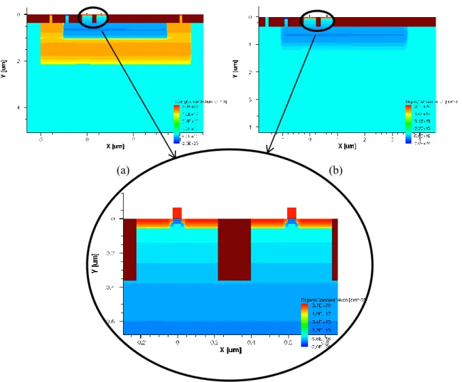
Potential in the p-well in the (a) double-well and (b) triple-well device 50 picoseconds after being hit with a particle LET of 20 MeV-cm2/mg. The potential of the p-well is higher in the three-well device than in the double-well device. Current pulse and charge collected by the second NMOS transistor (MN2) in a double- and triple-well SRAM cell after hitting the drain of the NMOSFET MN1 with an ion of LET 20 MeV-cm2/mg.
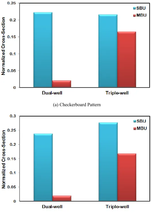
LET for double-well and triple-well devices for normal incidence irradiation with (a) checkerboard pattern and (b) ALL-0 pattern.

Triple Well Technology
Triple-well technology (described below) has many electrical advantages compared to double-well technology. In this work, the underlying mechanisms of the single event response were studied to understand in detail the response of triple well devices to ionizing radiation. The threshold voltage of a triple-well NMOS device similarly first increases with increasing implantation dose, and then decreases due to amorphization of the silicon.
The main advantage of the three-well technology is that it allows the circuits to be independent of substrate bias conditions.
Single Event Response of Triple Well Devices: Literature Review
An adaptation of the triple-well technology, described as 'merged triple-well' technology, reduces sensitivity to CMOS hatchup [15]-[16]. Although some published literature reports that the use of three-well structures is beneficial in reducing error rates, many report the opposite. It was observed that due to the collection of holes in the p-well of the triple well structure, the well becomes less biased.
They detailed the charge collection mechanisms in a 90 nm triple-well converter circuit and observed that mainly due to the p-well de-bias, the pulse widths were larger compared to double-well structures.
Charge-Sharing at advanced technology nodes
Because of these apparently contradictory results for triple-well structures, it is important to more thoroughly understand the single-event response of triple-well transistors over a wide range of particle LETs.
Overview of the work
From these simulations, triple-well technologies were found to be more vulnerable than twin-well technologies to low-LET particles, while dual-well designs were more vulnerable to moderate- and high-LET particles. Charge confinement and multi-node charge collection were found to trigger "Single Event Upset Reversal" in three-well structures, which lowers the soft fault rate compared to two-well structures at high LETs. Alpha, neutron, and heavy ion tests were performed on SRAM designs built in dual-well and triple-well technologies at 65 nm and 40 nm technology nodes to verify the obtained simulation results.
The calibration of a 40 nm commercial NMOS and PMOS transistor is described in Appendix A, and the Structure Editor and Sdevice scripts used in the simulations are included in Appendix B.
Simulation Setup
TCAD Structure
It has been found that a realistic ion trace, consistent with the theory of Kobetich and Katz (KK) [33], can have a higher charge density in the tracer core compared to the Gaussian profile commonly used in TCAD simulations. The actual ion track profile was found to be more like an exponential function than a Gaussian approximation. However, simulations performed with both a Gaussian structure and a realistic ion track structure showed saturation in SET pulse widths for 90 nm transducers [32].
In the simulations performed in this paper, the Gaussian ion track was used in conjunction with the SRH and Auger recombination mechanisms that would provide a realistic trend from the simulations in terms of the track charge density.
Summary
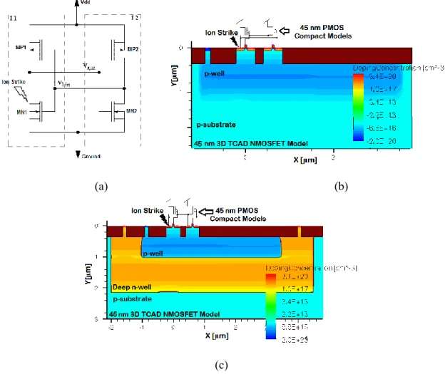
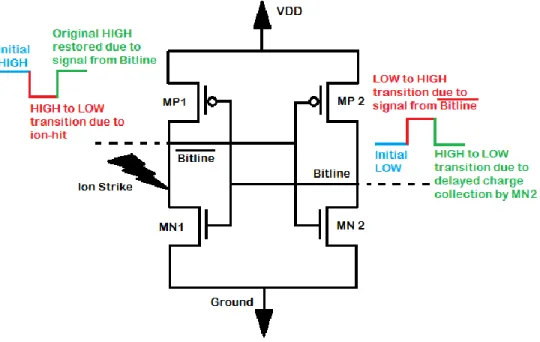
Additionally, the total charge deposited is the same with both Gaussian and realistic tracks, corresponding to the incident particle LET. In this work, the charge deposited by the incident ion is important as it would determine whether "single-event upset reversal" would trigger or not, and the ion track profile would not affect the underlying mechanisms described here. The circuit was simulated in an initial state with the output of inverter I1 HIGH and that of I2 LOW, which is due to transistors MN1 and MP2 being in the OFF state and transistors MP1 and MN2 being in the ON state.
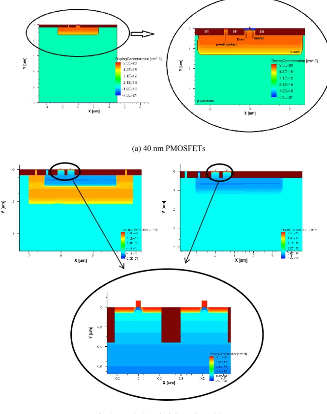
The p-well contacts of the double-well and triple-well devices are of comparable sizes.
Heavy Ion Simulations
In this chapter, an SRAM cell is simulated and the drain of the OFFNMOSFET is hit with ions. The disturbed pulses when draining an NMOSFET built into a triple-well are compared with those of a double-well. The physics behind the single-event response of double- and triple-well SRAM cells is discussed in the following section.
Mechanisms behind the Single Event Response
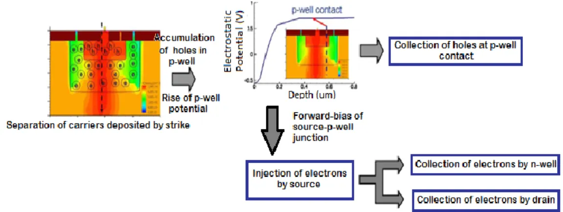
The major difference between double-well and triple-well technologies arises due to the presence of deep n-well structure in triple-well devices. In double-well technology, when a breakdown occurs, the electrons generated in the p-well are collected by the source and drain of the NMOSFET. In the case of a triple well technology, the electrons generated in the p-well as a result of the ion strike are collected by the n-well.
The large potential disturbance in the p-well in a triple-well technology due to an ion hit biases the p-well-source junction of the NMOSFET. In a double-well technology, the holes spread through the p-substrate, while in a triple-well technology, the majority of the holes are confined within the p-well. Thus, the electrostatic potential disturbance in the p-well of a p-substrate double-well technology is less than that in the p-well of a triple-well technology (Fig. 10).
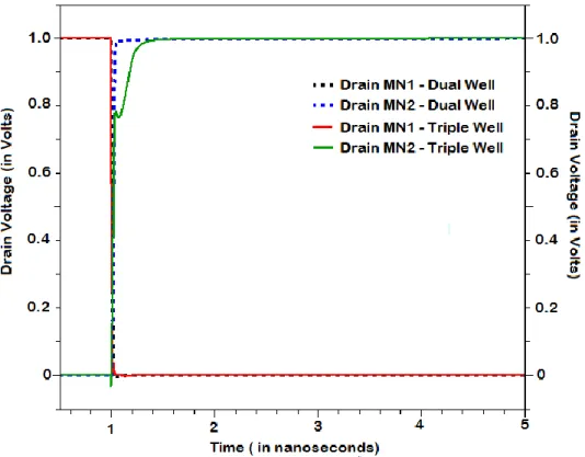
As shown in Figure 10, the substrate potential change under the NMOS transistors is much smaller in the two-well technology than in the p-well three-well technology for high-LET ion impacts. The output of inverter I2 goes from LOW to HIGH and the OFF nMOS transistor (MN2) collects the remaining charge in the p-well of the three-well system. 16 and 17 show the carrier concentration in the p-well of the double-well and triple-well system for a 25 MeV-cm2/mg LET particle impact.
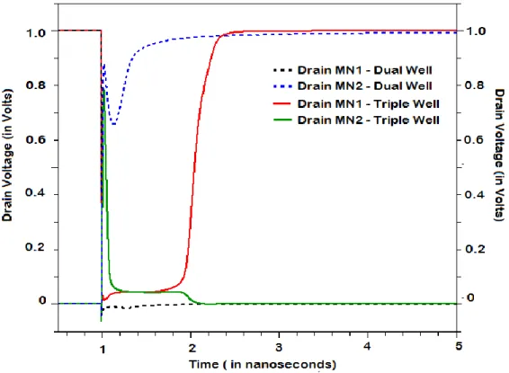
Figure 18 shows the current pulse and charge collected by NMOSFET MN2 in both the double and triple well systems for an ion strike of LET = 20 MeV-cm2/mg. The simulations were extended for very high LETs (>40 MeV-cm2/mg) for both dual- and triple-well structures. Due to the charge limitation in three-well systems, the charge cloud has a much heavier impact on transistors than in two-well systems.
23: 2D cross-section of two- and three-well NMOSFETs belonging to two different SRAM cells.
Summary
Alpha-Particle Irradiation
The design and layouts were similar, with the only difference being that one chip was manufactured in a double-well CMOS process and the other in a triple-well process technology. The thickness of the back-of-line overlay at this technology node is approximately 10 µm. It is seen that the number of faults is much less in double well systems as compared to triple well structures.
The results show that two-well SRAM cells perform better compared to three-well systems for low energy deposition.
Neutron Irradiation
The number of multi-bit failures was also higher in the case of triple-well SRAM cells. For low-LET particles, triple-well structures have a larger cross-section with soft errors. As the LET of the incident particles increases, the double-well models become more vulnerable compared to the triple-well models.
Both SBU and MBU events are lower for three-well devices compared to two-well devices for high LET particle attacks. However, at moderate to high LETs, sharing the charge of multiple nodes activates the single-event disruption mechanism observed in the previous chapter, reducing the overall error rates of the three-well NMOS transistors. Effective LET for a) two-well devices and b) three-well devices for normal irradiation and irradiation with an incidence of 30° W-E with a checkerboard pattern.
The theory developed in the previous chapter makes use of the trapped charge to reverse the disorder in triple-well SRAM cells. However, a higher number of errors is observed in the three-well SRAM cells due to the charge limitation, which has been explained in the following section. of the average number of failures) compared to the two-well structures (~76% of the average number of failures) (Fig. Due to charge confinement in three-well structures, reinforcing charge collection mechanism is predominant that reduces the soft failure rates for SRAM cells.
The single-event perturbation reversal mechanism depends on the well engineering of the three-well nMOS transistors. Thus, for high-LET particles (typically above 15 MeV-cm2/mg), three-well SRAMs do not always operate excitedly. Test results for high-LET environments show that three-well SRAM cells are less vulnerable compared to two-well SRAM cells.
Thus, for triple well technology, at high particle LETs, the soft error rate for oblique hits decreases.
Introduction
The icons on the left side indicate typical production problems; The right-hand side icons reflect the MOS scaling results based on TCAD [A1].
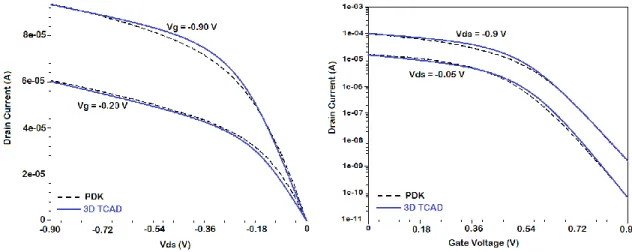
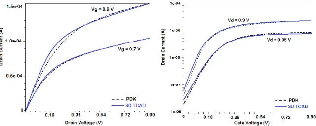
Problem: Calibration of Device Models
Approach: Commercial 40 nm Device Cross Sections
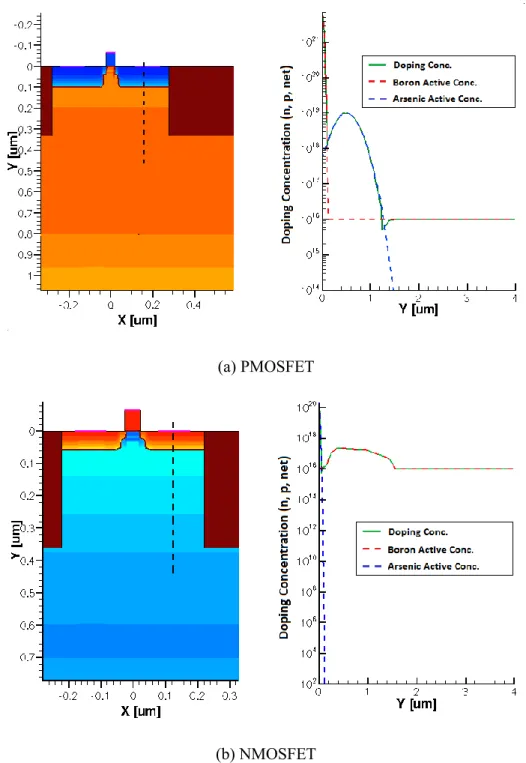
The doping profiles in the channel were largely determined by iterative methods during the DC calibration process. The channel implant structure consisted of a threshold implant on the surface, which is used to adjust the device threshold voltage (Vt). To flank the lightly doped shallow drain (LDD) extensions on both the source and drain sides, two small regions of doping are known as "halo-doping".
From a calibration perspective, this provides a control over the subthreshold slope without significantly changing the threshold voltage. For the lightly doped drain extensions (LDD), dimensions and doping levels determine the series resistance of the device, which has a significant effect on the peak driving strength of the device. Once these factors were determined through a lengthy iterative comparison of the device characteristics with those in the paper, the effective channel length came to about 34 nm.
Doping Profiles of Devices
It was assumed that similar well and substrate profiles were used for the 45 nm devices. For the fine structure of the channel doping and LDD profiles, we select a number of cut lines at different locations.