Chapter 2
2D Materials as protective layers on silicon photoanodes
This chapter has been adapted from the following citation. Further permissions related to the material excerpted should be directed to the ACS.
Thompson, A. C. et. al. (2016). “Lightly Fluorinated Graphene as a Protective Layer for n-Type Si(111) Photoanodes in Aqueous Electrolytes”. In: Nano Letters, 16(3), pp 4082-4086.
https://pubs.acs.org/doi/abs/10.1021/acs.nanolett.6b00773
Several protective coating strategies have been developed to suppress
deleterious surface reactions associated with corrosion or passivation of semiconductor photoanodes in aqueous electrolytes.1-2 NiOx films prepared by reactive sputtering or amorphous TiO2 films in conjunction with a Ni-oxide based electrocatalyst have
produced extended stability for Si photoanodes and allow the photochemical evolution of O2(g) from water under alkaline conditions.3-4 Thin metallic overlayers or transparent conductive metal oxide protective layers often result in relatively low photovoltages due to thermionic emission of majority carriers at Si/overlayer Schottky contacts.3-10
Insulating metal oxide barriers must be thin enough (a few nm) to permit conduction by tunneling, and such thin layers are difficult to prepare in a pinhole-free manner over macroscopic areas.5, 11-12 Chemical functionalization has led to improved stability of n-Si surfaces, but such methods have not yet yielded stability over extended time periods in aqueous electrolytes.13-15
An ideal protective coating would be transparent, provide low resistance to charge transfer, allow for maximum energy-conversion efficiency for a range of
semiconductor/electrolyte contacts, would be applied easily to semiconductor surfaces, would be capable of uniformly protecting macroscopic electrode areas, and would be chemically and electrochemically stable under the relevant conditions. Monolayer graphene can be prepared in large (>100 cm2), pinhole-free layers and transferred to any arbitrary planar surface, and has been shown to inhibit oxidation of metals both in air
and in aqueous solution.16-21 Graphene is chemically inert, optically transparent, can be deposited onto surfaces at room temperature. Illuminated graphene-coated Si
photoanodes in contact with neutral pH aqueous electrolytes have demonstrated stability for over 1000 s while providing desirable photoelectrochemical performance.22-25
However, the graphene does not completely protect the Si photoanodes from oxidation, and the devices exhibit partial Fermi-level pinning which limits their energy-conversion efficiency. The incomplete protection and Fermi-level pinning are consistently ascribed to reactive sites near grain boundaries in the polycrystalline graphene produced by chemical-vapor deposition (CVD), and to the presence of mid-gap electronic states introduced at the n-Si/Gr interface as a result of the graphene electronic structure, respectively.
Relative to unfluorinated graphene, fluorination of graphene should reduce the density of states near the Fermi level, thus reducing Fermi level pinning effects, and should passivate reactive graphene defect sites via fluorine capping.26-28 Accordingly, we report herein an investigation of the stability and photoelectrochemical behavior of fluorinated-graphene-coated Si photoanodes in contact with aqueous electrolytes.
Methods
Materials
Single-crystalline, Czochralski grown, (111)-oriented, planar, 380 μm thick, phosphorus doped, 1.1 Ω-cm resistivity (doping density, ND ≈ 5x1015 cm-3) single-side polished n-type silicon wafers were obtained from University Wafer, Inc. Water was obtained from a Barnstead Nanopure system and had a resistivity ≥ 18.0 MΩ-cm.
Copper Etch Type CE – 100 (FeCl3-based, Transene Company, Inc., Danvers, MA), and buffered HF(aq) (semiconductor grade, Transene Company, Inc., Danvers, MA) were used as received. Acetone (HPLC grade, Sigma-Aldrich) was used as received.
Acetonitrile (99.8% anhydrous, Sigma-Aldrich) used in electrochemical measurements was dried over Al2O3 prior to use.
Ferrocene (Fc, bis(cyclopentadienyl)iron(II), 99%, Strem), cobaltocene (CoCp2, bis(cyclopentadienyl)cobalt(II), 98%, Strem), and acetylferrocene (AcFc,
(acetylcyclopentadienyl)-cyclopentadienyl iron(II), 99.5%, Strem) were purified via sublimation. Ferrocenium tetrafluoroborate (Fc+[BF4]- , bis(cyclopentadienyl)iron(III) tetrafluoroborate, technical grade, Sigma-Aldrich) was recrystallized from a mixture of diethyl ether (ACS grade, EMD) and acetonitrile (ACS grade, EMD) and dried under vacuum. Cobaltocenium hexafluorophosphate (CoCp2+, bis(cyclopentadienyl)cobalt(III) hexafluorophosphate, 98%, Sigma-Aldrich) was recrystallized from a mixture of ethanol (ACS grade, EMD) and acetonitrile (ACS grade, EMD) and dried under vacuum.
Acetylferrocenium (AcFc+) was generated in situ via electrochemical oxidation of AcFc0 with the concomitant reduction reaction occurring in a compartment that was separated by a Vycor frit from the working electrode compartment. Potassium ferricyanide
(K3[Fe(CN)6], 99.2%, Sigma-Aldrich) and potassium ferrocyanide (K4[Fe(CN)6]•3H2O, ACS Certified, Fischer Scientific) were used as received. LiClO4 (battery grade, Sigma- Aldrich) was used as received. Petri dishes used were Falcon Optilux™ branded and were cleaned with water prior to use. All other chemicals were used as received unless otherwise noted.
Electrode fabrication
Monolayer graphene was grown by chemical-vapor deposition (CVD) of carbon on Cu.29 Additional CVD-grown monolayer graphene on Cu was purchased from Advanced Chemical Supplier Materials. A 2.5 cm x 1 cm piece of monolayer graphene on Cu (from either source) was fluorinated using a home-built XeF2 pulse chamber, with one pulse of XeF2 (g) at 2 Torr for 90 s with a base pressure of <1 mTorr.28 X-ray photoelectron spectroscopy (XPS) of the resulting F–Gr confirmed the fluorination.27-28
The F–Gr was further characterized by UV/Vis and Raman spectroscopy. The fluorinated graphene samples on Cu were then coated with 495K A4 polymethyl methacrylate (PMMA, MicroChem) by spinning at 2000 rpm (500 rpm s-1 acceleration) for 60 s, followed by a 5 min bake at 185 °C. This procedure was repeated twice to yield a PMMA/F-Gr/Cu stack.
Smaller pieces were cut from the PMMA/F-Gr/Cu and floated in FeCl3 solution until complete removal of the Cu (~1 h) was observed. To remove the etchant residue, each stack was transferred between five consecutive ≥18MΩ-cm resistivity water baths.
N-type Si was etched for 30 s in buffered improved HF (Transene) to yield n-Si–H surfaces, and any SiO2 was removed using a modified SC1/SC2 cleaning method. SC-1 consisted of soaking the Si wafers in a 5:1:1 (by volume) solution of H2O, NH4OH (~30 wt.%, J.T. Baker) and H2O2 (~35 wt.%, Sigma) for 10 min at 75oC. After washing with H2O, SC-1 cleaned wafers were exposed to SC-2 conditions, which consisted of soaking the Si wafers in a 5:1:1 (by volume) solution of H2O, HCl (11.1 M, Sigma) and H2O2 (~35 wt.%, Sigma) for 10 min at 75 oC. A clean PMMA/F-Gr stack was then pulled gently onto the appropriate Si wafer and dried with a stream of N2(g) to remove any remaining water between the Si wafer and the graphene sheet. The final PMMA/F-Gr/wafer stack was baked at 80 °C for 10 min in air. The majority of the PMMA was detached with a 10 min acetone soak and the remaining PMMA residue was removed by an anneal (H2:Ar v:v 5:95) for 2h at 350°C.30
Si/F-Gr electrodes were fabricated using Ga:In (75:25) eutectic as an ohmic back contact. The wafers were attached to a Cu wire with Ag paint (high purity, SPI
Supplies).29, 32 All surfaces except the F–Gr layer were covered with insulating epoxy (Loctite Hysol 9460). CH3-terminated Si(111) wafers were prepared using a previously reported procedure.31 H-terminated Si(111) electrodes were etched with HF(aq) immediately before use.
Instrumentation
X-ray photoelectron spectroscopic (XPS) data were collected at ~5 × 10⁻⁹ Torr using a Kratos AXIS Ultra DLD with a magnetic immersion lens that consisted of a spherical mirror and concentric hemispherical analyzers with a delay-line detector (DLD).
An Al Kα (1.486 KeV) monochromatic source was used for X-ray excitation. Ejected electrons were collected at a 90° angle from the horizontal. The CASA XPS software package v 2.3.16 was used to analyze the collected data.
Raman spectra were collected with a Renishaw Raman microscope at =532 nm through an objective with numerical aperture=0.75. The laser power was ~ 3 mW.
UV/Vis transmission spectra were collected with a Cary 5000 absorption spectrometer equipped with an external DRA 1800 attachment. The data were
automatically zero/baseline corrected by the instrument before any additional processing was performed.
Electrochemical data were obtained using a Princeton Applied Research Model 273, Biologic SP-250, or a Gamry Reference 600 potentiostat. A Pt wire reference electrode (0.5 mm dia., 99.99% trace metals basis, Sigma-Aldrich) and a Pt mesh counter electrode (100 mesh, 99.9% trace metals basis, Sigma-Aldrich) were used for the electrochemical measurements. The cell potentials for the nonaqueous redox species were determined using cyclic voltammetry to compare the solution potential to the formal potential of the redox species. The potential difference between cells was calculated using the difference between the formal potentials for each redox couple in conjunction with standard reduction potentials from the literature. The CH3CN-CoCp2+/0
solution (CoCp2 [3 mM]/ CoCp2+ [50 mM]) was calculated to have a solution potential of E(A/A-) = -1.26 V vs Fc/Fc+, the CH3CN-Fc+/0 solution (Fc [55 mM]/ Fc+ [3 mM]) was calculated to have E(A/A-) = -0.10 V vs Fc+/Fc, and the CH3CN-AcFc+/0 solution (pre- electrolysis AcFc concentration = [50 mM]) was calculated to have E(A/A-) = +0.40 V vs
Fc+/Fc. The nonaqueous electrochemical solutions each contained 1.0 M LiClO4. The aqueous 50 mM K3[Fe(CN)6] - 350 mM K4[Fe(CN)6] solution contained no additional supporting electrolyte due to the high intrinsic salt concentration. The current under forward bias saturated at much larger values in the Fe(CN)63-/4- solution than in the Fc+/Fc solution due to the increased concentration of electron-accepting species in the Fe(CN)63-/4- solution. Fc[BF4] is a highly colored species that, at high concentrations, absorbs a significant fraction of the light prior to photons striking the photoelectrode. The electrolyte solution was rapidly stirred with a small, Teflon-covered stir bar. Illumination was provided with an ENH-type tungsten-halogen lamp. Illumination intensities were set to provide ~10-11 mA cm-2 of light-limited current density. These intensities
corresponded to ~1/3rd of a Sun (~33 mW cm-2), respectively, as determined through the concurrent use of a Si photodiode (Thor Laboratories) that was calibrated relative to a secondary standard photodetector that was NIST-traceable and calibrated at 100 mW cm-2 of AM1.5G illumination. Nonaqueous electrochemistry was performed anaerobically in an Ar(g)-filled glovebox. Aqueous electrochemistry was performed in air. Electrodes were washed with H2O and dried prior to transfer between electrolyte solutions.
The current density versus potential data in HBr(aq) were measured using a three-electrode setup with a Si working electrode, a Pt wire pseudo-reference electrode, and a large Pt mesh counter electrode. The electrolyte consisted of aqueous 0.4M Br2 - 7.0 M HBr (pH=0) electrolyte under rapid stirring, and ~33 mW cm-2 of simulated solar illumination from an ELH-type W-halogen lamp.
Photoelectrochemical deposition of Pt was performed by immersing the electrode into an aqueous solution of 5 mM K2PtCl4 (99.9%, Alfa Aesar) and 200 mM LiCl. Using a three-electrode setup, with a saturated calomel reference electrode and a Pt mesh counter electrode, galvanostatic control was maintained at -0.1 mA/cm2 in a stirred
solution until -100 mC/cm2 had passed. The samples were then rinsed with deionized water and were dried under a stream of N2(g).
The stability of the fluorinated graphene was tested under acidic, neutral, and alkaline aqueous solutions, respectively. To insure that the same area was examined before and after testing, a small area on the graphene wafer was outlined with Hysol 9460 epoxy. Optical images along with Raman spectra were acquired, and wafers were then placed for 1 h in aqueous solutions at pH 0, pH 7, and pH 14. After carefully rinsing the samples with >18 MΩ-cm H2O and drying the samples with a stream of N2(g), optical images along with Raman spectra were obtained from the same areas as done before testing.
Results
Characterization
Figure 1 shows the x-ray photoelectron spectra and Raman spectroscopy of n- Si/F–Gr samples before and after the final anneal under forming gas. The C 1s region before annealing displayed four peaks at binding energies of 284.8 eV, 285.6 eV, 287.2 eV, and 289.5 eV, attributed to C–C, C=C, C–O, and C–F bonds respectively. The F 1s region displayed two peaks at binding energies of 687.1 eV and 690.0 eV,
corresponding to ionic and covalently bound fluorine atoms. The Raman spectra before annealing showed characteristic graphene peaks at 1585 cm-1 and 2690 cm-1 known as the G and 2D peak respectively. Fluorination also leads to the presence of a prominent defect peak at 1350 cm-1.
After annealing, two additional peaks, at 291 eV and 293.5 eV (inset), attributable to CF2 and CF3 groups, were observed in the C 1s XP spectra. The positions of the peaks in the F 1s region were shifted slightly to 686.1 eV and 689.8 eV, respectively, and decreased in size. The defect peak at 1350 cm-1 is still visible underneath a new broad peak corresponding to the presence of amorphous carbon on the surface. These spectra are consistent with a lightly fluorinated (CXF, x>10) graphene surface.4 The change in fluorination profile after annealing is consistent with a reorganization of the fluorine on the surface, and the XPS spectra demonstrate the expected decrease in fluorine content after a two-hour 350 °C anneal under a H2:Ar (5:95) atmosphere.4
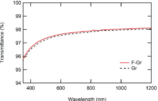
Further characterization after annealing by UV/Visible spectroscopy is shown in Figure 2 for both Gr and F–Gr. Both materials transmit 97% of incoming light on average across the region from 350 nm to 1200 nm. While transmittance decreases at shorter wavelengths for both, no increase indicative of the presence of a bandgap was detected.
The small change in transmittance at 800 nm marks the region where the instrument switches the grating used for collection.
Figure 1. Raman and X-ray photoelectron (XP) spectra of fluorinated graphene (F–Gr) before and after annealing. (A) The C 1s region before annealing. Peaks attributed to carbon bound to fluorine are shown in green; peaks attributed to carbon bound to carbon are shown in blue; and peaks attributed to carbon bound to oxygen are shown in red. (B) The F 1s region before annealing. (C) The Raman spectrum of before annealing. The prominent defect peak is visible at 1350 cm-1. (D) The C 1s region after annealing. Two new CFx peaks are visible. (E) The F 1s region after annealing. The two peaks are shifted slightly down in energy from the original sample. (F) The Raman spectrum after annealing. The defect peak is visible under a broad peak corresponding to amorphous carbon.
Figure 2. UV/Vis spectra of Gr and F-Gr on glass. Graphene and fluorinated graphene were transferred to borosilicate glass slides using the standard transfer procedures (vide supra).
Electrochemical stability
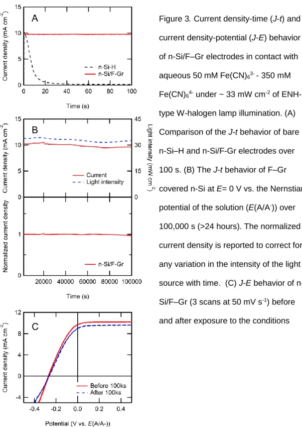
Figure 3 shows the current-density versus time (J-t) and current density vs.
potential (J-E) behavior for illuminated (~33 mW cm-2 ENH-type W-halogen lamp) n-Si/F–Gr photoanodes in contact with aqueous 50 mM Fe(CN)63- - 350 mM Fe(CN)64-
(aq). The n-Si/F–Gr electrodes exhibited stable current over 100 s while the current density of n-Si–H electrodes decayed to nearly baseline values over the same time period (Figure 3a). Furthermore, the current density of the n-Si/F–Gr electrode decayed by less than 1 mA cm-2 for > 100,000 s of continuous operation (Figure 3b). After correcting for fluctuations in the light intensity impinging on the electrode, greater than 97% of the expected current density of an ideally stable electrode was observed. Figure 3c depicts the J-E behavior before and after exposure to the conditions in Figure 3b. The stable open-circuit potential (-0.27 V vs. E(A/A-)) and fill factor (0.33 before exposure, 0.32 after exposure) show relatively little change in the n-Si/F–Gr interface.
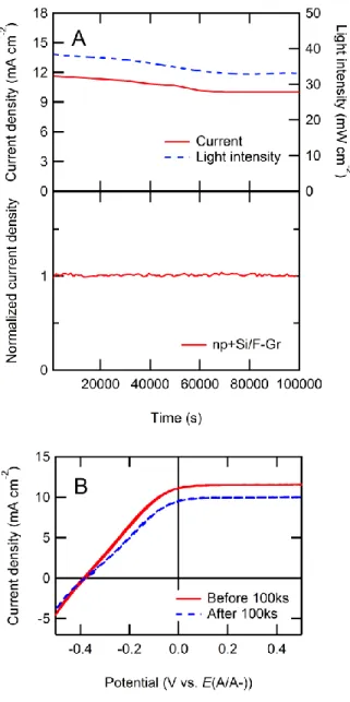
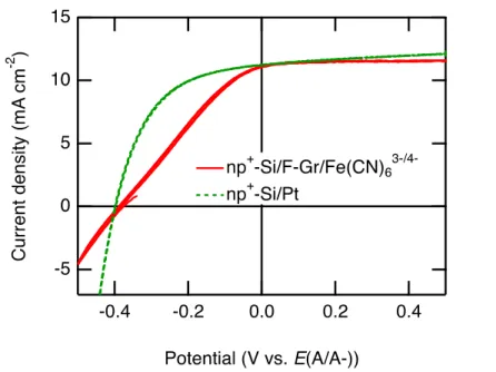
Similar results were observed for np+-Si/F–Gr electrodes (Figure 4). For the np+- Si/F-Gr/Fe(CN)63-/4- cell, the following photovoltaic metrics were measured: Voc = -0.39 V, Jsc = 11.1 mA cm-2, ff = 0.30. The same degree of stability is seen with no decrease in photocurrent over 100,000 s. Additional data were collected with a Pt catalyst to demonstrate that the fluorinated graphene overlayer did not attenuate the effect of a catalyst on fill factor (Figure 5). For the np+-Si/Pt PV cell, the following photovoltaic metrics were measured: Voc = -0.40 V, Jsc = 11.3 mA cm-2, ff = 0.50. The similar Voc
values with varying fill factors between these two interfaces suggest that the Si/F- Gr/Fe(CN)63-/4- interface is the source of an additional series resistance but that the parallel shunt resistances are similar between the np+-Si/Pt and np+-Si/F-Gr/Fe(CN)63-/4
interfaces. A similar parallel shunt resistance is also consistent with the use of the same buried photoactive junction at each interface. The np+-Si/Pt PV cell was prepared by
evaporating 15 nm of Pt onto the freshly HF etched p+ surface of an np+-Si chip and scribing a GaIn eutectic onto the backside of an n-doped surface.
Figure 3. Current density-time (J-t) and current density-potential (J-E) behavior of n-Si/F–Gr electrodes in contact with aqueous 50 mM Fe(CN)63- - 350 mM Fe(CN)64- under ~ 33 mW cm-2 of ENH- type W-halogen lamp illumination. (A) Comparison of the J-t behavior of bare n-Si–H and n-Si/F-Gr electrodes over 100 s. (B) The J-t behavior of F–Gr covered n-Si at E= 0 V vs. the Nernstian potential of the solution (E(A/A-)) over 100,000 s (>24 hours). The normalized current density is reported to correct for any variation in the intensity of the light source with time. (C) J-E behavior of n- Si/F–Gr (3 scans at 50 mV s-1) before and after exposure to the conditions
Figure 4. Current density vs. time (J-t) and current density vs potential (J-E) behavior of np+-Si/F–Gr electrodes in contact with aqueous 50 mM Fe(CN)63-
- 350 mM Fe(CN)64- electrolyte under
~33 mW cm-2 of ENH-type W-halogen illumination. (A) The J-t behavior of np+-Si/F–Gr at E= 0 V vs. E(A/A-) over 100,000 s (>24 h). The
normalized current density is reported to correct for any variations in the light intensity during the experiment. (B) J- E behavior of np+-Si/F–Gr (3 scans at 50 mV s-1) before and after exposure to the conditions depicted in (A). The current density decay in the original chronoamperograms is consistently ascribed to fluctuations in the light source, as well as to decomposition of the Fe(CN)63-/4- under illumination, which produced thin colored film on the electrochemical cell over the course of the experiment depicted in (A).
Figure 5. J-E behavior of an np+-Si/Pt PV cell and an np+-Si/F-Gr/Fe(CN)63-/4-
photoanode under ~33 mW cm-2 of ENH-type W-halogen illumination. For this cell, the (E(A/A-)) referenced on the x-axis refers to the potential of the Pt contact.
Table 1. |Voc| values for n-Si/Gr and n-Si/F–Gr electrodes in contact with non-aqueous redox couples under ~33 mW cm-2 of W-halogen illumination. The Nernstian potential, E(A/A-), of the contacting non-aqueous electrolytes were measured as follows:
E(CoCp2+/0) = -1.26 V vs. E°’(Fc+/0), E(Fc+/0) = -0.1 V vs. E°’(Fc0/+), E(AcFc+/0) = +0.4 V vs E°’(Fc+/0).
|Voc,CoCp2+/0| (V vs.
E(CoCp2+/0)
|Voc,Fc+/0| (V vs.
E(Fc+/0)
|Voc,AcFc+/0| (V vs.
E(AcFc+/0)
Gr 0 0.26 0.43
F–
Gr 0 0.20 0.30
The behavior of n-Si/Gr and n-Si/F–Gr in contact with a series of non aqueous, one-electron redox couples spanning a range of potentials is shown in Table 1. The n- Si/Gr samples consistently showed no photovoltage in contact with cobaltocene (CoCp2+/0, -1.26 V vs. E°’(Fc+/0)) and increasing values for photovoltage in contact with more positive couples, such as ferrocene (Fc+/0, -0.1 V vs. E°’(Fc0/+)) and
acetylferrocene (AcFc+/0, +0.4 V vs E°’(Fc+/0)). The same trend was observed for the n- Si/F–Gr samples, although the photovoltages were attenuated from those of the n-Si/Gr samples.
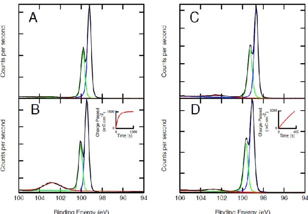
Figure 6 shows a comparison of the XP spectra of methyl-terminated n-Si electrodes (n-Si–Me) with and without a F–Gr protective layer before and after photoelectrochemical testing in an aqueous 50 mM Fe(CN)63- - 350 mM Fe(CN)64-
electrolyte. After passing 1600 mC cm-2 of anodic charge on an n-Si-Me electrode, the growth of an oxide peak was observed in the Si 2p XPS region. In contrast, no
Figure 6. XP spectra of n-Si–Me and n-Si–Me/F–Gr electrodes. (A) and (B) show the XP spectra of an n-Si–Me electrode before and after passing 1600 mC cm-2 (inset) while passing anodic current in contact with an aqueous 50 mM Fe(CN)63- - 350 mM Fe(CN)64-
electrolyte. (C) and (D) show an n-Si–Me/F–Gr electrode before and after passing 3200 mC cm-2 under similar electrochemical conditions to (A) and (B).
additional growth of the oxide peak was observed after passing twice the number of Coulombs (3200 mC cm-2) across an n-Si–Me/F–Gr electrode.
XPS analysis was performed in order to determine the effect of electrochemical oxidation at the Si–Me surface on the oxidation state of the Si photoanode surface (Figure 6). Silicon oxide detected before and after electrochemical oxidation was quantified using a simple substrate—overlayer model described by equation 1:8
𝑑 = 𝜆𝑜𝑣sin 𝜃 {ln [1 +𝐼𝑆𝑖𝑜
𝐼𝑜𝑣𝑜 ∗𝐼𝑜𝑣
𝐼𝑆𝑖]} (1)
Where d is the overlayer thickness, λov is the attenuation factor through the oxide overlayer (assumed to be 2.6 nm)9, 𝜃 the angle from the surface of the sample to the detector (90°), 𝐼𝑆𝑖
𝑜
𝐼𝑜𝑣𝑜 is an instrument normalization factor related to the expected signal for a pure Si and a pure SiO2 sample (taken to be 1.3 for this instrument), Iov is the
measured intensity of the silicon, and Iov is the measured intensity of the silicon oxide overlayer. The thickness of a monolayer of oxide was taken to be 0.35 nm.10 Negligible silicon oxide was detected on the bare methyl-terminated silicon surfaces prior to electrochemical oxidation (Figure 6a) and an oxide thickness of approximately 0.75 nm, or >2 monolayers of oxide, was observed after exposure of the Si–Me surface (Figure 6b) to the electrochemical oxidation conditions described in Figure 6. An oxide thickness of approximately 0.15±0.05 nm was detected on the Si–Me/F–Gr surfaces prior to electrochemical oxidation (Figure 6c) and an oxide thickness of approximately 0.17± 0.5 nm, was observed after exposure (Figure 6d) of the Si–Me/F–Gr surface to the electrochemical oxidation conditions described in Figure 6. Hence, F–Gr acts as a physical barrier to oxide formation, preserving the photoelectrochemical behavior of the n-Si-Me/solution interface. Methylated surfaces were used because, in contrast with n- Si–H surfaces, the n-Si–Me surface does not easily oxidize in air or form significant
oxide upon fabrication of n-Si/F–Gr interfaces, allowing more facile observation of oxide growth in the presence of various protective layers, such as F–Gr.
The photoelectrochemical stability of pristine graphene-coated n-Si electrodes and of fluorinated graphene-coated electrodes was compared by collecting J-t data for n- Si/Gr and n-Si/F–Gr electrodes from four different electrode ‘batches’ (two n-Si/Gr and two n-Si/F–Gr batches) in contact with aqueous 50 mM Fe(CN)63-- 350 mM Fe(CN)64-
under ~33 mW cm-2 of ENH-type W-halogen illumination (Figure 8). These batches of electrodes each mutually consisted of 5-6 electrodes in which each electrode was fabricated from the same section of a larger sheet of Gr or F–Gr, respectively. However, between batches of electrodes, different PMMA/(F–)Gr/Cu stacks or different regions of the same stack were used. The n-Si/Gr from the first graphene electrode batch (batch Gr_A) exhibited stable current densities for > 1000 s (Figure 8a). Among these
electrodes fabricated, all five electrodes were photoelectrochemically stable (5/5 stable, where stability was defined as having a current density at t=1000 s of at least 60% of the current density displayed at t=0 s). This definition was used because some graphene-
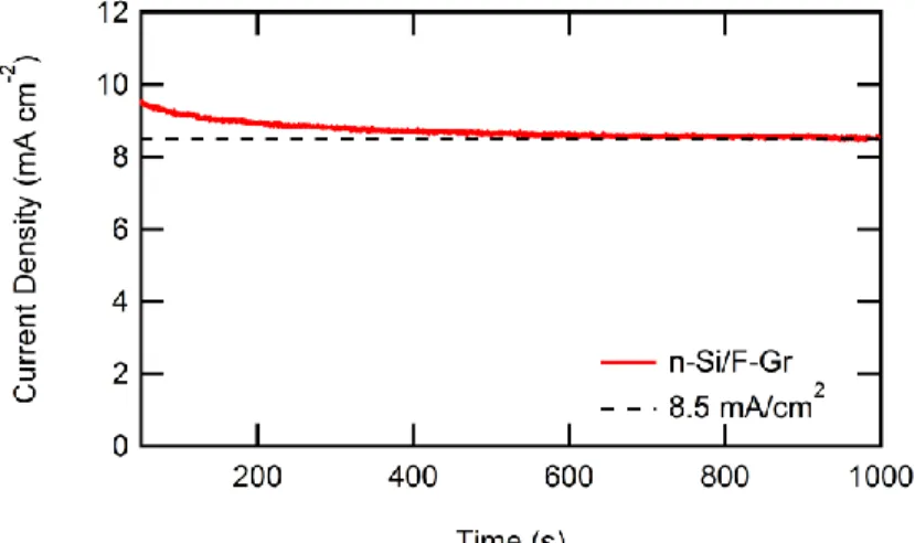
Figure 7. Representative J-t data of an n-Si/F–Gr electrode in contact with aqueous 50 mM Fe(CN)63- - 350 mM Fe(CN)64- under ~33 mW cm-2 of W-halogen illumination.
After an initial decay in current density, the current density stabilized at ~8.5 mA cm-2.
covered (and F–Gr covered) electrodes displayed an initial decay of current density followed by a subsequent stabilization, as seen in Figure 7. This behavior is consistent with the hypothesis that any pinholes in the graphene protective coating led to the oxidation at the exposed Si surface, but that stability is observed when the exposed Si is passivated with SiOx. However, the other batch (batch Gr_C, Figure 8c) yielded only two n-Si/Gr electrodes out of six that exhibited stable current densities for > 1000 s (2/6 stable). The inconsistent behavior in the photoelectrochemical stability imparted by pristine graphene coatings on n-Si electrode was observed over many iterations of graphene growth and electrode fabrication. Conversely, both batches of F–Gr coated n- Si electrodes (batch F–Gr_B, Figure 8b and batch F–Gr_D, Figure 8d) yielded n-Si/F–Gr electrodes that exhibited stable current densities for > 1000 s (5/5 stable in batch F–
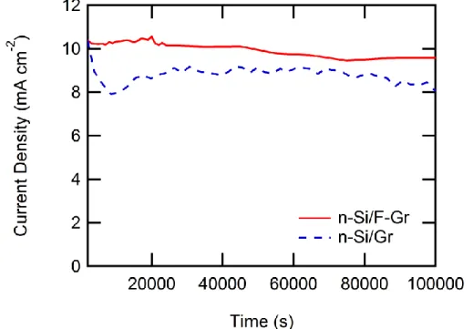
Gr_B and 5/5 stable in batch F–Gr_D). Figure 9 shows the behavior of occasional
‘champion’ electrodes that could be fabricated from Gr or F–Gr with stability over 100,000 s. The improved consistency of the photoelectrochemical stability is one of the key attributes of the fluorinated graphene-coated n-Si electrodes relative to the routinely observed behavior of pristine graphene-coated n-Si electrodes.
Figure 8. J-t data for n-Si/Gr and n-Si/F–Gr electrodes from two different Gr growths in contact with aqueous 50 mM Fe(CN)63- - 350 mM Fe(CN)64- under ~33 mW cm-2 of W-halogen illumination. (A) The n-Si/Gr from the first Gr sheet (growth 1)
exhibited stable current densities for > 1000 s. (B) Fluorination of Gr from growth 1 yielded n-Si/F–Gr electrodes that exhibited stable current densities for > 1000 s. (C) Another Gr growth (growth 2) yielded n-Si/Gr electrodes that did not exhibit stable current densities for > 1000 s. (D) When Batch 2 was fluorinated, the n-Si/F–Gr electrodes exhibited stable current densities for > 1000 s.
Fluorinated graphene-coated and pristine graphene-coated n-Si electrodes were tested for photoelectrochemical stability under approximately 1 sun conditions (~100 mW cm-2 from an ENH-type W-halogen lamp). Figure 10a depicts the photoelectrochemical stability over 1000 s for n-Si/Gr and n-Si/F–Gr electrodes in contact with aqueous 50 mM Fe(CN)63- - 350 mM Fe(CN)64- under ~100 mW cm-2 of W-halogen illumination. The current density of the n-Si/F–Gr electrode was effectively constant over this time period, whereas the current density of the n-Si/Gr electrode decayed from ~25 mA cm-2 to less than 7 mA cm-2 over the same time period. This behavior supports the hypothesis that under these conditions fluorinated graphene provides a superior protective layer relative to pristine graphene. Figure 10b further depicts the photoelectrochemical stability under
Figure 9. J-t data of the ‘champion’ n-Si/F–Gr and n-Si/Gr electrodes in contact with aqueous 50 mM Fe(CN)63- - 350 mM Fe(CN)64- under ~33 mW cm-2 of W- halogen illumination. After both starting at an initial current density of ~10 mA cm-2, the n-Si/F–Gr electrode current density decayed to 9.5 mA cm-2 compared to the n- Si/Gr electrode which decayed to 8 mA cm-2.
the same conditions of a F–Gr coated n-Si electrode over 100,000 s. Although the F–Gr coated electrode was stable over the same time period (100,000 s) under lower light intensity conditions (Figure 3), at near 1 sun conditions the current density of the electrode decayed to near baseline conditions over the same time period.
Figure 10. J-t data for n-Si/Gr and n-Si/F–Gr electrodes in contact with aqueous 50 Mm Fe(CN)63- - 350 mM Fe(CN)64- under ~100 mW cm-2 of W-halogen illumination (A) over 1000 s and (B) a n-Si/F–Gr electrodes under the same conditions over 100,000 s.
Chemical stability
The Raman spectra and optical images of the samples soaked in acidic and neutral solutions showed no change after testing (Figure 11-12). The samples tested in alkaline solutions showed a marked decrease in defect density of the remaining sections of fluorinated graphene, closely mimicking the profile of pristine graphene. Repeated tests of fluorinated graphene in 1 M KOH(aq) showed large-scale delamination of the fluorinated graphene sheet, as observed in the images before and after exposure to the aqueous pH 14 solution.
Figure 11. Stability tests of F–Gr in acidic (1 M HCl), alkaline (1 M KOH), and neutral (deionized water) conditions. An initial Raman of the pristine graphene sheets before fluorination and after fluorination showed an increase in the size of the defect peak at 1350 cm-1. This defect peak remained unchanged after 1 h in acidic or neutral solutions. In contrast, immersion for 1 h in alkaline media produced a decrease in the density of the defect peak.
Figure 12. Optical images of stability tests of F–Gr in acidic (1 M HCl), alkaline (1M KOH), and neutral (deioninzed water) conditions. Arrows indicate points of
reference for the corresponding before and after images.
The chemical stability of the F–Gr to the formation of silicide was also probed. XP spectra of Si-Me/F-Gr/Pt and Si-Me/Pt surfaces were obtained to investigate the ability of F-Gr to inhibit platinum silicide formation (Figure 13). Pt was deposited at ~3 nm thickness via electron-beam evaporation on both F-Gr covered and bare Si surfaces.
The 3 nm Pt thickness was chosen to allow for interrogation of the sample surface to a depth at which both Si and Pt ware observable by XPS. Methylated Si surfaces were used to inhibit the formation of Si oxide at the Si/Pt interface during sample fabrication, because Si oxide of sufficient thickness is also capable of preventing silicide formation.5 Figure 13a shows the XP spectrum of a pure Pt phase. A thicker Pt layer (20 nm) was used to interrogate only the pure Pt phase. Figure 13b shows the Pt 4f XP spectrum of CH3-terminated Si with a 3 nm Pt overlayer. The Pt 4f peak shifted to higher binding energy, indicative of platinum silicide formation.6 The shoulder of the peak at low binding energy is consistent with a pure Pt phase overlayer. Conversely, 3 nm of Pt on F-Gr covered silicon showed essentially no change in the Pt 4f binding energy immediately after fabrication (Figure 13c or after a 1 h anneal under forming gas at 300 °C (Figure 13d)). Figure 13e presents an overlay of the spectra in Figure 13a-13d and highlights the difference between the Pt 4f peak positions. The data are thus indicative of little or no platinum silicide formation.
Figure 13. The Pt 4f XP spectra of Pt on both F-Gr covered and Si
surfaces. (A) XP spectrum of a thick (20 nm) layer of Pt on Si. This spectrum is representative of a pure Pt phase. (B) XP spectrum of a 3 nm layer of Pt on Si. The Pt 4f peak shifted to high binding energy (72.2 and 75.6 eV), characteristic of platinum silicide formation.6 The shoulder to lower binding energy is attributed to a pure Pt phase. (C) XP spectrum of Si-Me/F-Gr/Pt (3 nm).
The Pt 4f peak positions (71.0 and 74.3 eV) are consistent with pure Pt.
(D) XP spectrum of Si-Me/F-Gr/Pt after annealing at 300 °C under forming gas. (E) Overlay of XP spectra (A)-(D).
Figure 14. Electrochemical behavior of n-Si/F–Gr and n-Si–
H electrodes with and without Pt deposition in aqueous 0.4 M Br2
– 7.0 M HBr (pH=0) electrolyte under 33 mW cm-2 from an ELH- type W-halogen lamp). (A) J-E behavior of n-Si/F–Gr and n-Si–
H electrodes with and without Pt deposition. Each cyclic
voltammogram was started at +0.4 V vs. E(A/A-) and swept twice to more negative
potentials at 50 mV s-1. (B) J-t behavior of an n-Si/F–Gr/Pt electrode over 45 minutes at E=0 V vs. E(A/A-) (C) J-E behavior of an n-Si/F–Gr/Pt electrode after exposure to conditions described in (B).
Figure 14 displays the J-E behavior of n-Si–H and n-Si/F–Gr electrodes under
~33 mW cm-2 illumination intensity in contact with 0.4 M Br2 – 7.0 M HBr (pH=0), with and without electrochemical deposition of 100 mC cm-2 of a Pt catalyst, respectively.
With the Pt catalyst, the properties of the n-Si/F–Gr/Pt electrode improved to Voc (n-Si/F–
Gr/Pt) = 0.26 V, ff = 0.52, and Jsc = 8.3 mA/cm2 from Voc (n-Si/F–Gr) = 0.22 V, ff = 0.16, Jsc = 5.14 mA cm -2. The improved ff can be ascribed to improved catalysis for the Br- to Br2 reaction effected by the Pt. The current density of the n-Si–H/Pt electrode under illumination decayed precipitously over two potential sweeps, while the n-Si/F–Gr/Pt electrode showed a stable ff and photocurrent density under the same conditions. The n- Si/F–Gr/Pt electrode had an ideal regenerative cell efficiency (IRC) of 3.5% in contact with the Br2/HBr(aq) electrolyte.33 The current density at n-Si/F-Gr/Pt electrodes was stable over 45 min at E=0 V vs. the Nernstian potential of the solution, E(A/A-) and IRC
increased to 5% over this time (Figure 15). The improvement in IRC indicates a change in the energetics of the n-Si/F–Gr/Pt interface after electrochemical deposition of Pt.
Figure 15. Current density-potential (J-E) behavior of an n-Si/F-Gr/Pt photoanode before, during, and after 2400 s of photoelectrochemical stability testing in contact with 0.4M Br2 - 7.0 M HBr (pH=0) aqueous electrolyte. Photoelectrochemical stability was measured by observing the J-t behavior at an initial current density of 10 mA cm-2 over the specified time period (see Figure 14). The behavior of the n- Si/F-Gr/Pt electrode improved over 2400 s, with improvements in Voc (0.27 V to 0.37 V), JSC (9.0 mA to 9.5 mA), and ff (0.51 to 0.59), resulting in an increase in the ideal regenerative cell conversion efficiency rom 3.5% to >5%.
Assuming 100% faradaic yield for charge transfer to platinum during the photoelectrochemical deposition of Pt from an aqueous solution of 5 mM K2PtCl4 and 200 mM LiCl, in conjunction with 2 e- per Pt atom deposited, and a conformal deposition, a charge density of -100 mC cm-2 should result in the deposition of a ~50 nm thick of Pt layer on the nSi/F–Gr electrodes. SEM images were obtained on n-Si/F–Gr surfaces
Figure 16. SEM of fluorinated graphene before and after photoelectrochemical
deposition of Pt metal from an aqueous solution of 5 mM K2PtCl4 and 200 mM LiCl. A) SEM image of a fluorinated graphene-covered n-Si surface prior to deposition. B) SEM image of a fluorinated graphene-covered n-Si surface after passing 10 mC cm-2 charge during deposition. C) SEM image of a fluorinated graphene-covered n-Si surface after passing 100 mC cm-2 charge during deposition.
before photoelectrochemical deposition and after 10 mC cm-2 or 100 mC cm-2 of cathodic charge density was passed during electrodeposition (Figure 16). Figure 16 indicates that the Pt deposited stochastically across the F–Gr surface. This deposition stands in contrast to previous reports of metal deposition via other methods on graphene, which produced preferential metal deposition at grain boundaries. This difference in behavior may be due to passivation of highly reactive grain boundary sites by the XeF2 treatment.
The incomplete electrochemical stability observed in Figure 14 for the n-SiH/Pt electrode may be related to imperfect conformal deposition, consistent with the observations of Figure 16.
Discussion
A key hypothesis of this work is that the fluorination of CVD-grown graphene leads to passivation of defect sites present in CVD graphene. Assuming a carbon- carbon bond length of 0.142 nm and the hexagonal structure of graphene, the area of each hexagonal unit in a graphene sheet is 0.052 nm2 and encompasses two carbon atoms. Therefore, a 1 cm2 sheet of pristine graphene will include ~ 1x10¹⁵ carbon atoms.
A rigorous evaluation of the density and total number of carbon atoms in a
polycrystalline graphene sheet is challenging, due to the presence of a variety of defect types, including point and line defects, with various geometries, and also due to a
variable number of defects that may be produced by fabrication of the graphene-covered electrode. For simplicity, we consider only the line defects associated with grain
boundaries. These line defects have a variety of geometries and can be composed of alternating 5- and 7- membered carbon rings. Assuming that the density of carbon atoms at a line defect and in the defect-free graphene sheet are equivalent, and further that the density of carbon atoms in a polycrystalline CVD graphene sheet is equivalent to that in a single crystalline graphene sheet, allows calculation of the percentage of total carbon
atoms at defect sites in the graphene sheet. The grain size of the graphene used in this work is 0.2-5 μm on a side. The grains are generally amorphously shaped, but are approximated herein as hexagons for simplicity. Assuming hexagonal grains with side length of 0.2 μm (area of 0.10 μm2) implies ~109 grains in a 1 cm2 sheet of graphene, and a total length of 8 x 108 μm of grain boundary area. If the width of these boundaries is equal to the width of a single hexagonal unit of the graphene lattice (~0.28 nm), and assuming that the carbon density is the same as that of a single hexagonal unit, the total number of defect carbon atoms at grain boundary line defects is ~1010C atoms per 1 cm2 area of graphene. Thus (1010 /1015), i.e., 1 defective carbon atom is present for every 105 pristine carbon atoms in the polycrystalline graphene sheet. This ratio is significantly smaller than the ratio of F atoms to C atoms found via XPS analysis (10 > F/C > 0.01). In conjunction with the expectation that the defect sites on a graphene sheet are
significantly more reactive than the pristine carbon sites, this XPS F/C ratio suggests that most or all of the defect carbon atoms are capped with fluorine.
Prior to the stability test, the open-circuit potential (Voc) of the n-Si/F–Gr electrode was -0.27 V vs. E(A/A-), approximately 70 mV lower than the reported VOC of -0.34 V vs.
E(A/A-) for n-Si coated with a single layer of graphene.22 Further, exposure of n-Si/F-Gr to a series of non-aqueous electrolytes of varying electrochemical potential showed a dependence of Voc on E(A/A-), indicating partial Fermi level pinning of the n-Si surface with respect to the solution potential (Table 1). The mutually similar fill factors (ff) the n- Si/F–Gr electrode and np+-Si/F–Gr electrodes, 0.33 and 0.30, respectively (Figure 3c, Figure 4c), indicated similar limiting resistance to charge transfer in both systems.
Additional tests of the chemical stability demonstrate that F-Gr is also an effective barrier against other deleterious surface reactions. F-Gr covered Si surfaces did not form platinum silicide upon evaporation of Pt onto the F–Gr/Si surface, and F–Gr is stable in both aqueous and acidic (pH 0) solutions, suggesting F–Gr also provides an
effective physical barrier to inhibit Pt/Si reactivity and is stable under harsh fabrication and electrolyte conditions. Although only lightly fluorinated (CxF, x > 10) graphene was used herein, these fluorinated graphene sheets provided superior protection against corrosion to the underlying Si relative to the protection imparted by monolayer graphene on n-Si(111) photoanodes (Figure 8).22 These results are consistent with the hypothesis that light fluorination of graphene induces reaction with high-energy defect sites, such as dangling bonds or missing atoms, effectively sealing defects that otherwise would allow oxide formation at the n-Si surface and further degradation of the Gr protective layer.
The bonding of a very electronegative atom to the surface may also increase the hydrophobicity of the graphene sheet, which would further reduce deleterious corrosion reactions near pinholes.
Conclusion
Fluorinated graphene forms an effective physical barrier between silicon surfaces and a number of contacting phases, including acidic and neutral pH aqueous electrolyte as well as metallic interfaces. Additionally, Si covered by fluorinated graphene exhibits partial Fermi level pinning in contact with non-aqueous electrolytes. Additional work at higher fluorination levels on both p-type and n-type silicon will elucidate whether a reduction in the density of states near the Fermi level can lead to a fully unpinned
interface, and will allow elucidation of the effect of the graphene-based surface dipole on the electrochemical behavior of the resultant photoelectrode.
References
1. Hu, S.; Lewis, N. S.; Ager, J. W.; Yang, J.; McKone, J. R.; Strandwitz, N. C., Thin-Film Materials for the Protection of Semiconducting Photoelectrodes in Solar-Fuel Generators. J. Phys. Chem. C 2015, 119 (43), 24201-24228.
2. Sun,
K.; Shen, S.; Liang, Y.; Burrows, P. E.; Mao, S. S.; Wang, D., Enabling Silicon for Solar- Fuel Production. Chem. Rev. 2014, 114 (17), 8662-8719.
3. Sun, K.; McDowell, M. T.; Nielander, A. C.; Hu, S.; Shaner, M. R.; Yang, F.;
Brunschwig, B. S.; Lewis, N. S., Stable Solar-Driven Water Oxidation to O2(g) by Ni- Oxide-Coated Silicon Photoanodes. J. Phys. Chem. Lett. 2015, 6 (4), 592-598.
4. Hu, S.; Shaner, M. R.; Beardslee, J. A.; Lichterman, M.; Brunschwig, B. S.;
Lewis, N. S., Amorphous TiO2 coatings stabilize Si, GaAs, and GaP photoanodes for efficient water oxidation. Science 2014, 344 (6187), 1005-1009.
5. Strandwitz, N. C.; Comstock, D. J.; Grimm, R. L.; Nichols-Nielander, A. C.; Elam, J.; Lewis, N. S., Photoelectrochemical Behavior of n-type Si(100) Electrodes Coated with Thin Films of Manganese Oxide Grown by Atomic Layer Deposition. J. Phys. Chem. C 2013, 117 (10), 4931-4936.
6. Bélanger, D.; Dodelet, J. P.; Lombos, B. A., Characteristics and Stability of n ‐ Si / SnO2 and n ‐ Si / SnO2 / Pt Photoanodes. J. Electrochem. Soc. 1986, 133 (6), 1113- 1119.
7. Contractor, A. Q.; Bockris, J. O. M., Investigation of a protective conducting silica film on n-silicon. Electrochim. Acta 1984, 29 (10), 1427-1434.
8. Howe, A. T.; Hawkins, R. T.; Fleisch, T. H., Photoelectrochemical Cells of the Electrolyte‐Metal‐Insulator‐Semiconductor (EMIS) Configuration: I . Metal Thickness and
Coverage Effects in the Pt/Silicon Oxide/n‐Si System. J. Electrochem. Soc. 1986, 133 (7), 1369-1375.
9. Menezes, S.; Heller, A.; Miller, B., Metal Filmed‐Semiconductor Photoelectrochemical Cells. J. Electrochem. Soc. 1980, 127 (6), 1268-1273.
10. Sze, S. M.; Ng, K., K., Physics of Semiconductor Devices. 3rd ed.; John Wiley &
Sons, Inc.: Hoboken, NJ, 2007.
11. Chen, Y. W.; Prange, J. D.; Dühnen, S.; Park, Y.; Gunji, M.; Chidsey, C. E. D.;
McIntyre, P. C., Atomic layer-deposited tunnel oxide stabilizes silicon photoanodes for water oxidation. Nat. Mater. 2011, 10 (7), 539-544.
12. Fonash, S. J., Solar Cell Device Physics. 2nd ed.; Elsevier Inc.: Amsterdam, 2010.
13. Bansal, A.; Lewis, N. S., Stabilization of Si Photoanodes in Aqueous Electrolytes through Surface Alkylation. J. Phys. Chem. B 1998, 102 (21), 4058-4060.
14. Bansal, A.; Lewis, N. S., Electrochemical Properties of (111)-Oriented n-Si Surfaces Derivatized with Covalently- Attached Alkyl Chains. J. Phys. Chem. B 1998, 102 (7), 1067-1070.
15. Bolts, J. M.; Bocarsly, A. B.; Palazzotto, M. C.; Walton, E. G.; Lewis, N. S.;
Wrighton, M. S., Chemically derivatized n-type silicon photoelectrodes. Stabilization to surface corrosion in aqueous electrolyte solutions and mediation of oxidation reactions by surface-attached electroactive ferrocene reagents. J. Am. Chem. Soc. 1979, 101 (6), 1378-1385.
16. Chen, S.; Brown, L.; Levendorf, M.; Cai, W.; Ju, S.-Y.; Edgeworth, J.; Li, X.;
Magnuson, C. W.; Velamakanni, A.; Piner, R. D.; Kang, J.; Park, J.; Ruoff, R. S., Oxidation Resistance of Graphene-Coated Cu and Cu/Ni Alloy. ACS Nano 2011, 5 (2), 1321-1327.
17. Flynn, G. W., Perspective: The dawning of the age of graphene. J. Chem. Phys.
2011, 135 (5), 050901-8.
18. Lee, Y.; Bae, S.; Jang, H.; Jang, S.; Zhu, S.-E.; Sim, S. H.; Song, Y. I.; Hong, B.
H.; Ahn, J.-H., Wafer-Scale Synthesis and Transfer of Graphene Films. Nano Lett. 2010, 10 (2), 490-493.
19. Prasai, D.; Tuberquia, J. C.; Harl, R. R.; Jennings, G. K.; Bolotin, K. I., Graphene:
Corrosion-Inhibiting Coating. ACS Nano 2012, 6 (2), 1102-1108.
20. Suk, J. W.; Kitt, A.; Magnuson, C. W.; Hao, Y.; Ahmed, S.; An, J.; Swan, A. K.;
Goldberg, B. B.; Ruoff, R. S., Transfer of CVD-Grown Monolayer Graphene onto Arbitrary Substrates. ACS Nano 2011, 5 (9), 6916-6924.
21. Sutter, E.; Albrecht, P.; Camino, F. E.; Sutter, P., Monolayer graphene as ultimate chemical passivation layer for arbitrarily shaped metal surfaces. Carbon 2010, 48 (15), 4414-4420.
22. Nielander, A. C.; Bierman, M. J.; Petrone, N.; Strandwitz, N. C.; Ardo, S.; Yang, F.; Hone, J.; Lewis, N. S., Photoelectrochemical Behavior of n-Type Si(111) Electrodes Coated With a Single Layer of Graphene. J. Am. Chem. Soc. 2013, 135 (46), 17246- 17249.
23. Droscher, S.; Roulleau, P.; Molitor, F.; Studerus, P.; Stampfer, C.; Ensslin, K.;
Ihn, T., Quantum capacitance and density of states of graphene. Appl. Phys. Lett. 2010, 96 (15), 152104-3.
24. Ponomarenko, L. A.; Yang, R.; Gorbachev, R. V.; Blake, P.; Mayorov, A. S.;
Novoselov, K. S.; Katsnelson, M. I.; Geim, A. K., Density of States and Zero Landau Level Probed through Capacitance of Graphene. Phys. Rev. Lett. 2010, 105 (13), 136801.
25. Bae, S.; Kim, H.; Lee, Y.; Xu, X.; Park, J.-S.; Zheng, Y.; Balakrishnan, J.; Lei, T.;
Ri Kim, H.; Song, Y. I.; Kim, Y.-J.; Kim, K. S.; Ozyilmaz, B.; Ahn, J.-H.; Hong, B. H.;
Iijima, S., Roll-to-roll production of 30-inch graphene films for transparent electrodes.
Nat. Nano. 2010, 5 (8), 574-578.
26. Nair, R. R.; Ren, W.; Jalil, R.; Riaz, I.; Kravets, V. G.; Britnell, L.; Blake, P.;
Schedin, F.; Mayorov, A. S.; Yuan, S.; Katsnelson, M. I.; Cheng, H.-M.; Strupinski, W.;
Bulusheva, L. G.; Okotrub, A. V.; Grigorieva, I. V.; Grigorenko, A. N.; Novoselov, K. S.;
Geim, A. K., Fluorographene: A Two-Dimensional Counterpart of Teflon. Small 2010, 6 (24), 2877-2884.
27. Robinson, J. T.; Burgess, J. S.; Junkermeier, C. E.; Badescu, S. C.; Reinecke, T.
L.; Perkins, F. K.; Zalalutdniov, M. K.; Baldwin, J. W.; Culbertson, J. C.; Sheehan, P. E.;
Snow, E. S., Properties of fluorinated graphene films. Nano Lett. 2010, 10 (8), 3001-5.
28. Stine, R.; Lee, W.-K.; Whitener, K. E.; Robinson, J. T.; Sheehan, P. E., Chemical Stability of Graphene Fluoride Produced by Exposure to XeF2. Nano Lett. 2013, 13 (9), 4311-4316.
29. Petrone, N.; Dean, C. R.; Meric, I.; van der Zande, A. M.; Huang, P. Y.; Wang, L.;
Muller, D.; Shepard, K. L.; Hone, J., Chemical Vapor Deposition-Derived Graphene with Electrical Performance of Exfoliated Graphene. Nano Lett. 2012, 12 (6), 2751-2756.
30. Pirkle, A.; Chan, J.; Venugopal, A.; Hinojos, D.; Magnuson, C. W.; McDonnell, S.;
Colombo, L.; Vogel, E. M.; Ruoff, R. S.; Wallace, R. M., The effect of chemical residues on the physical and electrical properties of chemical vapor deposited graphene
transferred to SiO2. Appl. Phys. Lett. 2011, 99 (12), -.
31. Plymale, N. T.; Kim, Y.-G.; Soriaga, M. P.; Brunschwig, B. S.; Lewis, N. S., Synthesis, Characterization, and Reactivity of Ethynyl- and Propynyl-Terminated Si(111) Surfaces. J. Phys. Chem. C 2015, 119 (34), 19847-19862.
32. Hao, Y.; Bharathi, M. S.; Wang, L.; Liu, Y.; Chen, H.; Nie, S.; Wang, X.; Chou, H.;
Tan, C.; Fallahazad, B.; Ramanarayan, H.; Magnuson, C. W.; Tutuc, E.; Yakobson, B. I.;
McCarty, K. F.; Zhang, Y.-W.; Kim, P.; Hone, J.; Colombo, L.; Ruoff, R. S., The Role of
Surface Oxygen in the Growth of Large Single-Crystal Graphene on Copper. Science 2013, 342 (6159), 720-723.
33. Coridan, R. H.; Nielander, A. C.; Francis, S. A.; McDowell, M. T.; Dix, V.;
Chatman, S. M.; Lewis, N. S., Methods for comparing the performance of energy- conversion systems for use in solar fuels and solar electricity generation. Energy Environ. Sci. 2015, 8 (10), 2886-2901.