Compound Meta-optics for Complete Wavefront Control
By Hanyu Zheng
Dissertation
Submitted to the Faculty of the Graduate School of Vanderbilt University
in partial fulfillment of the requirements for the degree of
DOCTOR OF PHILOSOPHY in
Electrical Engineering May 12, 2023 Nashville, Tennessee
Approved:
Jason G. Valentine, Ph.D.
Joshua Caldwell, Ph.D.
Sharon M. Weiss, Ph.D.
Justus Ndukaife, Ph.D.
Yuankai Huo, Ph.D.
ii
Copyright © 2023 by Hanyu Zheng All Rights Reserved
iii DEDICATION
To my beloved mom and dad.
iv
ACKNOWLEDGEMENTS
Vanderbilt University has been a special place for me in the past five years when I pursued a Ph.D. in electrical engineering. I would like to express my heartfelt gratitude to this place for providing me with an exceptional educational experience. The resources and opportunities available at this prestigious campus have significantly impacted my current achievements and shaped me into the present person. This fantastic platform also offers me a balanced work-life environment so that I can conduct my research readily.
I would like to thank my Ph.D. advisor, Dr. Jason Valentine, one of the most intelligent scientists I have ever met, who offered me the opportunity to research at Vanderbilt. During my Ph.D. career, Dr. Valentine inspired me a lot, not only in conducting hands-on experiments but also the critical thinking to be an independent investigator. Through weekly discussions with Dr.
Valentine, I developed solid research skills and visionary ideas so that we can always conduct projects at the frontiers of metasurface realms. Besides, Dr. Valentine is also extremely helpful to my academic career and supports me in attending major conferences to build networks with peers.
I learned a lot from his scientific skills and personality that shaped me into the person I would like to be as an academic researcher.
I would also like to thank Dr. Jousha Caldwell, Dr. Sharon Weiss, Dr. Justus Ndukaife, and Dr. Yuankai Huo, who served as my committee members and supported me during my research projects. Thanks to their helpful feedback, my Ph.D. dissertation has become more solid and comprehensive. I benefited greatly through communications with them over the past five years.
From the classes of Dr. Weiss and Dr. Ndukaife, I built up the fundamentals of photonics, which assisted me in further understanding my research projects. I also learned a lot from collaborating with Dr. Caldwell and Dr. Huo, as we proposed many frontiered research projects together.
v
I want to thank our research collaborators, Dr. Anthony Grbic and Dr. Brian O. Raeker from Michigan University. Thanks for your diligent effort in the compound meta-optic research.
The collaboration inspired me a lot so that I could build basic concepts and experimental skills around compound meta-optic devices. I also want to thank Mingze He and Quan Liu from Vanderbilt University, who shared plenty of ideas from the computer science aspects so that we could readily develop the optimization platform.
Besides, I would like to thank my labmates in Dr. Valentine’s group. Your optimism toward research and life encourages me a lot so that I can enjoy my Ph.D. career. Specifically, I want to thank You Zhou, a visionary and intelligent person mentoring me at the beginning of my Ph.D. who can always generate great ideas during our discussions. I also want to thank Chibuzor Fabian Ugwu, Elena Kovalik, Janna Eaves, Scott Criswell, Brandon Swartz, Andrew Du, and Xiaomeng Zhang. I learned a lot while working with you, not only in research but also in our friendly communications about daily life. I want to offer special thanks to Tao Hong, who taught me solid fishing skills. Hope you can catch the dream fish very soon.
Moreover, I want to thank the staff in the VINSE family. I want to thank Kurt Heinrich, William Martinez, Alice Leach, Benjamin W. Schmidt, Christina L. McGahan, James R. McBride, Dmitry S. Koktysh, and Megan K. Dernberger. Thank you for your strong technical support during my research so I could finish my experiments smoothly. I also want to thank Sarah Ross, Jamie L.
Kuntz, Daniel Myrtles, and Cassidy Slabaugh for their exceptional administrative support, including filling out the purchase order and scheduling the events.
Lastly, I want to thank my family members, my mon, my dad, my girlfriend Lexi, and my kittens, Iri and Luna. Thank you for your tolerance and patience with me. I cannot finish my Ph.D.
without your support. You are the most valuable treasure in my life.
vi
TABLE OF CONTENTS
DEDICATION ... iii
ACKNOWLEDGEMENTS ... iv
LIST OF TABLES ... viii
LIST OF FIGURES ... ix
LIST OF ABBREVIATIONS ... xvii
LIST OF PUBLICATIONS ... xx
Chapter 1. Introduction ... 1
1.1 Origins of Metasurfaces ... 1
1.2 Dielectric Metasurfaces for Wavefront Engineering ... 3
1.3 Design Strategy of Metasurfaces ... 5
1.4 Meta-optic-based Applications ... 7
1.5 Compound Meta-optic Systems ... 10
1.6 Organization of the Thesis ... 12
2. Compound Meta-optics for Field Control ... 15
2.1 Introduction ... 15
2.2 Design Strategy of Phase-only Compound Meta-optics ... 18
2.3 Compound Meta-optics for Lossless and Complex-valued Field Control ... 21
2.4 Physics Driven End-to-end Optimization for Compound Meta-optics ... 29
2.5 Compound Meta-optics for Lossless and Complete Field Control ... 33
2.6 Conclusion ... 40
3. Meta-optic Accelerators for Object Classifiers ... 42
3.1 Introduction ... 42
3.2 Meta-optic Accelerators for Convolutional Neural Network ... 45
3.3 Meta-optic Accelerators for Multifunctional Classification ... 55
3.4 Complex-amplitude Manipulation for Object Classifier ... 57
3.5 Comparison between Hybrid and Diffractive Neural Networks ... 59
3.6 Further Optimization for Optical Frontend ... 61
3.7 Conclusion ... 64
4. Nanosphere Lithography based Large-scale Metasurfaces ... 65
4.1 Introduction ... 65
vii
4.2 Nanosphere Self-assembly Method ... 66
4.3 Image Processing based on Large-scale Compound Meta-optic ... 68
4.4 Non-periodic Large-scale Metasurface Manufacture and Applications ... 74
4.5 Robustness Analysis of Nanosphere Lithography ... 81
4.6 Conclusion ... 87
5. Conclusion and Outlook ... 88
5.1 Summary ... 88
5.2 Prospects ... 90
Appendix A. Fundamentals of Metasurfaces ... 94
A.1 Sampling Rule for Metasurfaces ... 94
A.2 Jones Calculus for Birefringent Metasurfaces ... 94
A.3 Refractive Index of Silicon ... 95
A.4 Angular Spectrum Propagation Method ... 96
B. Compound Meta-optics for Field Control ... 99
B.1 Gerchberg-Saxton Algorithm ... 99
B.2 In-situ Alignment System for Compound Meta-optics ... 100
B.3 Methods for Birefringent and Complex-valued Field Control ... 102
B.4 Role of k-space Filter in the End-to-end Optimization Platform ... 104
B.5 Target Fields of Meta-optics for Complete Field Control ... 104
B.6 Arbitrary Mode Conversion Using Compound Meta-optics ... 106
C. Meta-optic Accelerators for Object Classifiers ... 109
C.1 Meta-atoms for Meta-optic Accelerators ... 109
C.2 Optical Characterization Setup for Meta-optic Accelerators ... 110
C.3 Meta-optic Accelerators for Complex Signal Recognition ... 111
D. Nanosphere Lithography based Large-scale Metasurfaces ... 113
D.1 Nanosphere Lithography Procedure ... 113
D.2 Optical Characterization Setup for Large-scale Metasurfaces ... 114
REFERENCES ... 116
viii
LIST OF TABLES
Table Page Table 2.1 Manipulation parameters of each image component to assemble the 3-dimensional hologram ... 25 Table 3.1 FLOPs of proposed neural network architecture ... 53
ix
LIST OF FIGURES
Figure Page
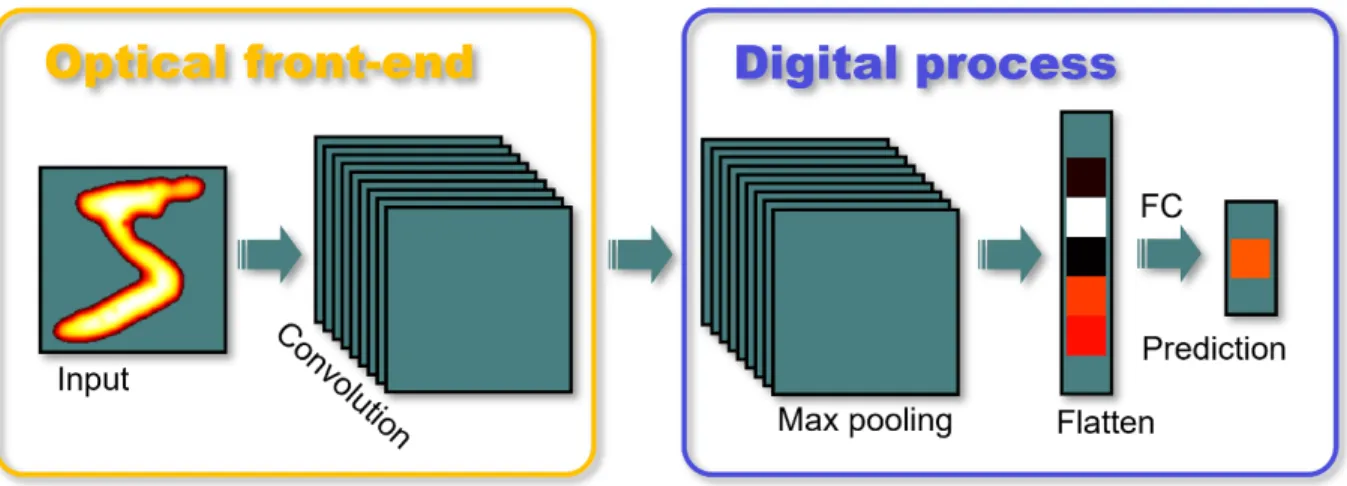
Figure 1.1 Schematics of photonic feature size and interacting wavelength. The hexagram means artificially fabricated unit cells. ... 1 Figure 1.2 Mechanism of metasurface for wavefront control. (a) Schematics of generalized Snell’s law. (b) Light control by each unit cell in metasurfaces for anomalous refraction. ... 2 Figure 1.3 Electrical field map of periodic metasurfaces for phase manipulation. The simulated wavefront shows different phase responses under plane-wave illumination dictated by the diameters of silicon-based nanopillars. The period is fixed at 0.5𝜆, Height is 0.7𝜆 and diameter is controlled at (a) 0.08𝜆, (b) 0.16𝜆 and (c) 0.24𝜆, respectively. All metasurfaces are embraced in a polymer surrounding environment with an index of 1.48. ... 4 Figure 1.4 Electrical field map of metasurfaces for anomalous refraction. (a) The schematic of a period of metasurface for anomalous refraction. The period includes six different meta-atoms.
Each is independent and chosen from a prior data library with designed phase responses as labeled.
(b) A full wave simulation based on the structure in (a) indicates an anomalous refraction behavior under plane-wave illumination. ... 7 Figure 1.5 Demonstration of birefringent property of cylindroid meta-atom. (a) The geometrical schematic of meta-atom. The period is fixed at 0.5𝜆, Height is 0.7𝜆, diameters are chosen at 0.13𝜆 and 0.32𝜆, respectively. The rotation angle 𝜃 is set at 45°. All metasurfaces are embraced in a polymer surrounding environment with an index of 1.48. (b) and (c) exhibit 𝑥 and 𝑦 polarized electrical field map, indicating a complete polarization conversion process. ... 10 Figure 1.6 Various applications and novel fabrication methods for meta-optics. (a) Compound meta-optics for 3-dimensional displaying. (b) Compound meta-optics for lossless and complete field control. (c) Compound meta-optic as an accelerator for information processing. (d) Meta-optic as an angular filter for edge signal enhancement. (e) Nanosphere-assisted grayscale lithography for large-scale metasurface fabrication. ... 13 Figure 2.1 Complex-field control with metasurfaces. (a) A single metasurface, in the absence of a supercell, enables full and independent control (phase, amplitude, polarization) over one input polarization state. LP stands for linear polarized. (b) The use of supercells enables interference to be used for independent control over unpolarized light but results in loss to higher diffraction orders. UP stands for unpolarized. (c) Bi-layer meta-optics can be used for nearly loss-less full field control for unpolarized light. ... 16 Figure 2.2 The optical compound meta-optic implementing independent phase and amplitude control over an incident optical field. (a) Illustration of a compound meta-optic converting a uniform illumination into a three-dimensional, complex-valued hologram. The depth of the three-dimensional hologram is visualized when the output field is imaged at different depths by an observer facing the device. (b) The transmission characteristics of the unit cell under
x
normally incident plane wave illumination and periodic boundary conditions. The inset shows a schematic of the metasurface unit cell. Each cell has a period of P=570nm and contains an amorphous silicon nanopillar with a height of H=850nm. The nanopillar diameter is varied across the metasurface to implement the desired transmission phase profile. All the silicon nanopillars were embraced by PDMS as the support for the compound metasurface system. ... 18 Figure 2.3 Gerchberg-Saxton algorithm-based design framework to generate a compound metasurface system for complex-amplitude control. 𝐸0 represents the desired complex- amplitude distribution at the target image plane. 𝐸1 is the field distribution at the second metasurface layer. 𝜙𝑀𝑆1 and 𝜙𝑀𝑆2 are the retrieved phase distribution for each metasurface layer to achieve independent amplitude and phase manipulation. ... 19 Figure 2.4 Measurement results of meta-optics implementing a beamforming and splitting function. Uniform circular illumination is manipulated to form multiple Gaussian beams at the output. (a) The phase profile of compound metasurfaces for two Gaussian beams former. (b) and (c) The simulation and measurement results of the output intensity from two Gaussian beams former at the second layer metasurface (left) and far-field (right). (d) The phase profile of compound metasurfaces for three Gaussian beams former. (e) and (f) The simulation and measurement results of the output intensity from three Gaussian beams former at the second layer metasurface (left) and far-field (right). The intensity redistribution and beam splitting indicate well complex-amplitude control. ... 22 Figure 2.5 Measurement results of meta-optics implementing a 3-dimensional hologram. A uniform plane-wave-like illumination was used. The intensity has been normalized to respective maximums. (a) The diagram of the compound meta-optic structure architecture forms the 3d holograms at variant depths. (b) The phase profile of the first(left) and second(right) layer metasurface. (c) The simulated output field intensity profile from the compound meta-optic. The output field was calculated at a variant distance from the second layer metasurface. The bottom- right corner label indicates the distance. (d) The measured output field intensity profile from the compound meta-optic. As a comparison, the distance between the second metasurface and the simulated field was chosen to match the measurement results. ... 26 Figure 2.6 Single-layer phase-only metasurface to produce the 3d hologram. (a) The phase profile of single layer metasurface for hologram generation. (b) The simulated output field intensity from the metasurface. The field was calculated at a variant distance to show a 3d hologram profile. The bottom-right corner label indicates the distance between the hologram and metasurface. ... 28 Figure 2.7 Inverse design of multi-layer meta-optics. (a) Schematic of the birefringent meta- atom. (b) and (c) Transmission coefficient (amplitude and phase) map of the meta-atom under x and y polarized illumination, respectively, as a function of the geometry (width and length). In these maps, the rotation angle of the meta-atom was fixed at 0°. (d) The inverse design architecture allows for optimization of the amplitude, phase, and polarization state. Multiple optimization targets with various propagation distances, indicated by the coordinate (d2, d3, d4), were sampled for robustness. (e) The error function and efficiency of the meta-optic as a function of epoch. .. 30
xi
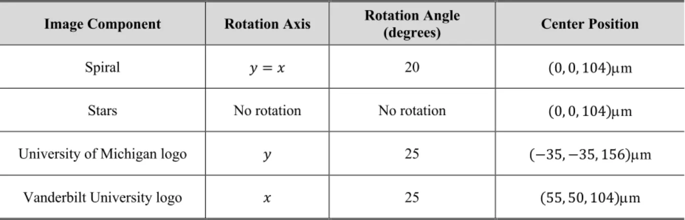
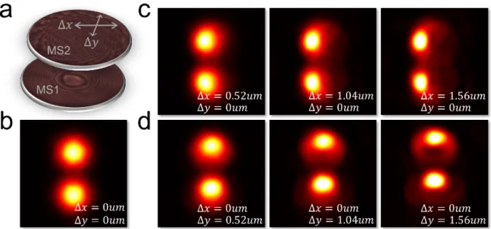
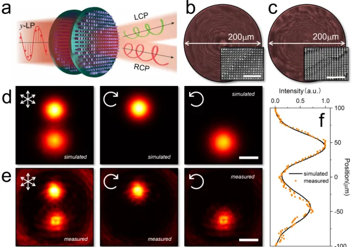
Figure 2.8 Meta-optic-based SDM to unpolarized light. (a) Schematic of the multi-layer meta- optic for SDM to unpolarized beams. (b) and (c) Optical images of each metasurface in the meta- optic. The insets are SEM images of metasurfaces. Scale bar: 4µm. (d) and (e) Simulated and measured polarization-dependent intensity distributions after the meta-optic. An unpolarized supercontinuum laser was used as the source. The arrows in the upper-left corner indicate the analyzer direction, which is unpolarized (left), x-polarized (middle), and y-polarized (right). Scale bar: 50µm. (f) Simulated and measured mode profile after the meta-optic as a function of lateral position. The intensity has been normalized to the maximum value. ... 34 Figure 2.9 Simulated sensitivity to lateral misalignment. (a) Diagram of lateral misalignment.
(b) The simulated output field without any misalignment. (c) and (d) The simulated output field with various misalignment values along the x and y-axis. ... 36 Figure 2.10 Simulated sensitivity to vertical misalignment. (a) Diagram of vertical misalignment. (b) The simulated output field without any misalignment. (c) and (d) The simulated output field with various misalignments values along z-axis. ... 36 Figure 2.11 Meta-optic-based mode conversion for circularly polarized light. (a) Schematic of the multi-layer meta-optic for mode conversion to linearly polarized beams. (b) and (c) Optical images of each metasurface in the meta-optic. The insets are SEM images of metasurfaces. Scale bar: 4µm. (d) and (e) Simulated and measured polarization-dependent intensity distributions after the meta-optic. An unpolarized supercontinuum laser was used as the source. The upper-left corner arrows indicate the analyzer orientation, which is unpolarized (left), LCP (middle), and RCP (right). Scale bar: 50µm. (f) Simulated and measured mode profile after the meta-optic as a function of lateral position. The intensity has been normalized to the maximum value. ... 37 Figure 2.12 Meta-optic-based vectorial hologram. (a) Schematic of the multi-layer meta-optic for the vectorial hologram to unpolarized beams. (b) and (c) Optical images of each metasurface in the meta-optic. The insets are SEM images of metasurfaces. Scale bar: 4µm. (d) and (e) Simulated and measured polarization-dependent intensity distributions after the meta-optic. An unpolarized supercontinuum laser was used as the source. The upper-left corner arrows indicate the analyzer orientation. From left to right, the analyzer state is unpolarized, 15°, 45°, and 75°
polarized to the x-axis. Scale bar: 50µm. ... 39 Figure 3.1 The Schematic of a convolutional neural network. The optical front-end performed object capturing as well as convolution process based on the optical operations. ... 43 Figure 3.2 Schematic of the meta-optic accelerator. The meta-optic enables multi-channel signal processing for replacing convolution operations in a digital neural network. Summing is achieved by each kernel being recorded by a single pixel on the photodetector. ... 44 Figure 3.3 Components of the meta-optic system. (a) The phase profile of the multi-channel metalens was achieved using spatially multiplexed meta-atoms. (b) Optical image of the fabricated multi-channel metalens. The inset is an SEM image of the lens. Scale bar: 2µm. (c) Experimental focal spot profile of the multi-channel metalens under illumination at a wavelength of 1.3µm. (d) Polarization conversion efficiency as a function of the meta-atom rotation angle. (e) Optical image of kernel resolution test chart. The left-side bar shows the number of meta-atoms in each kernel
xii
pixel. Inset is an SEM image of the meta-atoms. Left scale bar: 30µm. Right scale bar: 4µm. (f) Optical transmission of the kernel resolution test char under tungsten lamp illumination. An orthogonal analyzer was used to image the transmission map. Scale bar: 30µm. ... 45 Figure 3.4 Characterization of metasurface-based kernel resolution. (a) The field profile of the test kernel. The white lines indicate the extracted data in (b). The data were extracted according to different meta-atoms numbers in each kernel element. (b) The quantitative description of kernels as a function of meta-atoms number is each kernel element. The top labels indicate the meta-atoms arrangements in a single kernel pixel. ... 48 Figure 3.5 Workflow of the meta-optic accelerator design and testing process. (a) The metalens, with 9 independent channels, splits the image. In training, these images are recorded on the camera and used for training the optical kernel layer and digital systems. Once the kernel layer is trained, it is inserted into the system, and the images are then projected onto that layer generating 9 feature maps that are recorded on the camera (b) The digital loop comprises an iterative training process in which the Jones matrix is used for forward propagation. (c) The probability histogram is the final output for image classification. ... 49 Figure 3.6 Comparison between conventional and optical neural networks. (a) and (b) The weight evolution for conventional and optical neural networks, respectively. (c) The loss evolution for conventional and optical neural networks as a function of training epochs. ... 50 Figure 3.7 The digital neural network architecture used in the manuscript. (a) The neural network for amplitude-only object recognition. (b) The neural network process for polarized object classification. The label above indicates the input neuron numbers of each layer. (c) The size and stride number of kernel for convolution. ... 52 Figure 3.8 Classification of MNIST digits. (a) Transmission (weights) of the ideal kernels after the training process. (b) Measured transmission of the fabricated channels. An incoherent light source, filtered at 1.3µm, was used for illumination. (c) The nine feature maps were recorded on the camera. (d) and (e) is the theoretical and measured confusion matrices for MNIST object classification, respectively. (f) The acceleration by optical convolution in neural networks as a function of input image resolution. The state-of-the-art camera baseline indicates the image recording speed by Phantom TMX 7510. ... 54 Figure 3.9 Demonstration of multi-functional object classification. (a) and (b) illustrate the digits for classification, which carry both amplitude and polarization information. (c) and (d) is the transmission profiles of the fabricated metasurface channels under incoherent, 1.3µm wavelength, illumination with orthogonal linear polarization states. (e) and (f) are feature maps for identical digits with x and y-polarization, respectively. (g) and (h) are the theoretical and measured confusion matrices, respectively. ... 56 Figure 3.10 The complex-amplitude manipulation method for multi-channel metalens. (a) The design process for multi-channel metalens with arbitrary information channels. (b) The schematics of metasurface profiles to construct the complex-amplitude profile in (a). Scale bar:
5µm. (c) The reconstructed complex-amplitude profile based on calculated meta-atoms data library.
xiii
Scale bar: 50µm. (d) The calculated focal spot profile of the multi-channel metalens based on complex-amplitude values in (c). Scale bar: 50µm. ... 58 Figure 3.11 Bandwidth verification of meta-optic system and comparison to diffractive neural networks. (a) A schematic of hybrid neural network. (b) The Strehl of the imaging system in terms of the illumination bandwidth. Insets show point spread function (PSF) of the imaging system in terms of illumination bandwidth. (c) A schematic of a simple diffractive neural network.
(d) The performance of diffractive layer as a function of input aperture size. ... 59 Figure 3.12 Complex-amplitude manipulation method for low stride number convolution.
(a) The digital convolution process with a designed kernel. (b) The designed complex-amplitude profile to operate optical convolution. (c) The convolution process performed by optical operations.
All data in (c) was optical measured based on fabricated devices. (d) The FLOPS of convolution as the function of stride number as well as the input image resolution. ... 63 Figure 4.1 Schematics of nanosphere self-assembly process. (a) The liquid-air interface nanosphere self-assembly setup. (b) SEM image of self-assembled nanosphere array. Inset shows the optical image of the corresponding sample. ... 67 Figure 4.2 The diagram of edge detection based on non-local metasurface. (a) Edge detection process where metasurface serves as a k-space filter. (b) and (c) Image signal intensity distribution in real space (left) and k-space (right). (b) indicates a solid area signal from the pattern, while (c) exhibits the edge signal. The intensities have been normalized to respective maximums. ... 69 Figure 4.3 Simulated optical response of non-local metasurface. (a) and (b) The TE and TM modes based transmitted optical response of metasurface in terms of incident angle and wavelength.
Inset shows the schematic of optical metasurface. (c) The transmittance and phase response of non-local metasurface as a function of incident angle. Dash line represents TE mode while solid line shows the TM mode response. For TM mode, the transmittance line indicates a high-k filter.
... 70 Figure 4.4 Fabrication of large-scale non-local metasurface. (a) The fabrication process based on nanosphere self-assembly technique. (b) The optical image of self-assembled nanosphere array.
The diffracted color indicates various polycrystalline domains in the sample. (c) and (d) The SEM of fabricated non-local metasurface under tilted (c) and top-down (d) perspective. Scale bar: 1µm.
... 72 Figure 4.5 Large-scale image differentiator using nanosphere lithography. (a) Schematic of the transmission measurement setup for large-scale metasurface. The large-scale differentiator was placed directly in front of the camera for the measurements. (b) The captured intensity map when the filter is at normal and 30° incidence angle. Scale bar: 1µm. (c) Schematic of the imaging set- up for differentiation. The large-scale device is placed in front of a near-infrared (NIR) camera sensor. (d) Optical image of a plastic flower mould (left), which was used as a 3D macroscopic imaging target. The Bright-field (middle) and differentiated results (right) for the same target was captured without/with metasurface differentiator, respectively. (e) The same imaging results as in (d) on a second target. ... 73
xiv
Figure 4.6 Self-assembly assisted large-scale metasurface fabrication platform. (a) A grayscale pattern is generated by the DMD system using a 365nm I-line UV light source which is transmitted by a projection system comprising an objective lens. The system illuminates nanospheres that have been self-assembled on the substrate and serve to focus the light. The grayscale intensity level is used for intensity manipulation over the substrate surface to accurately control the effective exposed area under each nanosphere. The exposed results are nonperiodic according to the exposure dosage control from grayscale pattern. (b) The photonic jet phenomenon, within a polystyrene nanosphere and exposure of the photoresist below. The diameter of nanosphere is 800nm in this simulation. ... 75 Figure 4.7 Schematic of grayscale lithography setup based on intensity control using a DMD ... 76 Figure 4.8 Fabrication results for large-scale metalenses based on grayscale lithography. (a) The relationship between the exposure dose, represented by grayscale level of the pattern, and the diameter of the Al2O3 hard mask after the lift-off process. Insets are SEM images of the hard mask with different exposure doses. Scale bar: 500nm. (b) The variation of transmission and phase shift with the diameter of the silicon nanopillars. The inset depicts the simulated unit cell arranged in a hexagonal lattice. (c) The grayscale pattern corresponds to the f/5 metalens. Scale bar: 200µm. (d) Optical image of the fabricated f/5 metalens. Scale bar: 200µm. Inset is a tilted SEM image showing the silicon nanopillars. Scale bar: 2.5µm. ... 78 Figure 4.9 Experimental characterization of fabricated metalenses. (a) The measured and calculated focal spot profiles of fabricated metalenses with f/5(left) and f/3(right). Insets show the corresponding focal spot intensity distribution recorded by a NIR camera. (b) The measured (left) and experimental (right) focal spot profile along for optical axis for a metalens with f/5. (c) The measured (left) and simulated (right) focal spot profile along for optical axis for a metalens with f/3. (d) The imaging results of the USAF1951 standard test sample for the f/5 metalens (e) The imaging results of the USAF1951 standard test sample for the f/3 metalens. ... 80 Figure 4.10 Roles of defects in metalens performance. (a) Phase shift profile of the designed metalens with a 5% defect density. Scale bar: 15µm. (b) SEM image of fabricated large-scale metalens. The imaged area is chosen to be close to (a) for comparison. Scale bar: 15µm. (c) The simulated focal spot profile of an ideal metalens (solid line) and one with 5% defect density (dash line), both are f/5. (d) Simulated imaging performance of ideal metalens with f/5. Scale bar: 250µm.
(e) Simulated imaging performance of a metalens with the same parameters as (d) but with 5%
defect density as well as a 5% phase variation. Inset: comparison of the magnified region from (d) and (e). Scale bar: 250µm. (f) The simulated focusing efficiency of a metalens with f/5 in terms of defect density. All lenses have a working wavelength of 1.7µm. Circles indicate the defects' density level in simulations. ... 82 Figure 4.11 Projected pattern from a projection system with f/3. (a) The intensity profile of the intended pattern and the pattern projected onto the nanospheres. (b) The focal spot profile after the nanosphere array based on the projected pattern. The f/# and period of each nanosphere are set as 0.5 and 800nm. (c) SEM image of the developed photoresist. The photoresist was exposed to a large dose to reveal the diffracted pattern between nanospheres. ... 83
xv
Figure 4.12 Zero-order complex transmission coefficient for unit cells with different periods and diameters. (a) The transmission as a function of period and diameter. The height of the pillars is fixed at 850nm. (b) The phase delay as a function of period and diameter. Periodic boundary conditions were used in the simulation. (c) The complex-transmission coefficient of unit-cells with fixed nanopillar diameter at 360nm as a function of lattice period. ... 84 Figure 4.13 Demonstration of holograms. (a) The ideal phase profile of the Fresnel hologram.
Scale bar: 300µm. (b) Optical image of fabricated hologram. Scale bar: 300µm. (c) Simulated hologram at the image plane. Scale bar: 300µm. (d) Measured hologram at the image plane. Scale bar: 300µm. ... 86 Figure A.1 Optical properties of low-pressure (LPCVD) and plasma-enhanced (PECVD) chemical vapor deposited Si films. ... 96 Figure B.1 The schematics of Gerchberg-Saxton algorithm to generate phase-only hologram.
... 99 Figure B.2 In-situ bilayer metasurfaces alignment setup. (a) Schematic of the meta-optic assembly, alignment, and characterization process. Each metasurface is fabricated individually and then aligned to form the meta-optic device. (b) Top: an optical image of the manufactured meta- optic device, where the two metasurface layers are being aligned. Bottom: a scanning electron microscope (SEM) image of a portion of one metasurface, showing the array of silicon nanopillars.
Scale bar: 3µm. (c) The alignment hologram is used to assist the vertical and lateral alignment process. ... 101 Figure B.3 Comparison of the birefringent manipulation abilities of different methods. (a) The target field for different polarization channels. (b) The manipulation results are based on the polarization conversion process from a single-layer metasurface. (c) The manipulation results are based on the spatial multiplexing method from a single-layer metasurface. (d) The manipulation results from a bilayer meta-optic system. All the amplitude profile is normalized to their maximum.
... 102 Figure B.4 Comparison of compound meta-optic phase profiles. The phase profiles for spatial mode division/multiplexing with (upper row) and without (bottom row) a k-space filter used during the optimization process. ... 104 Figure B.5 Target fields for spatial mode division/multiplexing. The target field comprises multiple complex-valued profiles at different propagation depths, 𝑑, from the second metasurface.
The output field was separated into different polarization channels. 𝑑1 = 0, 𝑑2 = 2000µm, 𝑑3 = 2500µm. ... 105 Figure B.6 Target fields for the spatial mode converter. The target field comprises multiple complex-valued profiles at different propagation depths, 𝑑, from the second metasurface. The field was separated into different polarization channels. Only an x-polarized plane wave was used as the input field. Polarization conversion was used in the design process. 𝑑1 = 0, 𝑑2 = 2000µm, 𝑑3 = 2500µm. ... 105
xvi
Figure B.7 Target fields for the universal vectorial hologram. The target field comprises multiple complex-valued profiles at different propagation depths, 𝑑, from the second metasurface.
The field was separated into different polarization channels according to input field states.
Polarization conversion was used in the design process. 𝑑1 = 0, 𝑑2 = 125𝜆0. ... 106 Figure B.8 Phase profiles for the multi-channel mode converter. ... 107 Figure B.9 Comparison of the multi-channel mode converter's target and simulated intensity profiles. ... 107 Figure C.1 The simulation results of meta-atoms used in the manuscript. (a) The schematics of birefringent meta-atom composed of silicon nanopillar on glass. The height was fixed at 880nm with a period of 600nm at a working wavelength of 1.3µm. 𝜃 is set as 0 to extract the fundamental mode response under TE and TM excitation. (b) The amplitude and phase profile as a function of the width and length of silicon nanopillar. The input light is polarized in TE mode (along y-axis).
(c) The amplitude and phase profile under TM mode (along x-axis) excitation. ... 109 Figure C.2 The characterization setup of optical neural network. P means the polarizer. MS is the metasurface. ... 110 Figure C.3 Demonstration of complex polarization states classification. (a) The data library is trained for the multifunctional neural network. The amplitude information contains four categories.
Each category includes two different polarization states, one is linear and another is circular- polarized. (b) The tested confusion matrix is based on the pre-trained neural network. (c) The pre- trained metasurface kernel layers are represented by the phase and rotation map. ... 111 Figure D.1 Schematic of the nanosphere self-assembly assisted grayscale lithography process.
(a) Illustration of each fabrication step. (b) Side-view SEM image of bilayer photoresist structure.
Scale bar: 400nm. (c) SEM cross-section of the undercut structure resulting from the bilayer photoresist. Scale bar: 400nm. ... 113 Figure D.2 Optical characterization setup. (a) The characterization setup for focal spot profile and hologram measurements. (b) The setup for imaging performance characterization with the USAF 1951 target sample. ... 114
xvii
LIST OF ABBREVIATIONS
𝜶-Si Amorphous Silicon
Al2O3 Aluminum Oxide
CCD Charge-coupled Device
CNNs Convolutional Neural Networks
Cr Chromium
CV Coefficient of Variation
DI Deionized
DMD Digital Micromirror Device
DNA Deoxyribonucleic Acid
DNNs Deep Neural Networks
DOF Degree of Freedom
DUV Deep Ultraviolet
EBL Electronic Beam Lithography
FLOPs Floating Point Operations
FOV Field of View
FWHM Full Width at Half Maximum
GDSII Graphic Data System 2
GS Gerchberg-Saxton
HCTAs High-contrast Transmit-arrays
InGaAs Indium Gallium Arsenide
LCP Lefthand-circular-polarized
LP Linear Polarized
xviii
LPCVD Low-pressure Chemical Vapor Deposition
MNIST Modified National Institute of Standards and Technology database
MSE Mean Square Error
NA Numerical Aperture
NIR Near-infrared
NNs Near Infrared
PDMS Polydimethylsiloxane
PECVD Plasma Enhanced Chemical Vapor
Deposition
PMMA Polymethyl Methacrylate
RCP Righthand-circular-polarized
RCWA Rigorous Coupled Wave Analysis
ReLU Rectified Linear Unit
RGB Red Green Blue
RIE Reactive Ion Etching
SDM Spatial Division Multiplexing
SEM Scanning Electron Microscope
SGD Stochastic Gradient Descent
SLM Spatial Light Modulator
Si Silicon
Si3N4 Silicon Nitride
SiO2 Silicon Dioxide
TE Transverse Electric
TM Transverse Magnetic
xix
THz Terahertz
TiO2 Titanium Dioxide
UP Unpolarized
USAF U.S. Air Force
UV Ultraviolet
VINSE Vanderbilt Institute of Nanoscale Science and Engineering
VO2 Vanadium Dioxide
xx
LIST OF PUBLICATIONS
(1) Zheng H, He M, Zhou Y, Kravchenko II, Caldwell JD, Valentine JG. Compound Meta-Optics for Complete and Loss-Less Field Control. ACS nano. 2022 Aug 26;16(9):15100-7.
(2) Zheng H, Liu Q, Zhou Y, Kravchenko II, Huo Y, Valentine J. Meta-optic accelerators for object classifiers. Science Advances. 2022 Jul 27;8(30):eabo6410.
(3) Raeker BO, Zheng H, Zhou Y, Kravchenko II, Valentine J, Grbic A. All-Dielectric Meta- Optics for High-Efficiency Independent Amplitude and Phase Manipulation. Advanced Photonics Research. 2022 Mar;3(3):2100285.
(4) Zheng H, Zhou Y, Ugwu CF, Du A, Kravchenko II, Valentine JG. Large-scale metasurfaces based on grayscale nanosphere lithography. ACS Photonics. 2021 Jun 1;8(6):1824-31.
(5) Zhou Y, Zheng H, Kravchenko II, Valentine J. Flat optics for image differentiation. Nature Photonics. 2020 May;14(5):316-23.
1 Chapter 1
Introduction
1.1 Origins of Metasurfaces
Electromagnetic metamaterials are artificially manufactured structures with the prefix
“meta” arising from the Greek word meaning “beyond”. Hence, a metamaterial possesses optical properties unattainable in natural environments, such as negative refractive index1, 2, 3, 4, epsilon- near-zero5, 6, 7, and ultra-high index8. The optical response of metamaterials is dictated by the geometry of the unit cells, or meta-atoms, and have been employed for various uses, including the perfect lens9, cloaking10, 11, and helicity filtering12, 13. However, due to the complexity of 3- dimensional structures, the absence of a cost-effective manufacturing method as well as a solid design methodology hinders further applications for metamaterials. In this case, development in novel physics theories and hardware platforms are needed for achieving more advanced functions at optical wavelengths.
Figure 1.1 Schematics of photonic feature size and interacting wavelength. The hexagram means artificially fabricated unit cells.
2
Complete monochromatic field control is enabled by independent manipulation of the amplitude, phase, and polarization state of light, which is needed for a wide variety of scientific and industrial applications and generally requires multiple conventional optical elements such as lenses, polarizers, and amplitude masks. The need for multiple elements results in large systems that can be difficult to integrate into compact optical packages. Optical metasurfaces, a 2- dimensional version of metamaterials, as shown in Fig.1, provides a versatile platform for manipulating optical waves. Compared to metamaterials, metasurfaces offer the wave control within an ultrathin artificial layer, resulting in a compact and low-profile device mophorlogy. Such 2-dimensional architecture makes metasurface manufacturing compatible with the standard lithography technique in present semiconductor industry14, 15, 16. The ease of fabrication as well as the reduced design complexity could lead to metasurfaces being utilized in the next generation of high-performance integrated or portable photonic devices.
Figure 1.2 Mechanism of metasurface for wavefront control. (a) Schematics of generalized Snell’s law. (b) Light control by each unit cell in metasurfaces for anomalous refraction.
The metasurface concept was first proposed to provide an abrupt phase shift within an ultra-thin layer17, as shown in Fig.1.2 (a), and can be described by the generalized Snell’s law. By
3
locally manipulating the metallic resonators between two uniform media, a phase discontinuity can be introduced at the interface, resulting in anomalous refraction. The generalized Snell’s law can be derived from Fermat’s principle and is based on the neighboring optical paths for light traveling between two points being equal. Considering the phase gradient, the analytical expression for anomalous refraction can be described by:
𝑛!sin(𝜃!) − 𝑛"sin(𝜃") =$#
!
%&
%' (1.1) where 𝜃" and 𝜃! is the incident and transmit angle, 𝑛" and 𝑛! is the refractive index of uniform medium labeled in Fig.1.2 (a), 𝑘( is the wavenumber in vacuum, and 𝑑𝜙 𝑑𝑥⁄ is the phase gradient introduced by metasurface.
The phase gradient in generalized Snell’s law can be engineered by locally exciting various meta-atoms as shown in Fig.1.2 (b). Each meta-atom can be considered an independent point source, emitting a secondary wavefront with the phase-delay dictated by the geometry. Wavefront shaping is achieved by designing the geometry and layout of all the meta-atoms in the metasurface.
At an early stage of metasurfaces, the phase control mechanism was based on the excitation of two modes in V-shape metallic resonators17, leading to a 2𝜋 phase manipulation range for mid-infrared light. However, the intrinsic Ohmic loss of metals in the optical spectrum significantly deteriorates the performance of metasurface devices, hindering further applications. Such flaws will be further amplified under the resonance mode with field enhancement effects. In the following sections, I will introduce recently emergent low-loss dielectric metasurfaces and briefly review related applications.
1.2 Dielectric Metasurfaces for Wavefront Engineering
Due to intrinsic Ohmic loss, metallic metasurfaces are limited with reduced efficiency in
4
the optical region. In contrast, dielectric materials with a low extinction ratio possess explicit advantages for high-efficiency metasurface devices. In the past decades, a plethora of dielectrics have been proposed for metasurface design, including titanium dioxide (TiO2)18, 19, 20, silicon dioxide (SiO2)15, silicon nitride (Si3N4)21, 22, 23, and silicon (Si)24, 25, 26, to name a few. Dielectric- based meta-atoms provide a refractive index contrast with the surroundings, resulting in a resonance or waveguide mode for phase manipulation with high transmission.
Figure 1.3 Electrical field map of periodic metasurfaces for phase manipulation. The simulated wavefront shows different phase responses under plane-wave illumination dictated by the diameters of silicon-based nanopillars. The period is fixed at 0.5𝜆, Height is 0.7𝜆 and diameter is controlled at (a) 0.08𝜆, (b) 0.16𝜆 and (c) 0.24𝜆, respectively.
All metasurfaces are embraced in a polymer surrounding environment with an index of 1.48.
Huygens metasurfaces arising from Mie resonance were first proposed27 in 2014 based on dielectrics. The corresponding meta-atoms comprise Si nanopillars and support magnetic and electric resonance modes. By varying the aspect ratio of the meta-atoms, two resonance modes will overlap, resulting in a Huygens mode with high transmission as well as 2𝜋 phase shift.
Although a Huygens metasurface can provide near-unity transmission and phase control, there are still drawbacks. First, the optical response of Huygens metasurfaces is sensitive to the incident angle, leading to the devices generally working under the paraxial approximation. Second,
5
Huygens metasurfaces are based on Mie resonance, which has a high-quality factor that is sensitive to the geometry variation. Hence, such devices are also sensitive to fabrication errors, resulting in challenging manufacturing in the visible spectrum.
Instead of using Mie resonances to provide wavefront control, another choice is to utilize high-contrast transmit-arrays (HCTAs)28, 29, 30 composed of dielectric nanopillars. Each nanopillar is considered as a truncated waveguide, offering control over the phase delay. In this scenario, the meta-atoms have a high aspect ratio to prevent strong resonances so as to enhance the device tolerance to fabrication error. Fig.1.3 demonstrates wavefront control using silicon nanopillars with various diameters, where periodic boundary conditions are applied during simulation. Due to the high refractive index contrast between silicon and surrounding media, the diameter of the nanopillars will affect the group velocity of light guided in the unit cell, hence the phase response of transmitted light. To be specific, a larger diameter leads to lower group velocity as well as a more delayed phase response. Moreover, since the waveguide can be considered as a weak resonator, such a solution has superior fabrication tolerance as well as broadband performance31. As a result, HCTAs have been proved as a promising platform for high-efficiency metasurface devices. This has been shown through a variety of devices, including flat lenses18, 32, beam- splitters33, 34, 35, 36, holograms37, 38, 39, 40, 41, augmented reality displays42, 43, high-definition displays44, 45, image differentiation46, 47, 48, and compact optical spectrometers49, 50.
1.3 Design Strategy of Metasurfaces
During the metasurfaces design process, a local approximation is applied so that each meta- atom is assumed to be non/weakly coupled. In this case, a single meta-atom becomes a secondary point source for the subsequent wavefront and is independent of each other. A metasurface with a specified function is achieved by a meta-atom array, where meta-atoms are assigned various
6 geometrical parameters as a function of position.
In order to form a metasurface, a data library of meta-atoms, including geometries with corresponding delayed phase, Φ(𝑔#, 𝑔),∙∙∙), will be generated by full-wave simulations. Here, phase, Φ, is a function of geometrical parameters, 𝑔". Meanwhile, a phase profile 𝜙(𝑥) for metasurfaces is designed in terms of position, 𝑥, based on the target function. The metasurface is then accomplished by a global search in the data library at each designated position, where a loss function defined by 𝐿(𝑥) = |𝜙(𝑥) − Φ|) is minimized. The global search will convert the target phase profile, 𝜙(𝑥), into a series of geometrical parameters in terms of position, 𝑥 , which is utilized for fabrication.
Another important parameter for metasurface design is the period, 𝑃, of each unit cell. The lower limit for 𝑃 is dictated by the fabrication resolution of meta-atoms. In most cases, the period should be large enough to avoid coupling effects between the neighboring meta-atoms. On the other hand, the upper limit of 𝑃 is determined by the Nyquist sampling criterion. In general, consider a target phase profile, 𝜙(𝑥), the period should obey the following sampling rule:
max K%&%'L ∙ 𝑃 ≤ 𝜋 (1.1)
A detailed derivative process can be found in the Appendix A.1. Meanwhile, to suppress higher diffraction orders from the periodic structure, the period is limited by the following equation:
𝑃 <*
+ (1.2) where 𝑛 is the refractive index of surrounding environments.
A designed meta-grating is exhibited in Fig.1.4, where the period of the meta-atoms is chosen as 𝜆 2⁄ . Each meta-atom can introduce a specified phase control as shown in Fig.1.4 (a).
With a certain layout, the meta-grating can deflect the incident wave to a different angle. The full-
7
wave simulation for the entire structure is demonstrated in Fig.1.4 (b), matching well with the theoretical prediction. The tiny perturbations of the wavefront are generally introduced by the weak coupling effects between the neighboring meta-atoms, which arise from the broken periodic boundary conditions in the metasurface devices. These perturbations can be further optimized by more advanced design strategies, such as inverse design51, 52, 53, 54, 55 based on machine learning or the adjoint method.
Figure 1.4 Electrical field map of metasurfaces for anomalous refraction. (a) The schematic of a period of metasurface for anomalous refraction. The period includes six different meta-atoms. Each is independent and chosen from a prior data library with designed phase responses as labeled. (b) A full wave simulation based on the structure in (a) indicates an anomalous refraction behavior under plane-wave illumination.
1.4 Meta-optic-based Applications
In the past decades, various metasurface-based applications have been demonstrated as counterparts or extensions of conventional optics. One of the most visible applications is the emergence of the metasurface-based diffractive lenses18, 31, also named metalenses. Compared to conventional lenses, metalenses have several advantages. First, due to the ultra-low-profile metalenses can be readily integrated with other optoelectronic devices while significantly reducing the form factor of the entire system. Particularly, the numerical aperture (NA) of metalenses are
8
irrelevant to the device thickness, so a high NA lens can be readily manufactured within a compact volume. A metalens with the numerical aperture as high as 0.8 was reported18 in 2015, with a device efficiency of 86% and performance comparable with the objective formed by conventional optics. However, as a conventional lens with a free-form profile, the phase profile is defined by the accumulated phase difference during light propagation. Large NA can only be achieved by raising the lens thickness or combining multiple lenses, resulting in a bulky optical system. Second, a conventional lens is generally fabricated by diamond turning or a mold polishing technique, which is challenging for optical surfaces with large curvature and high accuracy requirements. In contrast, metasurface fabrication is compatible with standard semiconductor manufacturing platforms with nm-scale fabrication resolution. The well-defined meta-atoms providing a highly accurate phase profile can effectively avoid the spherical aberrations of conventional optics.
Nevertheless, as a diffractive optic, a metalens has other inevitable drawbacks hindering commercial applications. First, a metalens is typically designed at a single working wavelength.
Due to the non/weekly resonant meta-atoms, the phase control of metasurface remains almost constant over a broad bandwidth. However, a hyperbolic lens working at different wavelength requires distinguished phase profiles induced by dispersion, hence a metalens with a constant phase profile leads to a phase discontinuity between the neighboring phase zones, except for the designed wavelength. To compensate the phase discontinuity, one solution is to enhance the dispersion of each meta-atom by raising the aspect ratio of unit-cells56. Another choice is to design multiple working wavelengths instead of broadband imaging since a red-green-blue (RGB) color mixture is enough for full-color imaging applications43. Second, a metalens is generally fabricated by electronic beam lithography (EBL) which is a point-by-point manufacturing platform. Such technique is limited for massive production since the manufacturing time and cost is exponentially
9
related to the device footprint. One solution is to use projection lithography14, 15, as is used in the semiconductor industry based on ultra-violet (UV) or deep-ultra-violet (DUV) exposure. In this case, a geometrical database including billions of unit cells needs to be compressed to a size- suitable file for machine processing. Another promising choice is to utilize a reusable template for nanoimprinting57. Although the hard mask for printing is fabricated by high-resolution EBL systems, the template can be recycled for massive manufacturing.
Metasurfaces can also produce arbitrary wavefronts for a wide variety of functionalities.
As an example, a computer-generated phase mask can be utilized to generate a 3-dimensional hologram40. Although a phase-based spatial light modulator can be used for holograms, metasurfaces have subwavelength unit cells effectively avoiding higher diffraction orders and significantly increasing the quality of the hologram. Furthermore, subwavelength unit cells can also provide ultra-high field manipulation resolution and potentially large numerical aperture, which is preferred for the applications requiring high optical power and field accuracy, such as hologram-based optical tweezer58.
In addition to phase control, one unique advantage of metasurfaces is the ability to engineer the birefringence59, which is defined by the geometry of the meta-atoms. Birefringence is an extension of conventional optics allowing hidden information associated with polarization to be readily explored. Birefringent meta-atoms break rotational symmetry, such as the silicon cylindroid shown in Fig.1.5 (a), so that the optical response for orthogonal directions can be independently defined. Each meta-atom obeys the Jones matrix correlating the spatial phase, amplitude, and polarization states. The detailed control process can be found in Appendix A.2. By controlling the geometrical phase dictated by the rotation of meta-atoms, a polarization conversion process can be readily achieved as shown in Fig.1.5 (b) and (c), where the x-polarized light can be
10
completely converted into the y-polarizaed state. Such a phenomenon can be utilized for spatial amplitude control since the cross-polarized output light intensity obeys Malus’s law that the intensity is dictated by the rotation angle, 𝜃. Furthermore, by combing the accumulated and the geometrical phase, a fully controlled amplitude and phase response can be achieved readily. The versatile manipulation ability of metasurfaces over light properties leads to various applications such as vectorial field control60, chiral imaging61, dichroism plate62, and full-stoke polarimetry63.
Figure 1.5 Demonstration of birefringent property of cylindroid meta-atom. (a) The geometrical schematic of meta-atom. The period is fixed at 0.5𝜆, Height is 0.7𝜆, diameters are chosen at 0.13𝜆 and 0.32𝜆, respectively. The rotation angle 𝜃 is set at 45°. All metasurfaces are embraced in a polymer surrounding environment with an index of 1.48. (b) and (c) exhibit 𝑥 and 𝑦 polarized electrical field map, indicating a complete polarization conversion process.
1.5 Compound Meta-optic Systems
Throughout the past few decades, numerous applications based on single-layer metasurfaces have been proven, nonetheless, the capabilities are constrained by the lack of engineering degrees of freedom. In order to accommodate the additional degree of freedom (DOF) required by more complex functionalities, a compound meta-system made up of multiple metasurfaces was created. A plethora of research has recently been conducted based on compound
11
meta-systems for advanced functions, where the extra metasurface layers offer an optimization or a functional extension of single-layer metasurface devices. For both purposes, the compound meta- optics systems exhibit better performance while still maintaining a compact profile. Compound meta-optic systems thus provide a flexible foundation for the development of the next generation of metasurface devices with superior performance and novel functionality.
A compound meta-optic can leverage the functionalies of meta-systems beyond single- layer metasurfaces. For instance, single-layer metalenses with a hyperbolic phase profile are typically made for the paraxial approximation, which means that the performance will suffer greatly under illumination with a large incident angle. These comatic aberrations will significantly reduce the field of view (FOV) during the imaging process. Compound metalens in this scenario can obtain a view-angle as wide as 30° due to the secondary metasurface providing a phase correction64. Such optimization has been used to create metalens appropriate for machine vision applications that require far-field imaging with a compact form factor.
Moreover, compound meta-optics offer additional engineering freedom to achieve multifunctional devices32, 65 in addition to serving the performance optimization. Single-layer metasurface are only able to provide a limited set of functions or, if any, compromise the device efficiency due to the limited engineering freedom. Compound meta-optics, instead, which extend the DOF by using multiple independent metasurfaces, can perform functions beyond the single- layer counterparts. For instance, by carefully constructing the bilayer metasurface system, a metalens is capable of operating at several wavelengths without degrading performance. A single- layer metasurface, in contrast, might multiplex unit cells or rely on an inverse design technique, which would degrade the device performance and efficiency.
Furthermore, the processing of multi-channel information can also be performed via a
12
compound meta-optic system. Compared to single-layer metasurfaces, the structure with multiple meta-optics offers adequate space for light travel between metasurfaces and be redistributed serving the purpose of spatial multiplexing. As a result, compound meta-optics can perform more sophisticated and intricate functions than single-layer metasurfaces. For instance, a compound meta-optic including a multi-channel metalens and a multiplexed phase difference metasurface was proposed to achieve the quantitative phase mapping66 in 2020. The phase mapping resolution of the compound meta-optic system can achieve 92.3𝑚𝑟𝑎𝑑 ∙ 𝑢𝑚-#, and the optical system can be miniaturized into a chip-scale size.
Finally, compound meta-optics can provide distinctive and innovative functionalities beyond single-layer metasurfaces when co-optimizing multi-element systems. For instance, using a bilayer metasurface structure and coupling effects between metasurface layers for polarization filtering, a high circular dichroism of 0.7 can be achieved62. In this case, compound meta-optics offers a compact scenario for light mode filtering and selection.
1.6 Organization of the Thesis
In this dissertation, I will discuss my effort in developing compound meta-optic systems with novel features and applications. The additional engineering freedom arising from the multilayer metasurface architecture improves the system flexibility, resulting in multifunctional and/or extraordinary performance. In contrast to single-layer metasurface systems, compound meta-optics with more versatile functionalities provide a new avenue for high-quality wavefront control as shown in Fig.1.6 (a) and (b). In addition, object classifiers based on convolutional neural networks (CNNs) can be accelerated by applying compound meta-optics with multi-channel information processing , as illustrated in Fig.1.6 (c). Moreover, a large-scale compound meta- optics based on nanosphere lithography were demonstrated for image processing as shown in
13
Fig.1.6 (d). Finally, in addition to the distinctive functionalities of compound meta-optics, large- scale metasurface manufacturing is necessary for commercial applications. Hence, a scalable, cost- effective fabrication technique was proposed on the basis of a grayscale lithography platform as shown in Fig.1.6 (e). The detailed organization of this thesis can be described as follows.
Figure 1.6 Various applications and novel fabrication methods for meta-optics. (a) Compound meta-optics for 3-dimensional displaying. (b) Compound meta-optics for lossless and complete field control. (c) Compound meta- optic as an accelerator for information processing. (d) Meta-optic as an angular filter for edge signal enhancement. (e) Nanosphere-assisted grayscale lithography for large-scale metasurface fabrication.
In Chapter 2, I present a compound meta-optic system that is used for high-efficiency and complete field manipulation. In comparison to a single-layer metasurface device, compound meta- optics utilize the light redistribution behavior between layers to achieve effective amplitude control.
The additional engineering degree from the second-layer metasurface significantly prevents the amplitude manipulation loss that would otherwise occur in single-layer scenario. For proof of the concept, a high-efficiency beam former/splitter and a high-quality 3-dimensional hologram have been experimentality demonstrated. Moreover, a platform for end-to-end inverse design is being developed for additional polarization manipulation. In this case, mode division/multiplexers, mode converters, and vectorial holograms are experimentally presented to accomplish lossless and
14 complete field control.
In Chapter 3, I present compound meta-optics-based accelerators for object classification.
The meta-optic system comprises two-layer metasurfaces, either creating multiple image channels or performing optical convolution. With incoherent light illumination, the meta-optic accelerator can be used to recognize and classify an object. Meanwhile, the meta-optic effectively off-loads the convolution operations from digital to the optical platform, resulting in a speedup of 50% when compared to the state-of-the-art fully digital system. Additionally, multifunctional categorization, including the intensity and polarization states, can be readily achieved due to the flexibility of compound meta-optics platform. Further developments and prospects for meta-optic accelerators are also explored.
In Chapter 4, I present a nanosphere lithography technique used for large-scale metasurface fabrication and applications. The large-scale metasurface was fabricated by nanosphere lithography within a hexagonal periodic lattice, which can be used for image edge enhancement with an all optical system. The optical edge detection mechanism is discussed and verified experimentally. Furthermore, a number of non-periodic large-scale metasurface devices, including metalens and meta-holograms, are fabricated and characterized in combination with a customized grayscale exposure system, exhibiting the flexibility and robustness of the proposed fabrication technique.
Finally, in Chapter 5, I draw a main conclusion of the thesis and the work during my Ph.D.
research. In the end, I will provide my insights for the compound meta-optic platform.
15 Chapter 2
Compound Meta-optics for Field Control
2.1 Introduction
Control over the amplitude, phase, and polarization state of light is critical in a variety of scientific and industrial applications. Conventionally, this is achieved using a sequence of optical components such as lenses, polarizers, gratings, and amplitude masks. Such an approach results in physically large systems as well as reduced efficiency, especially when transmission loss is utilized to manipulate the wavefront. Optical metasurfaces, on the other hand, provide a path toward meeting the growing technical demand for compact and high-efficiency optical systems67, 68, 69, 70. Composed of two-dimensional arrays of subwavelength scatterers, metasurfaces can be designed to control the transmitted phase, amplitude, and polarization of light with remarkable capability.
Forming optical components such as combined beam-former and splitter devices requires independently manipulating the spatial amplitude and phase distributions of an electromagnetic wave. Though have been demonstrated through a variety of methods34, 35, the typical metasurface beam splitters, without any beam shaping functionality, always suffer a low efficiency due to the diffraction loss. Another application of amplitude and phase control is in forming three- dimensional holograms, which can be produced with high quality if a specific complex-valued field profile is formed59. The complex-amplitude field necessitates the loss involved in the single- layer metasurface system, which is typically achieved by polarization conversion or absorption loss, resulting in low efficiency in specific applications24, 59, 71, 72,.
Meanwhile, although manipulation over wavefront and polarization has been demonstrated in the past, independent control of phase and amplitude by a single layer metasurfaces was
16
achieved only at the expense of a polarization-dependent response59 as illustrated in Fig.2.1 (a).
The involvement of polarizer components introduces undemanding loss, based on the specific application73, which can be as high as 90%. Spatial multiplexing can provide polarization- independent manipulation by using interference between the neighboring meta-atoms, as shown in Fig.2.1 (b). This method, however, leads to higher diffraction orders74 due to the use of a larger supercell, limiting the diffraction efficiency in the target order.
Figure 2.1 Complex-field control with metasurfaces. (a) A single metasurface, in the absence of a supercell, enables full and independent control (phase, amplitude, polarization) over one input polarization state. LP stands for linear polarized. (b) The use of supercells enables interference to be used for independent control over unpolarized light but results in loss to higher diffraction orders. UP stands for unpolarized. (c) Bi-layer meta-optics can be used for nearly loss-less full field control for unpolarized light.
The compound meta-optic systems, on the other hand, provide extra design freedom for free space light control32, 75, 76, 77, 78. This platform utilizes either the unique optical response in each layer or the light redistribution ability during propagation, avoiding unnecessary efficiency degradation as shown in Fig.2.1 (c). Moreover, the broken spatial symmetry along the optical axis in compound meta-optics enables unsymmetrical manipulation between the orthogonal polarization states, usually prohibited in single-layer meta-system. This method provides the
17
possibility of complete and lossless control of the light field in a compact scenario.
In this chapter, I will discuss the wavefront control mechanism of compound meta-optics and experimentally demonstrate a high-efficiency, independent amplitude and phase control strategy over an optical field using a compound meta-optic. This meta-system is comprised of a sequential metasurface separated by a distance and arranged along a common axis. The extra freedom of design offers the compound meta-optic system the capability to perform functions beyond individual metasurfaces. Besides, I will also discuss the theoretical model, where the Gerchberg-Saxton (GS) algorithm was used to design the compound meta-optic system. This model is achieved by a two-phase-only metasurface with a certain distance between, which enables high-efficiency amplitude control by redistributing the optical beam amplitude instead of using loss to form the desired amplitude distribution.
Moreover, I further expand this model to perform complex-amplitude manipulation for orthogonal polarization states by employing end-to-end design optimization. In this optimized platform, birefringent meta-atoms are used for both surfaces, enabling independent control over orthogonal polarization states as well as polarization conversion between those states.
Redistribution of the wavefront between metasurface layers allows for nearly loss-less, complex- valued wavefront and polarization control, which is not limited by the symmetric Jones matrix (a more detailed discussion can be found in Appendix B.1).
As a proof of concept, I experimentally achieved high-efficiency beam-former-splitters and three-dimensional holograms for the complex-valued field control based on the phase-only compound meta-optic. Besides, to prove the complete manipulation ability of the further optimized compound meta-optic platform, I also demonstrated a spatial division multiplexer (SDM), an optical mode converter, and a vectorial hologram, which include independent control of amplitude,
18 phase, and polarization.
2.2 Design Strategy of Phase-only Compound Meta-optics
Figure 2.2 The optical compound meta-optic implementing independent phase and amplitude control over an incident optical field. (a) Illustration of a compound meta-optic converting a uniform illumination into a three-