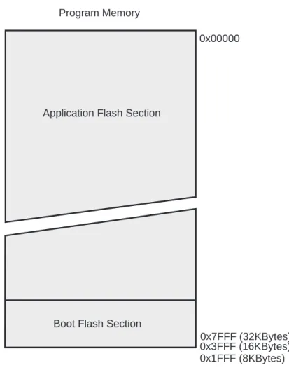
The SPM instruction that writes into the Application Flash memory section must reside in the Boot Program section. Note that the status register is updated after all ALU operations, as specified in the instruction set reference.
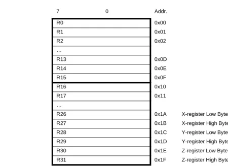
Stack Pointer
SPH and SPL – Stack Pointer High and Low Register
Instruction Execution Timing
Reset and Interrupt Handling
Interrupt Response Time
The interrupt execution response for all enabled AVR interrupts is at least five clock cycles. After five clock cycles, the address of the program vector for the actual interrupt handling routine is executed.
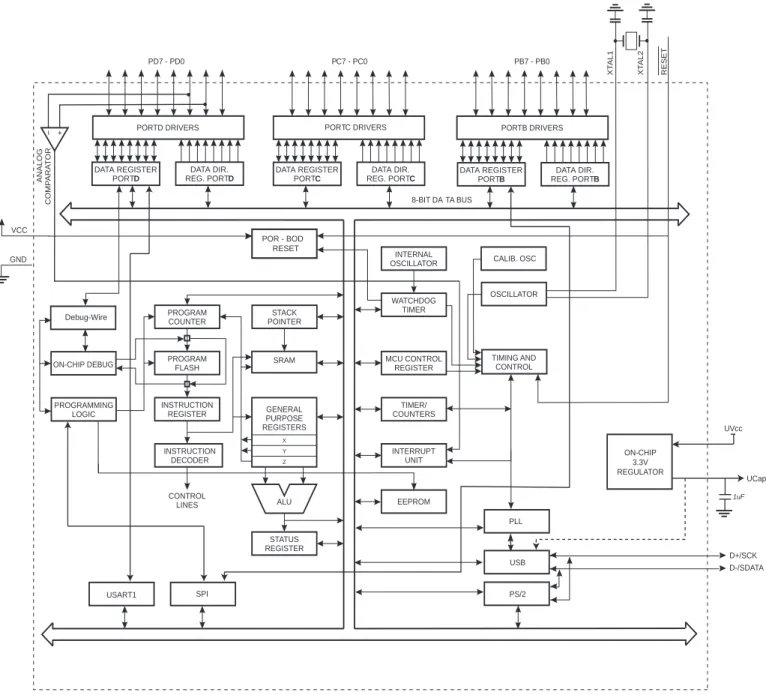
AVR Memories
- In-System Reprogrammable Flash Program Memory
- SRAM Data Memory
- Data Memory Access Times
- EEPROM Data Memory
- EEPROM Read/Write Access
- Preventing EEPROM Corruption
- I/O Memory
- General Purpose I/O Registers
- Register Description
- EEARH and EEARL – The EEPROM Address Register
- EEDR – The EEPROM Data Register
- EECR – The EEPROM Control Register
- GPIOR2 – General Purpose I/O Register 2
- GPIOR1 – General Purpose I/O Register 1Assembly Code Example (1)
- GPIOR0 – General Purpose I/O Register 0
When the EEPROM is read, the CPU is halted for four clock cycles before the next instruction is executed. When the EEPROM is read, the CPU is halted for four cycles before the next instruction is executed.
System Clock and Clock Options
- Clock Systems and their Distribution
- CPU Clock – clk CPU
- I/O Clock – clk I/O
- Flash Clock – clk FLASH
- USB Clock – clk USB
- Clock Switch
- Exemple of use
- Clock switch Algorythm
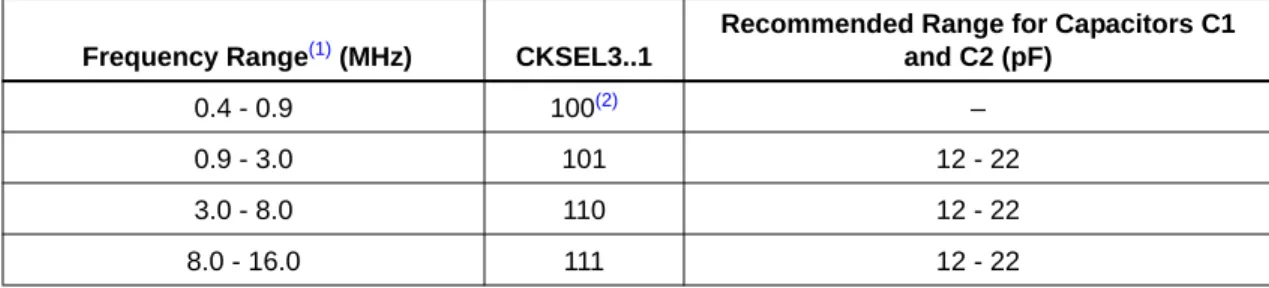
- Clock Sources
- Default Clock Source
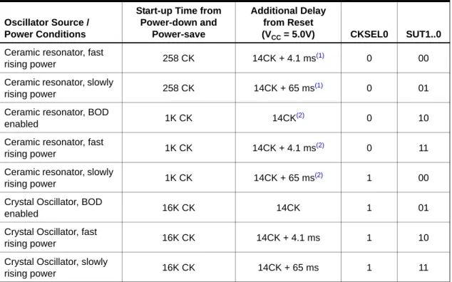
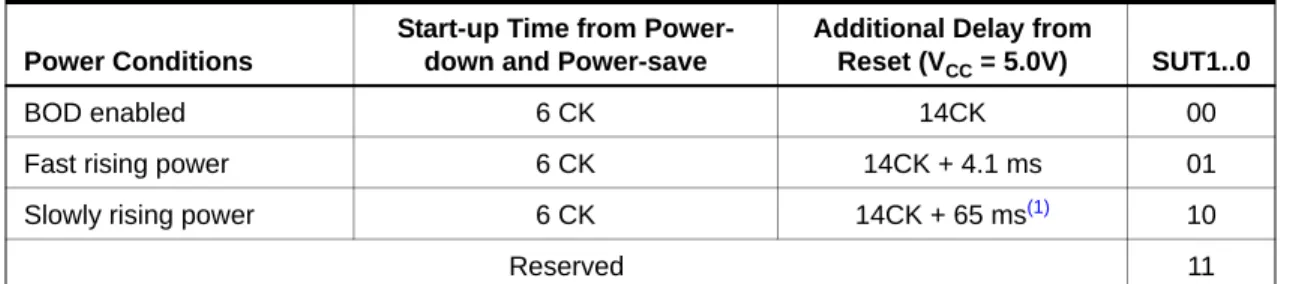
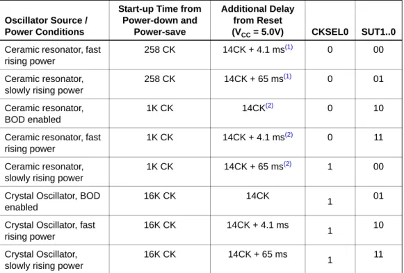
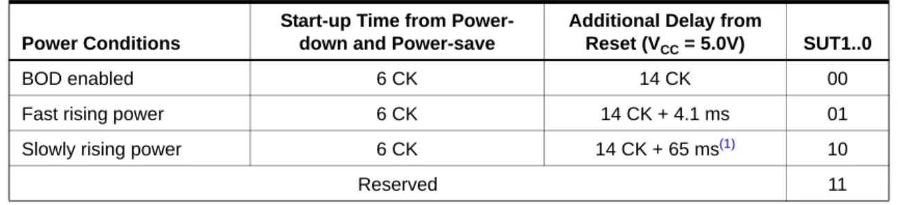
- Clock Startup Sequence
- Low Power Crystal Oscillator
- Full Swing Crystal Oscillator
- Calibrated Internal RC Oscillator
- External Clock
- Clock Output Buffer
- System Clock Prescaler
- Internal PLL for USB interface
- Register Description
- CLKSEL0 – Clock Selection Register 0
- CLKSEL1 – Clock Selection Register 1
- CLKSTA – Clock Status Register
- OSCCAL – Oscillator Calibration Register
- CLKPR – Clock Prescale Register
- PLLCSR – PLL Control and Status Register
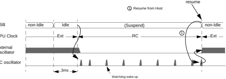
The frequency of the Watchdog Oscillator is voltage dependent, as shown in "Typical Characteristics" on page 273. This value will be used in the next startup of the External Oscillator / Low Power Oscillator.
Power Management and Sleep Modes
- Overview
- Sleep Modes
- Idle Mode
- Power-down Mode
- Power-save Mode
- Standby Mode
- Extended Standby Mode
- Power Reduction Register
- Minimizing Power Consumption
- Analog Comparator
- Brown-out Detector
- Internal Voltage Reference
- Watchdog Timer
- Port Pins
- On-chip Debug System
- Register Description
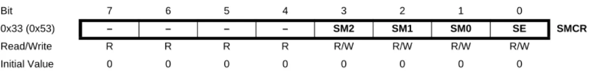
- SMCR – Sleep Mode Control Register
- PRR0 – Power Reduction Register 0
- PRR1 – Power Reduction Register 1
When the USB is re-awakened, the USB must be re-initialized to ensure proper operation. When the USART1 wakes up again, the USART1 must be re-initialized to ensure proper operation.
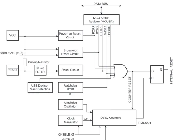
System Control and Reset
- Resetting the AVR
- Reset Sources
- Power-on Reset
- External Reset
- Brown-out Detection
- Watchdog Reset
- USB Reset
- Internal Voltage Reference
- Voltage Reference Enable Signals and Start-up Time
- Watchdog Timer
- Features
- Overview
- Register Description
- MCUSR – MCU Status Register
- WDTCSR – Watchdog Timer Control Register
- WDTCKD – Watchdog Timer Clock Divider Register
This bit is set if the Watchdog Timer times out twice and if the Watchdog Timer is configured for interrupt. This bit is set when the Watchdog Timer first times out and the WDEWIE bit is enabled.
Interrupts
Overview
Interrupt Vectors in ATmega8U2/16U2/32U2
- Moving Interrupts Between Application and Boot Space
When the IVSEL bit in the MCUCR is set, the Interrupt Vectors will be moved to the start of the Boot Flash section. This is also the case if the Reset Vector is in the Application section while the Interrupt Vectors are in the Boot section or vice versa.
Register Description
- MCUCR – MCU Control Register
Note: If Interrupt vectors are placed in the Boot Loader section and Boot Lock bit BLB02 pro-. If Interrupt Vectors are placed in the Application section and Boot Lock bit BLB12 is programmed, interrupts are disabled when running from the Boot Loader section.
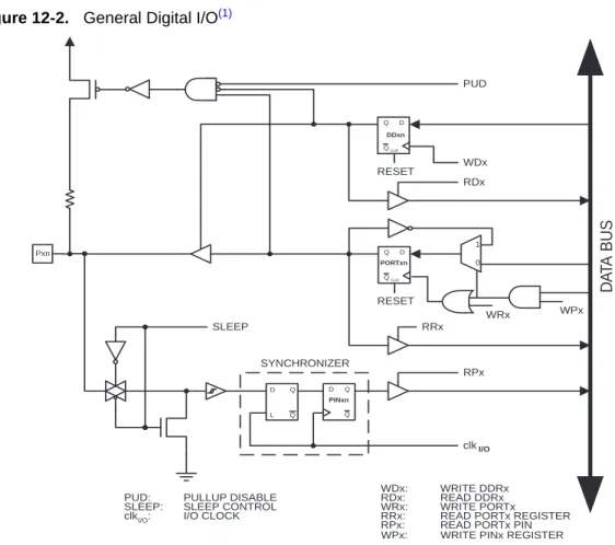
I/O-Ports
- Overview
- Ports as General Digital I/O
- Configuring the Pin
- Toggling the Pin
- Switching Between Input and Output
- Reading the Pin Value
- Digital Input Enable and Sleep Modes
- Unconnected Pins
- Alternate Port Functions
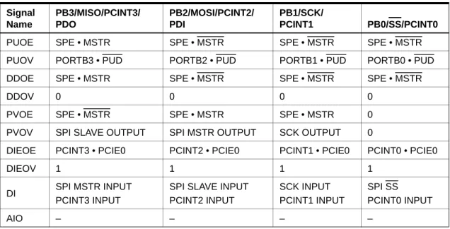
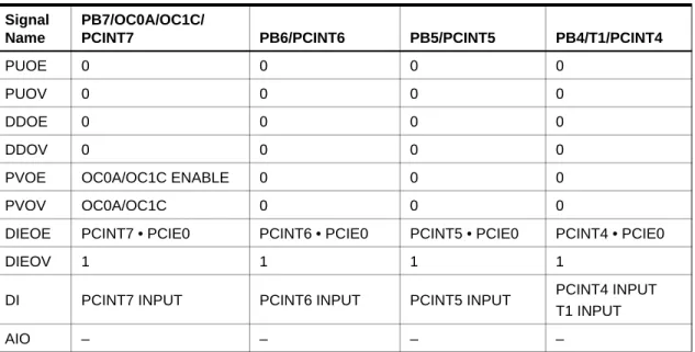
- Alternate Functions of Port B
- Alternate Functions of Port C
- Alternate Functions of Port D
- Register Description for I/O-Ports
- MCUCR – MCU Control Register
- PORTB – Port B Data Register
- DDRB – Port B Data Direction Register
- PINB – Port B Input Pins Address
- PORTC – Port C Data Register
- DDRC – Port C Data Direction Register
- PINC – Port C Input Pins Address
- PORTD – Port D Data Register
- DDRD – Port D Data Direction Register
- PIND – Port D Input Pins Address
PCINT7, Pin Change Interrupt Source 7: The PB7 pin can serve as an external interrupt source. PCINT2, Pin Change Interrupt Source 2: The PB2 pin can serve as an external interrupt source. PCINT8, Pin Change Interrupt Source 8: The PC6 pin can serve as an external interrupt source.
PCINT9, Pin Change Interrupt source 9: PC5 pin can act as an external interrupt source.
External Interrupts
Overview
Register Description
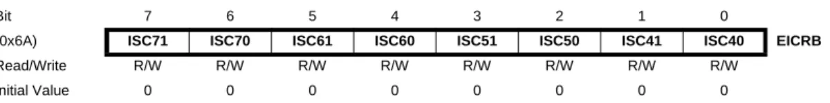
- EICRA – External Interrupt Control Register A
- EICRB – External Interrupt Control Register B
- EIMSK – External Interrupt Mask Register
- EIFR – External Interrupt Flag Register
- PCICR – Pin Change Interrupt Control Register
- PCIFR – Pin Change Interrupt Flag Register
- PCMSK0 – Pin Change Mask Register 0
- PCMSK1 – Pin Change Mask Register 1
When an INT[7:0] bit is written to one and the I bit in the Status Register (SREG) is set (one), the corresponding external pin interrupt is enabled. When the PCIE1/0 bit is set (one) and the I bit in the Status Register (SREG) is set (one), Pin Change interrupt 1/0 is enabled. If PCINT[7:0] is set and the PCIE0 bit in PCICR is set, pin change interrupt is enabled on the corresponding I/O pin.
If PCINT[12:8] is set and the PCIE1 bit in PCICR is set, the pin change interrupt is enabled on the corresponding I/O pin.
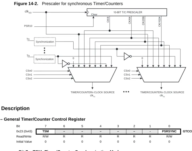
Timer/Counter0 and Timer/Counter1 Prescalers
- Overview
- Internal Clock Source
- Prescaler Reset
- External Clock Source
- Register Description
- GTCCR – General Timer/Counter Control Register
- Features
- Overview
- Registers
- Definitions
- Timer/Counter Clock Sources
- Counter Unit
- Output Compare Unit
- Force Output Compare
- Compare Match Blocking by TCNT0 Write
- Using the Output Compare Unit
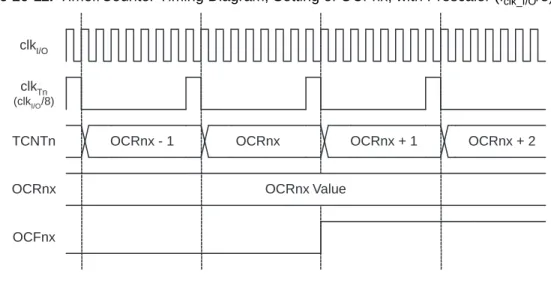
The timer/counter can be clocked internally, via the prescaler or by an external clock source on the T0 pin. The double-buffered output compare registers (OCR0A and OCR0B) are compared to the timer/counter value at all times. The counting sequence is determined by the setting of the WGM01 and WGM00 bits located in the Timer/Counter Control Register (TCCR0A) and the WGM02 bit located in the Timer/Counter Control Register B (TCCR0B).
The timer/counter overflow flag (TOV0) is set according to the mode of operation selected by the WGM0[2:0] bits.
DATA BUS
Compare Match Output Unit
- Compare Output Mode and Waveform Generation
When referring to the OC0x state, the reference refers to the OC0x internal register, not the OC0x pin. However, the direction of the OC0x pin (input or output) is still controlled by the data direction register (DDR) for the port pin. The logic design of the output compare pins allows the OC0x state to be initialized before the output is enabled.
For all modes, the COM0x[1:0] = 0 sets the waveform generator that no action should be performed on the OC0x register on the next Compare Match.
Modes of Operation
- Normal Mode
- Clear Timer on Compare Match (CTC) Mode
- Fast PWM Mode
- Phase Correct PWM Mode
If the new value written to OCR0A is lower than the current value of TCNT0, the counter will miss the Compare Match. In fast PWM mode, the counter is incremented until the counter value matches the TOP value. In phase-correct PWM mode, the counter is incremented until the counter value matches TOP.
The interrupt flag can be used to generate an interrupt every time the counter reaches the LOW value.
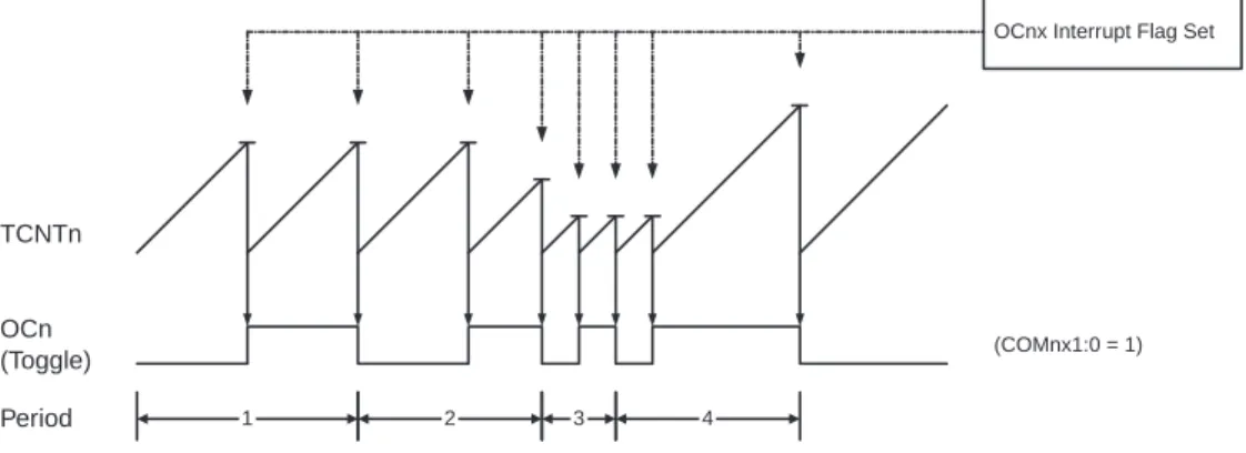
Timer/Counter Timing Diagrams
The PWM waveform is generated by clearing (or setting) the OC0x Register at the Compare Pass between OCR0x and TCNT0 when the counter increments, and setting (or clearing) the OC0x Register at the Compare Pass between OCR0x and TCNT0 when the counter is counting down. At the very beginning of period 2 in Figure 15-7, OCnx has a transition from high to low even though there is no Compare Match. When the OCR0A value is MAX, the OCn pin value is the same as the result of a comparison counting down.
To ensure symmetry around BOTTOM, the OCn value at MAX must match the result of an enumerated Compare Match.
Register Description
- TCCR0A – Timer/Counter Control Register A
- TCCR0B – Timer/Counter Control Register B
- TCNT0 – Timer/Counter Register
- OCR0A – Output Compare Register A
- OCR0B – Output Compare Register B
- TIMSK0 – Timer/Counter Interrupt Mask Register
- TIFR0 – Timer/Counter 0 Interrupt Flag Register
When the OCIE0B bit is written to one and the I bit in the status register is set, the Timer/Counter Compare Match B interrupt is enabled. The corresponding interrupt is executed if a Compare Match occurs in Timer/Counter0, i.e. when the OCF0A bit is set in the Timer/Counter 0 Interrupt Flag Register – TIFR0. When the I bit in SREG, OCIE0B (Timer/Counter Compare B Match Interrupt Enable) and OCF0B are set, the Timer/Counter Compare Match Interrupt is executed.
When the I bit in SREG, OCIE0A (Timer/Counter0 Compare Match Interrupt Enable) and OCF0A are set, the Timer/Counter0 Compare Match Interrupt is executed.
![Table 15-4 shows the COM0A1:0 bit functionality when the WGM0[2:0] bits are set to phase cor- cor-rect PWM mode.](https://thumb-ap.123doks.com/thumbv2/123dok/10669285.0/103.918.244.863.164.368/table-shows-com0a1-functionality-wgm0-bits-phase-rect.webp)
Features
Overview
- Registers
- Definitions
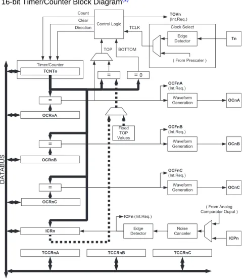
The Timer/Counter (TCNTn), Output Compare Registers (OCRnA/B/C), and Input Capture Register (ICRn) are all 16-bit registers. The Timer/Counter Control Registers (TCCRnA/B/C) are 8-bit registers and have no CPU access restrictions. The double-buffered Output Compare Registers (OCRnA/B/C) are compared to the Timer/Counter value all the time.
The Input Capture Register can capture the timer/counter value upon a given external (edge-triggered) event on either the Input Capture pin (ICPn) or on the Analog Comparator pins (see . “Analog Comparator” on page 223). Input Capture unit includes a digital filtering unit (Noise Canceler) to reduce the chance of capturing noise spikes.
Accessing 16-bit Registers
- Reusing the Temporary High Byte Register
The following code examples show how to do an atomic read of the contents of the TCNTn register. Reading any of the OCRnA/B/C or ICRn registers can be done using the same principle. The following code examples show how to do an atomic write of the contents of the TCNTn register.
Writing any of the OCRnA/B/C or ICRn registers can be done using the same principle.
Timer/Counter Clock Sources
The assembly code example requires register pair r17:r16 to contain the value to be written to TCNTn. If you write to more than one 16-bit register where the high byte is the same for all registers written, the high byte only needs to be written once. Note, however, that the same rule of atomic action described earlier also applies in this case.
Counter Unit
Input Capture Unit
- Input Capture Trigger Source
- Noise Canceler
- Using the Input Capture Unit
Reading the 16-bit value in the input capture register (ICRn) is done by first reading the low byte (ICRnL) and then the high byte (ICRnH). Both the input capture pin (ICPn) and the analog comparator output (ACO) inputs are sampled using the same technique as for the Tn pin (Figure 14-1 on page 88). The noise reducer is enabled by setting the Input Capture Noise Reducer bit (ICNCn) in the Timer/Counter Control Register B (TCCRnB).
After an edge change, the Input Capture Flag (ICFn) must be cleared by software (writes a logic one to the I/O bit location).
Output Compare Units
- Force Output Compare
- Compare Match Blocking by TCNTn Write
- Using the Output Compare Unit
For frequency measurement only, clearing the ICFn flag is not required (if an interrupt handler is used). The OCRnx register is double buffered when using one of twelve pulse width modulation (PWM) modes. The double buffering synchronizes the update of the OCRnx comparison register with TOP or BOTTOM of the count sequence.
The contents of the OCR1x (Buffer or Compare) Register are only changed by a write operation (the Timer/Counter does not automatically update this register like the TCNT1 and ICR1 Register).
Compare Match Output Unit
- Compare Output Mode and Waveform Generation
For fast PWM mode, see Table 16-2 on page 130, and for phase correct and phase and frequency correct PWM, see Table 16-3 on page 131.
Modes of Operation
- Normal Mode
- Clear Timer on Compare Match (CTC) Mode
- Fast PWM Mode
- Phase Correct PWM Mode
- Phase and Frequency Correct PWM Mode
The phase correct PWM mode, like the phase and frequency correct PWM mode, is based on a dual-slope operation. The phase and frequency correct PWM mode, like the phase correct PWM mode, is based on a dual-slope operation. The PWM resolution for the phase and frequency correct PWM mode can be defined by ICRn or OCRnA.
The timing diagram for the phase-correct and frequency-correct PWM mode is shown in Figure 16-9.
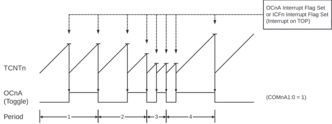
Timer/Counter Timing Diagrams
In PWM mode, with the correct phase and frequency, the comparator units enable the generation of PWM waveforms on the OCnx pins. Extreme values for the OCRnx register represent special cases when generating PWM output waveforms in phase-correct PWM mode. If OCRnx is set to BOTTOM, the output will be continuously low and if set to TOP, the output will be set high for non-inverted PWM mode.
When using phase and frequency correct PWM mode, the OCRnx register is updated at the bottom.
Register Description
- TCCR1A – Timer/Counter1 Control Register A
- TCCR1B – Timer/Counter1 Control Register B
- TCCR1C – Timer/Counter1 Control Register C
- TCNT1H and TCNT1L – Timer/Counter1
- OCR1AH and OCR1AL – Output Compare Register 1 A
- OCR1BH and OCR1BL – Output Compare Register 1 B
- OCR1CH and OCR1CL – Output Compare Register 1 C
- ICR1H and ICR1L – Input Capture Register 1
- TIMSK1 – Timer/Counter1 Interrupt Mask Register
Compare Output Mode, non-PWM COMnA1/COMnB1/. 0 0 Normal port operation, OCnA/OCnB/OCnC. 0 1 Switch OCnA/OCnB/OCnC on comparison match. When the Noise Canceler is enabled, the input from the Input Capture Pin (ICPn) is filtered. The input capture is therefore delayed by four Oscillator cycles when the squelch is enabled.
IThe Input Capture is updated with the counter (TCNTn) value every time an event occurs on the ICPn pin (or optionally on the Analog Comparator output for Timer/Counter1).
![Table 16-2 shows the COMnx[1:0] bit functionality when the WGMn[3:0] bits are set to the fast PWM mode.](https://thumb-ap.123doks.com/thumbv2/123dok/10669285.0/130.918.230.863.137.337/table-shows-comnx-functionality-wgmn-bits-fast-pwm.webp)
OCIEnC: Timer/Countern, Output Compare C Match Interrupt Enable
- TIFR1 – Timer/Counter1 Interrupt Flag Register
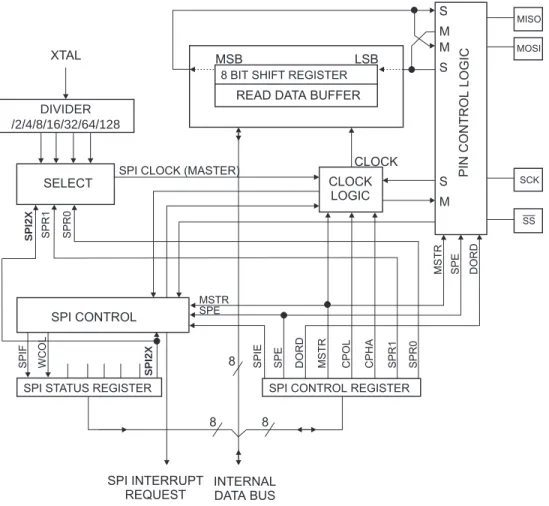
- SPI – Serial Peripheral Interface
- Features
- Overview
- SS Pin Functionality
- Data Modes
- Register Description
- USART
- Features
- Overview
- Clock Generation
- Frame Formats
- USART Initialization
- Data Transmission – The USART Transmitter
- Data Reception – The USART Receiver
- Asynchronous Data Reception
- Multi-processor Communication Mode
- Hardware Flow Control
- Register Description
- Examples of Baud Rate Setting
- USART in SPI Mode
- Features
- Overview
- Clock Generation
- SPI Data Modes and Timing
- Frame Formats
- Data Transfer
- Register Description
- AVR USART MSPIM vs. AVR SPI
- USB Controller
- Features
- Overview
- USB Module Powering Options
- General Operating Modes
- Power modes
- Memory management
- PAD suspend
- D+/D- Read/write
- USB Software Operating modes
When the DORD bit is written to one, the data word's LSB is sent first. When the DORD bit is written to zero, the MSB of the data word is sent first. When disabled (i.e. the RXENn is set to zero) the receiver will no longer override the normal function of the RxDn port pin.
The receiver FIFO buffer will be flushed when the receiver is disabled, which means the buffer will be flushed. Pin control is different due to only main USART operation in MSPIM mode. A comparison of USART in MSPIM mode and SPI pins is shown in Table 19-4 on page 184.
WAKEUPI
Registers Description
- USBCON – USB General Control Registers
- UPOE – USB Software Output Enable register
- REGCR – Regulator Control Register
Writing this bit to one enables the USB controller and the USB data buffers (D+ and D-). Writing this bit to one disables the internal clock for the USB controller, thereby freezing it. Writing this bit to zero unfreezes the USB controller and allows full operation of the USB interface.
The possible configurations of these bits allow USB buffers to be enabled or disabled directly by the drive software.
USB Device Operating modes
- Overview
- Power-on and reset
- Endpoint reset
- USB reset
- Endpoint selection
- Endpoint activation
- Address Setup
- Suspend, Wake-up and Resume
- Detach
An endpoint reset can be associated with clearing the data switch instruction (RSTDT bit) in response to the CLEAR_FEATURE USB command. This is done by setting the EPNUM[2:0] bits (in the UENUM register) with the number of the endpoint to be managed by the CPU. The endpoint is reset until the EPEN bit is set.
As long as the endpoint is not configured correctly (CFGOK cleared), the hardware does not acknowledge the packets sent by the host.