This book is a comprehensive survey of the principles and techniques of modern digital systems. Sections of the text that cover the special aspects of a language are clearly marked with a color bar in the margin.
Chapter Organization
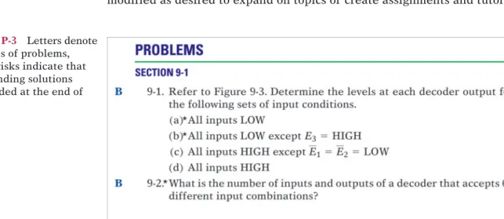
Problems for which solutions are printed in the back of the text or on the accompanying CD-ROM are marked with an asterisk (see Figure P-3). The circuit diagrams of many of the figures throughout the text are captured as input files for this popular simulation tool.
Specific Changes
All the problems at the end of Chapter 7 have been rewritten to reinforce the concepts. The technique of using a MUX to implement SOP expressions has been explained in a more structured way as a self-study exercise in the end-of-chapter problems.
Retained Features
Supplements
Solutions to Chapter 7 problems include some large graphics and HDL files that are not published in the back of the book but are available on the included CD-ROM. Laboratory Manual: A Problem Solving Approach. Written by Jim DeLoach and Frank Ambrosio, this manual is presented with an analysis and problem-solving approach and has been fully updated for this edition of the text.
ACKNOWLEDGMENTS
- Flip-Flops and Related Devices 208 CHAPTER 6 Digital Arithmetic: Operations and Circuits 296
- Integrated-Circuit Logic Families 488
- Digital System Projects Using HDL 676 CHAPTER 11 Interfacing with the Analog World 718
- Programmable Logic Device Architectures 868
- Number Systems and Codes 24
- Describing Logic Circuits 54
- Combinational Logic Circuits 118
- Flip-Flops and Related Devices 208
- Digital Arithmetic
- Integrated-Circuit Logic Families 488
- Digital System Projects Using HDL 676
- Interfacing with the Analog World 718
- Programmable Logic Device
Instructor's Resource Manual. This manual contains detailed solutions to all the problems at the end of the chapter in this textbook. Lab Solutions Manual. Detailed lab results for both lab manuals can be found in this manual.
Glossary 898
Answers to Selected Problems 911 Index of ICs 919
Index 922
Digital Systems
Principles and Applications
OUTLINE
OBJECTIVES
INTRODUCTION
1-1 NUMERICAL REPRESENTATIONS
Analog Representations
Digital Representations
Due to the discrete nature of digital representations, there is no ambiguity when reading the value of a digital quantity, whereas the value of an analog quantity is often open to interpretation. In practice, when we take a measurement of an analog quantity, we always "round" to a convenient level of precision.
1-2 DIGITAL AND ANALOG SYSTEMS
Answers to review questions can be found at the end of the chapter in which they appear. Among the more familiar digital systems are digital computers and calculators, digital audio and video equipment, and the telephone system – the largest digital system in the world.
Advantages of Digital Techniques
For example, the amplitude of the output signal to the speaker in a radio receiver can have any value between zero and its maximum limit. Other common analog systems are audio amplifiers, magnetic tape recording and playback equipment, and a simple light dimmer switch.
Limitations of Digital Techniques
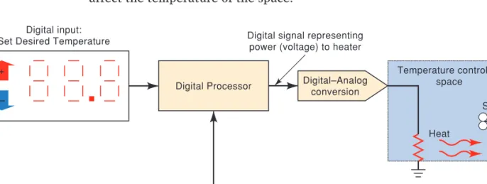
This voltage is applied to a heating element, which will produce heat related to the voltage applied and affect the temperature of the space. The position of the metal object was measured by passing an infrared light beam over the magnetic field.
The Future Is Digital
The trend in most systems is to digitize the signal as early as possible and convert back to analog as late as possible as the signals flow through the system.
1-3 DIGITAL NUMBER SYSTEMS
Decimal System
Decimal Counting
Another characteristic of the decimal system is that by using only two decimal places, we can count through different numbers (0 to 99).* With three places we can count up to 1000 numbers (0 to 999), and so in a row. In general, with Places or digits, we can count up to 10N different numbers, starting and including zero.
Binary System
Note that in the previous operation the subscripts (2 and 10) were used to indicate the base in which the particular number is expressed. In the binary system, the term binary digit is often abbreviated to the term bit, which we will use from now on.
Binary Counting
This convention is used to avoid confusion whenever more than one number system is used. Thus, in the number expressed in Figure 1-5 there are four bits to the left of the binary point, representing the integer part of the number, and three bits to the right of the binary point, representing the fractional part.
1-4 REPRESENTING BINARY QUANTITIES
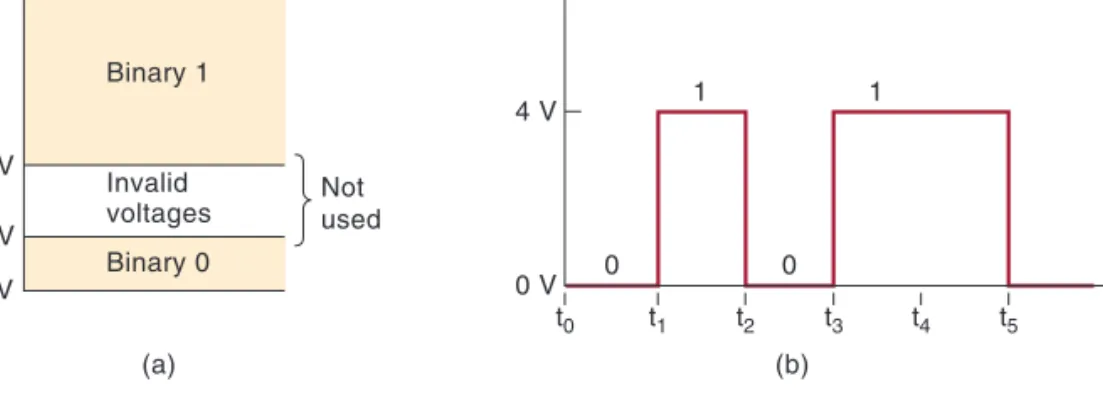
The gate will only open if a matching bit pattern is set in the receiver and transmitter. In electronic digital systems, binary information is represented by voltages (or currents) present at the inputs and outputs of various circuits.
Digital Signals and Timing Diagrams
1-5 DIGITAL CIRCUITS/LOGIC CIRCUITS
To illustrate, Figure 1-9 shows a typical digital circuit with input vi and output vo. The output is shown for two different input signal waveforms. Note that vo is the same for both cases because the two input waveforms, although differing in their exact voltage levels, are at the same binary levels.
Logic Circuits
Digital Integrated Circuits
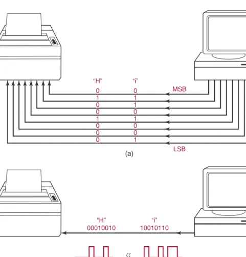
1-6 PARALLEL AND SERIAL TRANSMISSION
Note that in this presentation, the least significant bit appears on the left because it was sent first. On the other hand, parallel requires more signal lines connected between the sender and receiver of binary data than serial.
1-7 MEMORY
The main trade-off between parallel and series representations is speed versus circuit simplicity. Transferring binary data from one part of a digital system to another can be done more quickly using parallel representation because all bits are transferred simultaneously, while serial representation transfers one bit at a time.
1-8 DIGITAL COMPUTERS
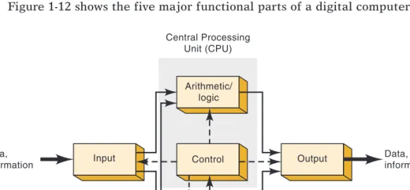
Major Parts of a Computer
All arithmetic calculations and logical decisions are performed in this unit, which can then send results to the memory unit to be stored. This device takes data from the memory device and prints, displays, or otherwise presents the information to the operator (or the process in the case of a process control computer).
Central Processing Unit (CPU)
Through this device, a complete set of instructions and data is fed into the computer system and into the memory device to be stored until needed. It then sends appropriate signals to all the other devices to cause the specific instruction to be executed.
SUMMARY
Microcontrollers generally have all the elements of a complete computer (CPU, memory, and input/output ports) all contained in a single integrated circuit. You can find them built into your kitchen appliances, entertainment devices, photocopiers, vending machines, automated manufacturing equipment, medical instruments and much, much more. So you see, even people who don't have a personal computer or use one at work or school use microcomputers every day, because so many modern consumer electronics, appliances, office equipment, and more are built around embedded microcontrollers.
IMPORTANT TERMS*
PROBLEMS
AND 1-8
ANSWERS TO SECTION REVIEW QUESTIONS
The decimal system is important because it is universally used to represent quantities outside of a digital system. This means that there will be situations where decimal values need to be converted to binary before being entered into the digital system.
2-1 BINARY-TO-DECIMAL CONVERSIONS
2-2 DECIMAL-TO-BINARY CONVERSIONS
Repeated Division
CALCULATOR HINT
Counting Range
2-3 HEXADECIMAL NUMBER SYSTEM
Hex-to-Decimal Conversion
Note that in the second example, the value 10 was substituted for A and the value 15 for F in the conversion to decimal.
Decimal-to-Hex Conversion
Note again that the remainders of the dividing processes form the digits of the hexation number. If a calculator is used to perform the divisions in the conversion process, the results will include a decimal fraction instead of a remainder.
Hex-to-Binary Conversion
Note also that any residue that is greater than 9 is represented by the letters A through F.
Binary-to-Hex Conversion
Counting in Hexadecimal
Note that when there is a 9 in a digit position, it becomes an A when incremented.
Usefulness of Hex
Summary of Conversions
2-4 BCD CODE
This means that conversions between decimal and binary systems are often performed. We have seen that conversions between decimal and binary values can become long and complicated for large numbers.
Binary-Coded-Decimal Code
For this reason, a way of encoding decimal numbers that combines some features of both the decimal and the binary systems is used in certain situations.
Comparison of BCD and Binary
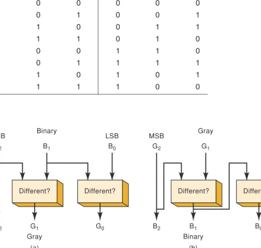
2-5 THE GRAY CODE
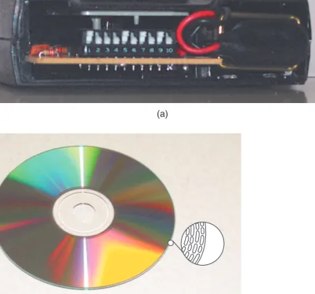
The next binary bit is found by comparing the left binary bit with the corresponding gray code bit. The most common use of the Gray code is in shaft position encoders as shown in Figure 2-3.
2-6 PUTTING IT ALL TOGETHER
2-7 THE BYTE, NIBBLE, AND WORD Bytes
EXAMPLE 2-9 What is the largest decimal value that can be represented in binary using two bytes. EXAMPLE 2-12 What is the hex value of the least significant nibble of the binary number 1001 0101.
Nibbles
Words
2-8 ALPHANUMERIC CODES
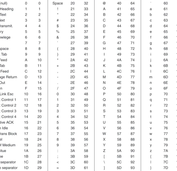
ASCII Code
A computer also uses ASCII internally to store the information that an operator types into the computer's keyboard. Determines the binary strings that will be entered into memory when the operator types the following C statement:.
2-9 PARITY METHOD FOR ERROR DETECTION
Most modern digital equipment is designed to be relatively error-free, and the probability of errors such as those shown in Figure 2-4 is very small. For this reason, many digital systems use some method to detect (and sometimes correct) errors.
Parity Bit
When the receiving circuit receives this code, it will check that the code contains an odd number of 1s (including the parity bit). When the parity method is used, the sender and receiver must agree in advance whether odd or even parity is used.
2-10 APPLICATIONS
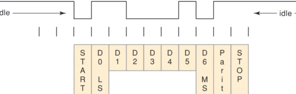
A typical asynchronous transmission of a seven-bit ASCII code for the hash # (23 Hex) with even parity is shown in Figure 2-5. An alphanumeric code is a code that uses groups of bits to represent all the different characters and functions that make up a typical computer's keyboard.
P ROBLEMS 47
IMPORTANT TERMS
AND 2-2
Take each four-bit binary number in the order it is written and write the equivalent hexadecimal character without doing the math by hand or with a calculator. How many bits are required to represent decimal numbers in the range 0 to 999 using (a) flat binary code.
P ROBLEMS 49
AND 2-9
Write the binary number that results from increasing each of the following numbers by one. We will see how the operation of the various logic gates and the more complex circuits formed from combinations of logic gates can be described and analyzed using Boolean algebra.
3-1 BOOLEAN CONSTANTS AND VARIABLES
3-2 TRUTH TABLES
In a similar way, the table shows what happens to the output state for any set of input conditions. Again, each table lists all possible combinations of input logic levels on the left, with the resultant logic level for the output on the right.
3-3 OR OPERATION WITH OR GATES
In this expression, the character does not stand for ordinary addition; it stands for the OR operation. The OR operation is equivalent to ordinary addition, except in the case where A and B are both 1; The OR operation does not produce. In boolean algebra, 1 is as high as we go, so we can never get a result greater than 1.
OR Gate
Using the Boolean algebra language, the output x can be expressed as where it must be emphasized again that the represents the OR operation. Thus, the output of each OR gate can be expressed as the OR combination of the various inputs.
Summary of the OR Operation
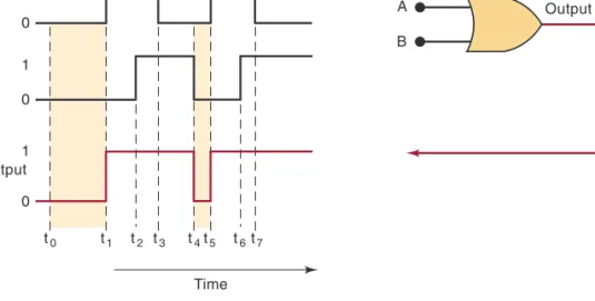
When this happens, the output of the OR gate also becomes a value in this interval, as evidenced by the bump or point in the output waveform at t1. With Cinput HIGH at t1, the output of the OR gate will remain HIGH regardless of what is happening at the other inputs, because any input HIGH will hold an output of the OR gate HIGH.
3-4 AND OPERATION WITH AND GATES
Because these inputs make their transitions at about the same time, and since these transitions take a certain amount of time, there is a short interval where these OR gate inputs are both in the undefined range between 0 and 1. What would happen? with the output disturbance in Figure 3.6 if input Csat is in the HIGH state while A and B change at time t1.
AND Gate
The expression is read as "x equals A AND B," meaning that x will be 1 only when Aand Bare are both 1. For the case when three inputs are ANDed, we have This is read as "equal to AEN BAND C," meaning that x will only be 1 when Aand Band Care is all 1.
Summary of the AND Operation
The output of an AND gate is defined with the understanding that it will be HIGH only when all inputs are HIGH at the same time. Output xw will be at 1 only when A and Bare are both HIGH at the same time.
3-5 NOT OPERATION
NOT Circuit (INVERTER)
Summary of Boolean Operations
3-6 DESCRIBING LOGIC CIRCUITS ALGEBRAICALLY
This AND output is connected as an input to an OR gate along with C, the other input. OR gates operate on their inputs so that their output is the sum of the OR inputs.
Operator Precedence
This circuit has three inputs, A, B, and C, and a single output, x. By using the Boolean expression for each gate, we can easily determine the expression for the output. Thus, we can express the OR output as (This final expression could also be written as because it does not matter which term of the OR sum is written first.).
Circuits Containing INVERTERs
In Figure 3-14(b), the output of the OR gate is equal to AB and is fed through the INVERTER. The expression means that A is ORed with B and then their sum is OR reversed, while the expression indicates that A is reversed and Bis is reversed and the results are then ORed together.
3-7 EVALUATING LOGIC-CIRCUIT OUTPUTS
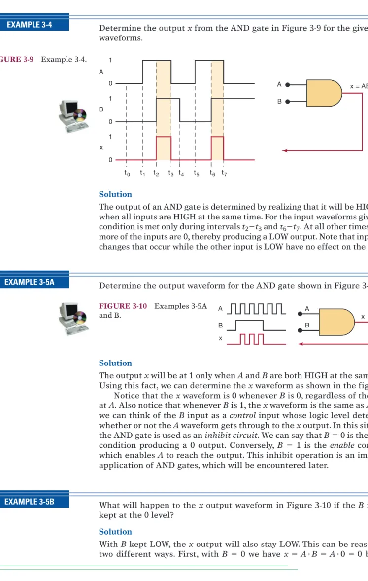
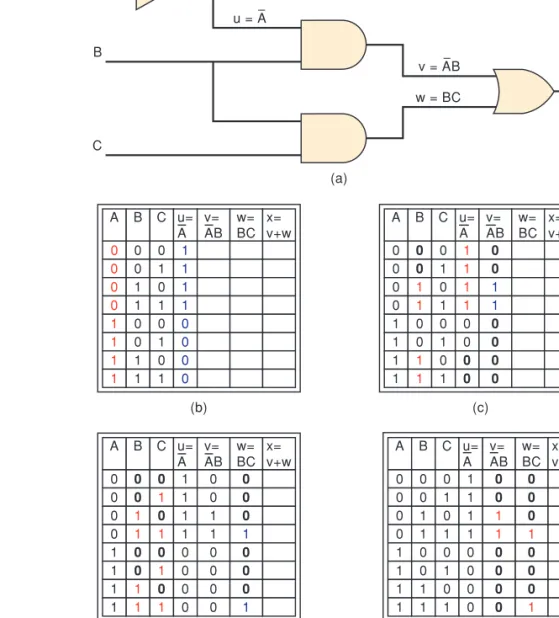
Also notice in Figure 3-15(a) that the input variable A is connected as an input to two different gates. For practice, determine the outputs of both circuits in Figure 3-15 for the case where all inputs are 1.
Analysis Using a Table
The next step is to fill in the values for column fixed in Figure 3-16(c). Since the x output will be HIGH when it is HIGH or HIGH, as shown in Figure 3-16(e).
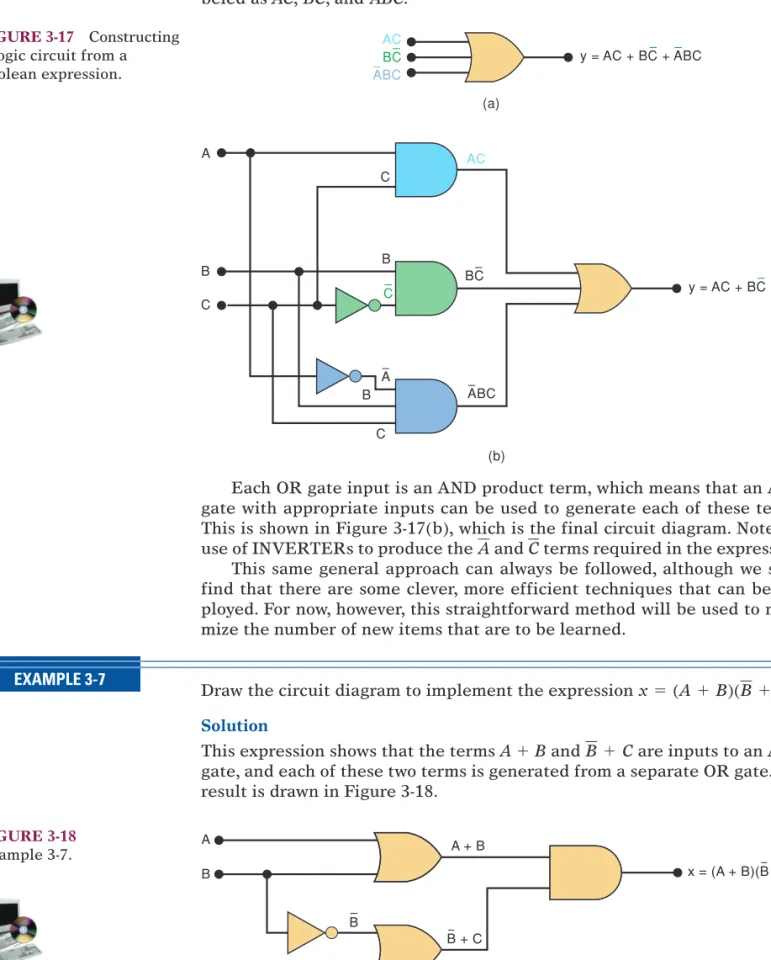
3-8 IMPLEMENTING CIRCUITS FROM BOOLEAN EXPRESSIONS
Each OR gate input is an AND product term, meaning that an AND gate with appropriate inputs can be used to generate each of these terms. This expression shows that the terms ABand are inputs to an AND gate, and each of these two terms is generated from a separate OR gate.
3-9 NOR GATES AND NAND GATES
NOR Gate
One way to determine the output OR waveform is to first find the output OR waveform and then invert it (change all 1s to 0s and vice versa). The expression at the NOR output is then fed through an INVERTER for production.
NAND Gate
The NOR gate has inputs 1 and 0 to produce an output of 0 (an OR would have produced an output of 1). Thus, the NAND gate has input levels of 0, 1, and 1 to produce an output of 1 (an AND would have produced an output of 0).
3-10 BOOLEAN THEOREMS
We also know that the output of an AND gate will be 0 whenever any input is 0, regardless of the level at the other input. Theorem (8) can be proved similarly, or we can simply reason that at all times each xor must be at level 1, so we are always ORing a 0 and a 1, which always results in a 1.
Multivariable Theorems
Theorem (13) is the distributive law which states that an expression can be expanded by multiplying term by term just as in ordinary algebra. That is, if we have a sum of two (or more) terms, each containing a common variable, the common variable can be worked out just as in ordinary algebra.
3-11 DEMORGAN’S THEOREMS
This can be thought of as breaking the large converter sign in the middle and changing the AND sign ( ) to an OR sign. Here we see that the sign of the large modifier is broken at two points in the expression, and the sign of the operator is changed to its opposite.
Implications of DeMorgan’s Theorems
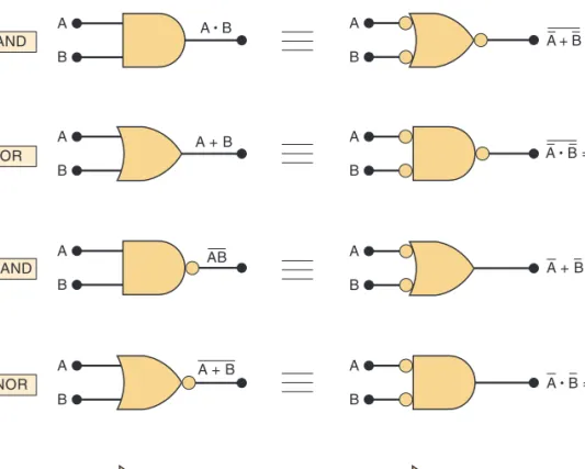
The left side of the equation can be implemented by a NAND gate with xand y inputs. The right side can be implemented by first inverting the x and yand inputs then putting them through an OR gate. The OR gate with INVERTERS on each of its inputs is equivalent to the NAND gate.
3-12 UNIVERSALITY OF NAND GATES AND NOR GATES
Here, NAND gates 1 and 2 are used as INVERTERS to invert the inputs so that the final output can be simplified to xA using DeMorgan's theorem. Here, NOR gates 1 and 2 are used as INVERTERS to invert the inputs so that the final output is the one that can be simplified.
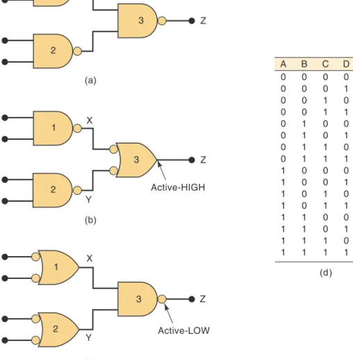
3-13 ALTERNATE LOGIC-GATE REPRESENTATIONS
None of the standard symbols have bubbles on their input, and all alternate symbols do. NAND and NOR gates are inverting gates, so both the standard and alternate symbols have a bell on either the input or the output for each.
Logic-Symbol Interpretation
The standard and alternate symbols for each port represent the same physical circuit; there is no difference in the circuits represented by the two symbols. AND and OR gates are non-rotating gates, so they will have alternate symbols for each of the input and output bubbles.
Summary
3-14 WHICH GATE REPRESENTATION TO USE
The circuit in Figure 3-36(a) contains three NAND gates connected to produce an output Z that depends on inputs A, B, C, and D. The circuit diagram uses the standard symbol for each of the NAND gates. The resulting truth table is the same as that obtained for the circuit diagram of Figure 3-36(b).
Which Circuit Diagram Should Be Used?
This description can be translated into truth table form by making Z0 for all cases where at least one of the Aor Binputs is LOW and at the same time at least one of the Cor Dinputs is LOW.
Bubble Placement
The NOR gate symbol must be changed to the alternate symbol with a non-bubble output (active-HIGH) to match the non-bubble input of AND gate 2, as shown in Figure 3-37(b). Note that the circuit now has non-bubble outputs connected to the non-bubble inputs of port 2.
Analyzing Circuits
A more efficient method is to interpret the circuit diagram using the ideas we have developed in the last two sections. Putting all this together, DRIVE will be HIGH when A1A2A3A4 A5A6A71 and A00 and either INor OUTor both are 1.
Asserted Levels
Labeling Active-LOW Logic Signals
Labeling Bistate Signals
S ECTION 3-15/ IEEE/ANSI S TANDARD L OGIC S YMBOLS 95
Use the method of Examples 3-22 and 3-23 to determine the input conditions necessary to activate the output of the circuit in Figure 3-37(b). What will be the output level in Figure 3-38(b) when all the inputs are asserted.
3-15 IEEE/ANSI STANDARD LOGIC SYMBOLS
The “&” in the AND symbol means that the output goes to the active HIGH state when all inputs are in their active HIGH state. The “ ” inside the OR gate means that the output goes to the active state (HIGH) when one or more inputs are in their active state (HIGH).
Traditional or IEEE/ANSI?
The "1" inside the INVERTER symbol indicates a device with only one input; the triangle on the output indicates that the output will go to its active-LOW state when that one input is in its active-HIGH state. The rectangular symbols for the NAND and the NOR are the same as those for the AND and the OR, respectively, with the addition of the small inversion triangle on the output.
3-16 SUMMARY OF METHODS TO DESCRIBE LOGIC CIRCUITS
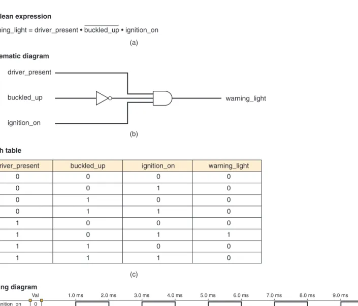
A separate notation within each rectangular symbol describes the logical connection between inputs and outputs. If the driver is present AND the driver is NOT tight AND the ignition key is on, THEN turn on the warning light.
3-17 DESCRIPTION LANGUAGES VERSUS PROGRAMMING LANGUAGES*
There are many other ways we can represent the logic of this decision. The important point here is that we need ways to describe and communicate how digital systems work.
VHDL and AHDL
Of course, we cannot cover every possible way of describing a logic circuit, but we need to understand the most common methods in order to communicate with others in the profession. Unlike VHDL, this language is not intended to be used as a universal language for describing any logic circuit.
Computer Programming Languages
It is intended to be used for programming complex digital systems in Altera PLDs in a language generally considered easier to learn, yet very similar to VHDL. All of the examples in this text will use the Altera MAXPLUS II or Quartus II software to develop both AHDL and VHDL design files.
3-18 IMPLEMENTING LOGIC CIRCUITS WITH PLDs
The role of the hardware description language is to provide a concise and convenient way for the designer to describe the operation of the circuit in a format that a personal computer can handle and store conveniently. Our goal is to learn enough of HDL to be able to communicate with others and perform simple tasks.
3-19 HDL FORMAT AND SYNTAX
The set of statements that describe the operation of the AHDL circuit is contained in the logic section between the keywords BEGIN and END. In this example, the operation of the hardware is described by a very simple Boolean algebra equation that states that the output (y) is assigned the logic level produced by a AND b () .
BOOLEAN DESCRIPTION USING AHDL
Something must enclose the circuit that we are trying to describe, in the same way that a block diagram encloses everything that makes up that part of the design. All statements (there is only one in this example) between BEGIN and END are evaluated constantly and simultaneously.
BOOLEAN DESCRIPTION USING VHDL
3-20 INTERMEDIATE SIGNALS
AHDL BURIED NODES
In the hardware description on line 13, the intermediate variable is assigned a value (connected) and then m is used in the second statement on line 14 to assign a value to y (connected). Remember that the assignment statements are concurrent, so the order in which they are issued does not matter. For human readability, it may seem more logical to assign values to intermediate variables before using them in other assignment statements, as shown here.
VHDL LOCAL SIGNALS
AND 3-12
Then write the output expression for the new circuit, simplify it using DeMorgan's theorems, and compare it to the expression for the original circuit. Then write the expression for the new circuit, simplify it using DeMorgan's theorems, and compare it to the expression for the original circuit.
AND 3-14
The first item that appears at the top of an HDL list is the functional description. f) The type of an object indicates whether it is an input or an output. g). Here the light is an LED that will be ON (conducting) when the NOR gate output is LOW.
AHDL
Use Boolean algebra and the Karnaugh map as tools to simplify and design logic circuits. In the latter parts of this chapter, we will expand our knowledge of programmable logic devices and hardware description languages.
4-1 SUM-OF-PRODUCTS FORM
To make this material as practical as possible, we will first present some of the basic characteristics of logic-gate ICs in the TTL and CMOS logic families, along with a description of the most common types of errors that occur in digital ICs -orbit. The concept of programmable hardware connections will be reinforced and we will provide more details on the role of the development system.
Product-of-Sums
You will learn the steps involved in designing and developing today's digital systems. Finally, several control structures will be explained, along with some guidance on their appropriate use.
4-2 SIMPLIFYING LOGIC CIRCUITS
4-3 ALGEBRAIC SIMPLIFICATION
Now we can factor from the first two terms and AC from the last two terms:. We can put the expression in sum-of-products form by multiplying all the terms.
4-4 DESIGNING COMBINATIONAL LOGIC CIRCUITS
In this example, an AND gate is generated for each case in the table where the output xis must be a 1. The AND gate outputs then OR together to produce the total output x, which will be 1 when either AND gate is 1 .
Complete Design Procedure
This implementation is shown in Figure 4-6(b), where the resulting expression for output is .x = AB + AB. The truth table is shown in Table 4-3. The output will be a logic 1 when P 0 because this indicates that there is no paper in the feed tray. S will also be a 1 for the two cases where Q and Rare are both 1, indicating paper jams.
4-5 KARNAUGH MAP METHOD
Clearly, we can eliminate the dual converters to produce the NAND gate implementation shown in Figure 4-9(d). The final wired circuit is obtained by connecting two of the NAND gates on the 74HC00 chip.
Karnaugh Map Format
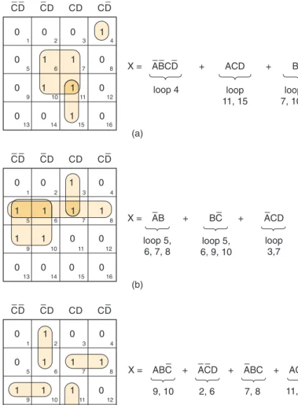
Note that each square in the top row is considered adjacent to a corresponding square in the bottom row. For example, the square in the top row is adjacent to the square in the bottom row, because they differ only in the A variable.
Looping
You might think that the top of the map is wrapped to touch the bottom of the map. Similarly, the squares in the leftmost column are adjacent to the corresponding squares in the rightmost column.
Looping Groups of Two (Pairs)
In the K map, the top and bottom rows of squares are considered adjacent. The two 1's in the bottom row are also adjacent because in the K map the leftmost column and the rightmost column of squares are considered adjacent.
Looping Groups of Four (Quads)
These two expressions can be concatenated (combined) to produce a resultant that eliminates the variable because it occurs in both uncomplemented and complemented form. The two can be created in a loop and the C-variable removed as it appears in its uncomplemented and complemented form to give the resultant.
Looping Groups of Eight (Octets)
The reader should check each of the other cases in Figure 4-13 to verify the expressions shown for X.
Complete Simplification Process
This square is looped because it contains two squares that were not previously looped. However, this quad is not a loop because all the 1's in the quad are included in other loops.
Filling a K Map from an Output Expression
Don’t-Care Conditions
The truth table is now complete, and we can transfer its information to the K-map in Figure 4-19(c). By changing four of these don't care squares to 1's, we can produce quadrilateral rings containing the original 1's [Figure 4-19(d)].
4-6 EXCLUSIVE-OR AND EXCLUSIVE-NOR CIRCUITS
There are other, more complex techniques that designers use to minimize logic circuits with more than four inputs. These techniques are particularly suitable for circuits with a large number of inputs where algebraic and K-mapping methods are not feasible.
Exclusive-OR
An XOR gate has only two inputs; there are no three-input or four-input XOR gates. The two inputs are combined so that a Shorthand way sometimes used to denote the XOR output expression is .
Exclusive-NOR
The IEEE/ANSI symbol adds the small triangle to the output of the XOR symbol. The output waveform is obtained by taking advantage of the fact that the XOR output goes HIGH only when the inputs are at different levels.
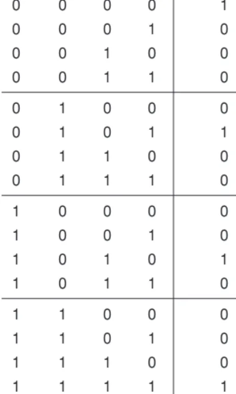
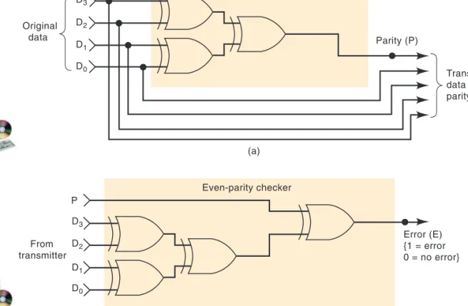
4-7 PARITY GENERATOR AND CHECKER
For each case, apply these levels to the inputs of the parity check and trace them down to the E output. Note that a 1 is only produced at E if an odd number of 1s appear in the parity check input.
4-8 ENABLE/DISABLE CIRCUITS
Conversely, when inverting gates (NAND, NOR) are enabled, the output will be the exact inverse of Asignal. EXAMPLE 4-21 Design a logic circuit that will allow a signal to pass to the output only when the Band Care control inputs are both HIGH; otherwise the output will remain LOW.
4-9 BASIC CHARACTERISTICS OF DIGITAL ICs
All the special ICs mentioned in Chapter 3 and this chapter are small port count SSI chips. In modern digital systems, medium-scale integration devices (MSI) and large-scale integration devices (LSI, VLSI, ULSI, GSI) perform most of the functions that once required multiple circuits full of SSI devices.
Bipolar and Unipolar Digital ICs
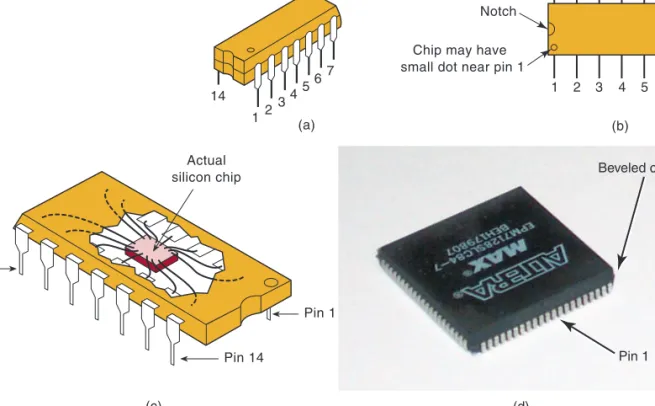
Note that pin 1 is not "on the corner" like the DIP, but rather in the middle of the top of the package. Due to the simplicity and compactness as well as some other superior properties of CMOS, the modern large-scale ICs are mainly manufactured using CMOS technology.
TTL Family
Teaching labs using SSI and MSI devices often use TTL because of its durability, although some also use CMOS.
CMOS Family
Power and Ground
Logic-Level Voltage Ranges
Unconnected (Floating) Inputs
While this is logically correct, it is not a recommended practice, especially in final circuit designs, because the floating TTL input is extremely sensitive to picking up noise signals that are likely to adversely affect device operation. Sometimes the output will oscillate due to the noise picked up by the floating input.
Logic-Circuit Connection Diagrams
For the circuit in Figure 4-32, the input signals are on the left. Note that in Figure 4-33 there are no pin codes or chip designations on the logic symbols.
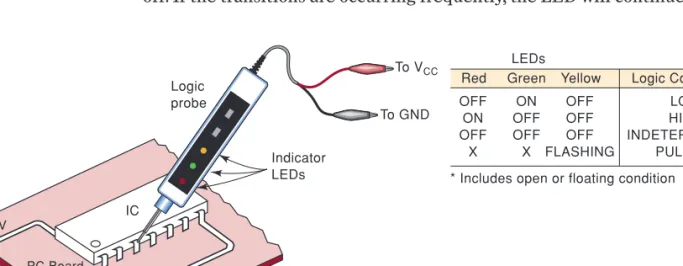
4-10 TROUBLESHOOTING DIGITAL SYSTEMS
However, we can help you develop the analytical skills that are the most essential part of effective problem solving. The logic level present at the probe tip is indicated by the status of the indicator LEDs in the probe.
4-11 INTERNAL DIGITAL IC FAULTS
Malfunction in Internal Circuitry
Input Internally Shorted to Ground or Supply
Output Internally Shorted to Ground or Supply
Open-Circuited Input or Output
At pin 6, the logic probe will show no LED lit for an undefined logic level because the NAND output level never reaches pin 6. This would be true if the open circuit had been external to the chip NAND.
Short Between Two Pins
Because the IC is TTL, this open circuit would produce the same effect as a logic HIGH on pin 1. If the IC had been CMOS, the internal open circuit on pin 1 could have produced an undefined output and overheating and possible destruction of the chip.
4-12 EXTERNAL FAULTS
Whenever you see a waveform like the Z1-2, Z1-4 signal in Figure 4-39 with three different levels, you should suspect that two output signals may be shorted together.
Open Signal Lines
Shorted Signal Lines
Faulty Power Supply
Output Loading
4-13 TROUBLESHOOTING CASE STUDY
All of these options, except the first, will short node X (and any IC pins connected to it) directly to VCC. When the pin that is internally shorted to VCC is disconnected, node X will no longer be shorted to VCC.
4-14 PROGRAMMABLE LOGIC DEVICES*
If the ICs are soldered to a circuit board, you'll need to cut the trace connected to the pin and fix the cut trace when you're done. You will have the opportunity to start developing your own troubleshooting skills by working on many problems at the end of the chapter that have been designated with a Tfor Troubleshooter.
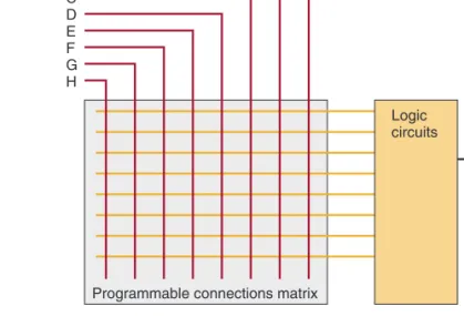
PLD Hardware
Input signals are connected to the columns of the matrix, and the outputs are connected to the rows of the matrix. By deciding which junctions are connected and which are not, we can "program" the way the inputs are connected to the outputs of the array.
Programming a PLD
Note that in this simple matrix we can produce any logical product combination of variables A, B at any AND gate outputs. A matrix or programmable array like the one shown in the figure can also be used to connect the AND outputs to the OR gates.